EP2602927A2 - Convertisseur modulair de plusieurs niveaux avec protection contre des fautes CC - Google Patents
Convertisseur modulair de plusieurs niveaux avec protection contre des fautes CC Download PDFInfo
- Publication number
- EP2602927A2 EP2602927A2 EP12008135.1A EP12008135A EP2602927A2 EP 2602927 A2 EP2602927 A2 EP 2602927A2 EP 12008135 A EP12008135 A EP 12008135A EP 2602927 A2 EP2602927 A2 EP 2602927A2
- Authority
- EP
- European Patent Office
- Prior art keywords
- type unit
- command value
- voltage
- unit converter
- voltage command
- Prior art date
- Legal status (The legal status is an assumption and is not a legal conclusion. Google has not performed a legal analysis and makes no representation as to the accuracy of the status listed.)
- Granted
Links
Images






Classifications
-
- H—ELECTRICITY
- H02—GENERATION; CONVERSION OR DISTRIBUTION OF ELECTRIC POWER
- H02M—APPARATUS FOR CONVERSION BETWEEN AC AND AC, BETWEEN AC AND DC, OR BETWEEN DC AND DC, AND FOR USE WITH MAINS OR SIMILAR POWER SUPPLY SYSTEMS; CONVERSION OF DC OR AC INPUT POWER INTO SURGE OUTPUT POWER; CONTROL OR REGULATION THEREOF
- H02M1/00—Details of apparatus for conversion
- H02M1/32—Means for protecting converters other than automatic disconnection
-
- H—ELECTRICITY
- H02—GENERATION; CONVERSION OR DISTRIBUTION OF ELECTRIC POWER
- H02M—APPARATUS FOR CONVERSION BETWEEN AC AND AC, BETWEEN AC AND DC, OR BETWEEN DC AND DC, AND FOR USE WITH MAINS OR SIMILAR POWER SUPPLY SYSTEMS; CONVERSION OF DC OR AC INPUT POWER INTO SURGE OUTPUT POWER; CONTROL OR REGULATION THEREOF
- H02M7/00—Conversion of AC power input into DC power output; Conversion of DC power input into AC power output
- H02M7/02—Conversion of AC power input into DC power output without possibility of reversal
- H02M7/04—Conversion of AC power input into DC power output without possibility of reversal by static converters
- H02M7/06—Conversion of AC power input into DC power output without possibility of reversal by static converters using discharge tubes without control electrode or semiconductor devices without control electrode
- H02M7/10—Conversion of AC power input into DC power output without possibility of reversal by static converters using discharge tubes without control electrode or semiconductor devices without control electrode arranged for operation in series, e.g. for multiplication of voltage
-
- H—ELECTRICITY
- H02—GENERATION; CONVERSION OR DISTRIBUTION OF ELECTRIC POWER
- H02M—APPARATUS FOR CONVERSION BETWEEN AC AND AC, BETWEEN AC AND DC, OR BETWEEN DC AND DC, AND FOR USE WITH MAINS OR SIMILAR POWER SUPPLY SYSTEMS; CONVERSION OF DC OR AC INPUT POWER INTO SURGE OUTPUT POWER; CONTROL OR REGULATION THEREOF
- H02M7/00—Conversion of AC power input into DC power output; Conversion of DC power input into AC power output
- H02M7/42—Conversion of DC power input into AC power output without possibility of reversal
- H02M7/44—Conversion of DC power input into AC power output without possibility of reversal by static converters
- H02M7/48—Conversion of DC power input into AC power output without possibility of reversal by static converters using discharge tubes with control electrode or semiconductor devices with control electrode
- H02M7/483—Converters with outputs that each can have more than two voltages levels
-
- H—ELECTRICITY
- H02—GENERATION; CONVERSION OR DISTRIBUTION OF ELECTRIC POWER
- H02M—APPARATUS FOR CONVERSION BETWEEN AC AND AC, BETWEEN AC AND DC, OR BETWEEN DC AND DC, AND FOR USE WITH MAINS OR SIMILAR POWER SUPPLY SYSTEMS; CONVERSION OF DC OR AC INPUT POWER INTO SURGE OUTPUT POWER; CONTROL OR REGULATION THEREOF
- H02M7/00—Conversion of AC power input into DC power output; Conversion of DC power input into AC power output
- H02M7/42—Conversion of DC power input into AC power output without possibility of reversal
- H02M7/44—Conversion of DC power input into AC power output without possibility of reversal by static converters
- H02M7/48—Conversion of DC power input into AC power output without possibility of reversal by static converters using discharge tubes with control electrode or semiconductor devices with control electrode
- H02M7/483—Converters with outputs that each can have more than two voltages levels
- H02M7/4835—Converters with outputs that each can have more than two voltages levels comprising two or more cells, each including a switchable capacitor, the capacitors having a nominal charge voltage which corresponds to a given fraction of the input voltage, and the capacitors being selectively connected in series to determine the instantaneous output voltage
-
- H—ELECTRICITY
- H02—GENERATION; CONVERSION OR DISTRIBUTION OF ELECTRIC POWER
- H02M—APPARATUS FOR CONVERSION BETWEEN AC AND AC, BETWEEN AC AND DC, OR BETWEEN DC AND DC, AND FOR USE WITH MAINS OR SIMILAR POWER SUPPLY SYSTEMS; CONVERSION OF DC OR AC INPUT POWER INTO SURGE OUTPUT POWER; CONTROL OR REGULATION THEREOF
- H02M1/00—Details of apparatus for conversion
- H02M1/0003—Details of control, feedback or regulation circuits
-
- H—ELECTRICITY
- H02—GENERATION; CONVERSION OR DISTRIBUTION OF ELECTRIC POWER
- H02M—APPARATUS FOR CONVERSION BETWEEN AC AND AC, BETWEEN AC AND DC, OR BETWEEN DC AND DC, AND FOR USE WITH MAINS OR SIMILAR POWER SUPPLY SYSTEMS; CONVERSION OF DC OR AC INPUT POWER INTO SURGE OUTPUT POWER; CONTROL OR REGULATION THEREOF
- H02M1/00—Details of apparatus for conversion
- H02M1/0064—Magnetic structures combining different functions, e.g. storage, filtering or transformation
-
- H—ELECTRICITY
- H02—GENERATION; CONVERSION OR DISTRIBUTION OF ELECTRIC POWER
- H02M—APPARATUS FOR CONVERSION BETWEEN AC AND AC, BETWEEN AC AND DC, OR BETWEEN DC AND DC, AND FOR USE WITH MAINS OR SIMILAR POWER SUPPLY SYSTEMS; CONVERSION OF DC OR AC INPUT POWER INTO SURGE OUTPUT POWER; CONTROL OR REGULATION THEREOF
- H02M1/00—Details of apparatus for conversion
- H02M1/0095—Hybrid converter topologies, e.g. NPC mixed with flying capacitor, thyristor converter mixed with MMC or charge pump mixed with buck
Definitions
- the present invention relates to a power conversion device, and particularly to a power conversion device formed using an arm where a plurality of unit converters are connected in series.
- MMCC modular multilevel cascade converter
- an MMCC-DSBC Double-Star Bridge Cell
- VSC-HVDC self-excited DC power transmission system
- an AC-DC converter has an AC terminal for linking to an AC system and a DC terminal for linking to a DC system.
- a voltage which is output to the AC system by the AC-DC converter is referred to as an AC output voltage
- a voltage which is output to the DC system by the AC-DC converter is referred to as a DC output voltage.
- a DC fault such as a DC ground fault or short-circuit caused by lightning, or the like, may occur.
- the MMCC-DSBC can control the switching timing of each switching element in the unit converter such that a DC output voltage becomes zero or a negative voltage, thereby suppressing a fault current from flowing into a DC fault point.
- the MMCC-DSCC can generate an AC output voltage which resists against an AC system voltage, and it is possible to suppress a fault current from flowing into the DC fault point from an AC system. Therefore, it is possible to rapidly resume power transmission after removing the DC fault without tripping the circuit breaker on the AC system side.
- an MMCC-DSCC which uses a bidirectionalbidirectionalchopper circuit as a unit converter and is formed from an arm where a plurality of unit converters are connected in series, it is necessary to trip the circuit breaker on the AC system side when a DC fault occurs, and thus it takes time to resume power transmission after removing the DC fault.
- the number of switching elements which allow current to flow at any one time is also substantially twice that of the MMCC-DSCC, and thus there is a problem in that there is substantially twice the amount of loss.
- a power conversion device includes at least two legs connected in parallel, each of which includes at least two unit converters having a power supply or an energy storage element, connected in series, wherein at least one of the legs is formed using at least two kinds of unit converters including a first type unit converter capable of outputting a unipolar voltage and a second type unit converter capable of outputting a bipolar voltage.
- each arm is constituted by two kinds of unit converters including a full bridge type unit converter and a bidirectional chopper.type unit converter.
- the power conversion device 102 is connected to an AC system 101 via a transformer 103.
- the AC system 101 side of the transformer 103 is set as a primary side which is referred to as an R point, an S point, and a T point
- a secondary side of the transformer 103 is referred to as an R' point, an S' point, and a T' point.
- the power conversion device 102 has DC terminals P point and N point, and a DC device 117 is connected between the P point and the N point.
- the DC device 117 is shown as a representative of a DC power supply, a DC load, or a power conversion device.
- a power conversion device with the same configuration as the power conversion device 102 may be connected as the DC device 117.
- the power conversion device 102 and the DC device 117 form a DC power transmission system.
- the power conversion device 102 includes a controller 112, and the controller 112 has a function of receiving a signal DCF from an external device via an external signal line 116.
- a DC fault 118 is a path which is short-circuited between the P point and the N point when a DC fault described later occurs.
- the power conversion device 102 includes the transformer 103, an R phase leg 104R, an S phase leg 104S, a T phase leg 104T, voltage sensors 110 and 115, current sensors 111, the controller 112, gate signal lines 113, and capacitor voltage detection lines 114.
- the R phase leg 104R is a circuit where an RP arm 105RP, a first reactor 107RP, a second reactor 107RN, and an RN arm 105RN are connected in series.
- a connection point between the reactor 107RP and the reactor 107RN is connected to the R' point of the transformer 103, a terminal on an opposite side to a terminal connected to the reactor 107RP of the RP arm 105RP is connected to the P point, and a terminal on an opposite side to a terminal connected to the reactor 107RN of the RN arm 105RN is connected to the N point.
- the S phase leg 104S is a circuit where an SP arm 105SP, a reactor (first reactor) 107SP, a reactor (second reactor) 107SN, and an SN arm 105SN are connected in series.
- a connection point of the reactor 107SP and the reactor 107SN is connected to the S' point of the transformer 103, a terminal on an opposite side to a terminal connected to the reactor 107SP of the SP arm 105SP is connected to the P point, and a terminal on an opposite side to a terminal connected to the reactor 107SN of the SN arm 105SN is connected to the N point.
- the T phase leg 104T is a circuit where a TP arm 105TP, a reactor (first reactor) 107TP, a reactor (second reactor) 107TN, and a TN arm 105TN are connected in series.
- a connection point of the reactor 107TP and the reactor 107TN is connected to the T' point of the transformer 103, a terminal on an opposite side to a terminal connected to the reactor 107TP of the TP arm 105TP is connected to the P point, and a terminal on an opposite side to a terminal connected to the reactor 107TN of the TN arm 105TN is connected to the N point.
- the RP arm 105RP is formed by serially connecting a bidirectional chopper group 106RPc which includes M bidirectional chopper type unit converters 108 connected in series to a full bridge group 106RPf which includes N full bridge type unit converters 109 connected in series.
- An output voltage of the bidirectional chopper group 106RPc is indicated by VRPc
- an output voltage of the full bridge group 106RPf is indicated by VRPf.
- the RN arm 105RN is formed by serially connecting a full bridge group 106RNf which includes N full bridge type unit converters 109 connected in series to a bidirectional chopper group 106RNc which includes M bidirectional chopper type unit converters 108 connected in series.
- An output voltage of the full bridge group 106RNf is indicated by VRNf
- an output voltage of the bidirectional chopper group 106RNc is indicated by VRNc.
- the SP arm 105SP is formed by serially connecting a bidirectional chopper group 106SPc which includes M bidirectional chopper type unit converters 108 connected in series to a full bridge group 106SPf which includes N full bridge type unit converters 109 connected in series.
- An output voltage of the bidirectional chopper group 106SPc is indicated by VSPc
- an output voltage of the full bridge group 106SPf is indicated by VSPf.
- the SN arm 105SN is formed by serially connecting a full bridge group 106SNf which includes N full bridge type unit converters 109 connected in series to a bidirectional chopper group 106SNc which includes M bidirectional chopper type unit converters 108 connected in series.
- An output voltage of the full bridge group 106SNf is indicated by VSNf
- an output voltage of the bidirectional chopper group 106SNc is indicated by VSNc.
- the TP arm 105TP is formed by serially connecting a bidirectional chopper group 106TPc which includes M bidirectional chopper type unit converters 108 connected in series to a full bridge group 106TPf which includes N full bridge type unit converters 109 connected in series.
- An output voltage of the bidirectional chopper group 106TPc is indicated by VTPc
- an output voltage of the full bridge group 106TPf is indicated by VTPf.
- the TN arm 105TN is formed by serially connecting a full bridge group 106TNf which includes N full bridge type unit converters 109 connected in series to a bidirectional chopper group 106TNc which includes M bidirectional chopper type unit converters 108 connected in series.
- An output voltage of the full bridge group 106TNf is indicated by VTNf
- an output voltage of the bidirectional chopper group 106TNc is indicated by VTNc.
- the respective arms 105RP, 105SP, 105TP, 105RN, 105SN and 105TN include the current sensors 111 which detect currents IRP, ISP, ITP, IRN, ISN and ITN flowing through the arms, and transmit detection results to the controller 112.
- a main circuit of the bidirectional chopper type unit converter 108 has a configuration in which a circuit where a parallel circuit of a switching element (high side switching element) 201H and a free wheel diode (high side free wheel diode) 202H and a parallel circuit of a switching element (low side switching element) 201L and a free wheel diode (low side free wheel diode) 202L are connected in series and a capacitor 203 are connected in parallel.
- FIG. 2 although the symbol for IGBT is used in the switching elements 201H and 201L, MOSFET, GCT, GTO, and other self-commutated elements may be used as the switching elements 201H and 201L.
- the bidirectional chopper type unit converter 108 includes a voltage sensor 204 which detects a capacitor voltage VCjk and is connected to the controller 112 via the capacitor voltage detection line 114.
- the bidirectional chopper type unit converter 108 includes a gate driver 205 which applies a gate voltage between the gate and the emitter of each of the switching elements 201H and 201L on the basis of gate signals GHjk and GLjk transmitted from the controller 112 via the gate signal line 113.
- the output voltage Vjk can be controlled so as to be substantially the same as zero regardless of a current Ij.
- the bidirectional chopper type unit converter 108 is a unit converter which can output a zero voltage or a unipolar voltage such as VCjk.
- a main circuit of the full bridge type unit converter 109 has a configuration in which a circuit where a parallel circuit of a switching element (X phase high side switching element) 201XH and a free wheel diode (X phase high side free wheel diode) 202XH and a parallel circuit of a switching element (X phase low side switching element) 201XL and a free wheel diode (X phase low side free wheel diode) 202XL are connected in series, a circuit where a parallel circuit of a switching element (Y phase high side switching element) 201YH and a free wheel diode (Y phase high side free wheel diode) 202YH and a parallel circuit of a switching element (Y phase low side switching element) 201YL and a free wheel diode (Y phase low side free wheel diode) 202YL are connected in series, and a capacitor 301 are connected in parallel.
- a serial connection point between the parallel circuit of the switching element (X phase high side switching element) 201XH and the free wheel diode (X phase high side free wheel diode) 202XH and the parallel circuit of the switching element (X phase low side switching element) 201XL and the free wheel diode (X phase low side free wheel diode) 202XL is referred to as an X point.
- a serial connection point between the parallel circuit of a switching element (Y phase high side switching element) 201YH and the free wheel diode (Y phase high side free wheel diode) 202YH and the parallel circuit of the switching element (Y phase low side switching element) 201YL and the free wheel diode (Y phase low side free wheel diode) 202YL is referred to as a Y point.
- a potential Vjk of the X point with respect to the Y point is referred to as an output voltage of the full bridge type unit converter 109.
- the full bridge type unit converter 109 includes a gate driver 302 which applies a gate voltage between the gate and the emitter of each of the switching elements 201XH, 201XL, 201YH and 201YL on the basis of gate signals GXHjk, GXLjk, GYHjk and GYLjk transmitted from the controller 112 via the gate signal line 113.
- the output voltage Vjk can be controlled so as to be substantially the same as zero regardless of a current Ij.
- the output voltage Vjk can be controlled so as to be substantially the same as the capacitor voltage VCjk regardless of a current Ij.
- the output voltage Vjk can be controlled so as to be substantially the same as a negative polarity voltage -VCjk of the capacitor voltage VCjk regardless of a current Ij.
- the output voltage Vjk can be controlled so as to be substantially the same as zero regardless of a current Ij.
- the full bridge type unit converter 109 is a unit converter which can output bipolar voltages such as VCjk, 0, and -VCjk.
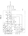
- Fig. 4 shows an AC voltage command value generation unit 412 which generates an AC voltage command value given to the power conversion device 102 and a DC voltage command value generation unit 413 which generates a DC voltage command value given thereto.
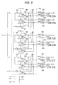
- Fig. 5 shows a command value distribution unit 504 which distributes a DC voltage command value and an AC voltage command value obtained in Fig. 4 to the respective unit converters 108 and 109, and a DC fault detection unit 505 which detects a DC fault.
- the respective units shown in Fig. 4 have a capacitor voltage control function of controlling an average value of capacitor voltages of the overall unit converters 108 and 109 so as to be constant, a current control function of controlling a d-axis current Id and a q-axis current Iq flowing through the AC system (power system) 101, and a function of generating an AC voltage command value and a DC voltage command value for realizing the two control functions.
- a difference VC*-VC between a capacitor voltage average value VC and a capacitor voltage command value VC* is multiplied by a capacitor voltage control gain 403, and a d-axis current command value Id* is obtained by further adding a d-axis current feed forward Idff* thereto.
- Idff* indicates a d-axis current command value for controlling active power which is supplied from the AC system 101 to the DC device 117 via the power conversion device 102.
- the d axis and q axis are set such that, in a case where the d-axis current is positive, active power flows into the power conversion device 102 from the AC system 101, and in a case where the d-axis current is negative, active power flows out of the power conversion device 102 to the AC system 101.
- a difference IRP-IRN between a current IRP flowing through the RP arm 105RP and a current IRN flowing through the RN arm 105RN, detected using the current sensors 111, that is, a current IR flowing through the AC system 101 is calculated.
- a current sensor for detecting IR may be provided separately.
- a difference ISP-ISN between a current ISP flowing through the SP arm 105SP and a current ISN flowing through the SN arm 105SN, detected using the current sensors 111, that is, a current IS flowing through the AC system 101 is calculated.
- a current sensor for detecting IS may be provided separately.
- a difference ITP-ITN between a current ITP flowing through the TP arm 105TP and a current ITN flowing through the TN arm 105TN, detected using the current sensors 111, that is, a current IT flowing through the AC system 101 is calculated.
- a current sensor for detecting IT may be provided separately.
- a phase angle ⁇ used for the d-q transform is a phase angle which is detected by a phase detector 411 from voltages VGR, VGS and VGT of the AC system 101 and is synchronized with a phase of VGR.
- a d-axis voltage command value Vd* and a q-axis voltage command value Vq* given to the power conversion device 102 are calculated based on Expressions (1) and (2) such that the d-axis current detection value Id conforms to a d-axis current command value Id*, and the q-axis current detection value Iq conforms to a q-axis current command value Iq*.
- Vd * VGd + Gain ⁇ Id * - Id + R ⁇ Id + X ⁇ Iq
- Vq * VGq + Gain ⁇ Iq * - Iq - Iq - X ⁇ Id + R ⁇ Iq
- VGd and VGq in Expressions (1) and (2) respectively indicate an AC system d-axis voltage and an AC system q-axis voltage obtained by performing the ⁇ - ⁇ transform and the d-q transform for the voltages VGR, VGS and VGT of the AC system 101.
- R in Expressions (1) and (2) is set to a sum of coil resistance of the transformer 103 and 1/2 of coil resistance of the reactor 107
- X is set to a sum of leakage reactance of the transformer 103 and 1/2 of reactance of the reactor 107.
- the AC voltage command value generation unit 412 performs inverse d-q transform and inverse ⁇ - ⁇ transform for Vd* and Vq* obtained using Expressions (1) and (2), thereby calculating AC voltage command values VR*, VS* and VT*.
- the DC voltage command value generation unit 413 generates a DC voltage command value VDC*.
- the R phase AC voltage command value VR* and the DC voltage command value VDC* are distributed to an output voltage command value VRPc* of the bidirectional chopper group 106RPc, an output voltage command value VRPf* of the full bridge group 106RPf, an output voltage command value VRNc* of the bidirectional chopper group 106RNc, and an output voltage command value VRNf* of the full bridge group 106RNf.
- VRPc * - m / m + n ⁇ D 2 ⁇ VR * + m / m + n ⁇ D ⁇ VDC * / 2
- VRNf * - 1 - m / m + n ⁇ D 2 ⁇ VR * + n / m + n ⁇ D ⁇ VDC * / 2
- VRNc * m / m + n ⁇ D 2 ⁇ VR * + m / m + n ⁇ D ⁇ VDC * / 2
- VRNf * 1 - m / m + n ⁇ D 2 ⁇ VR * + n / m + n ⁇ D ⁇ VDC * / 2
- D indicates a DC fault detection signal which is output by the DC fault detection unit 505 described later, and the signal becomes 1 when a DC fault is not detected and becomes 0 when a DC fault is detected.
- the S phase AC voltage command value VS* and the DC voltage command value VDC* are distributed to an output voltage command value VSPc* of the bidirectional chopper group 106SPc, an output voltage command value VSPf* of the full bridge group 106SPf, an output voltage command value VSNc* of the bidirectional chopper group 106SNc, and an output voltage command value VSNf* of the full bridge group 106SNf.
- VSPc * - m / m + n ⁇ D 2 ⁇ VS * + m / m + n ⁇ D ⁇ VDC * / 2
- VSPf * - 1 - m / m + n ⁇ D 2 ⁇ VS * + n / m + n ⁇ D ⁇ VDC * / 2
- VSNc * m / m + n ⁇ D 2 ⁇ VS * + m / m + n ⁇ D ⁇ VDC * / 2
- VSNf * 1 - m / m + n ⁇ D 2 ⁇ VS * + n / m + n ⁇ D ⁇ VDC * / 2
- n, n, and D are the same numbers as described above.
- the T phase AC voltage command value VT* and the DC voltage command value VDC* are distributed to an output voltage command value VTPc* of the bidirectional chopper group 106TPc, an output voltage command value VTPf* of the full bridge group 106TPf, an output voltage command value VTNc* of the bidirectional chopper group 106TNc, and an output voltage command value VTNf* of the full bridge group 106TNf.
- VTPc * - m / m + n ⁇ D 2 ⁇ VT * + m / m + n ⁇ D ⁇ VDC * / 2
- VTPf * - 1 - m / m + n ⁇ D 2 ⁇ VT * + n / m + n ⁇ D ⁇ VDC * / 2
- VTNc * m / m + n ⁇ D 2 ⁇ VT * + m / m + n ⁇ D ⁇ VDC * / 2
- VTNf * 1 - m / m + n ⁇ D 2 ⁇ VT * + n / m + n ⁇ D ⁇ VDC * / 2
- n, n, and D are the same numbers as described above.
- the bidirectional chopper type unit converter 108 or the full bridge type unit converter 109 fails, the failed unit converter is short-circuited.
- a ratio of a sum of the maximum output voltages of the bidirectional chopper type unit converters 108 in the arm 105 including the failed unit converter and a sum of the maximum output voltages of the full bridge type unit converters 109, that is, m:n varies.
- the command value distribution unit 504 and a command value distribution unit 701 of Fig. 7 described later may have a function of performing control such that the power conversion device 102 is continuously operated, by varying m and n described in Expressions (3) to (14) so as to vary a distribution ratio of the voltage command values, with respect to the arm 105 including the failed unit converter.
- ⁇ m is a ratio of the maximum output voltage of a single bidirectional chopper type unit converter 108 and a total of the maximum output voltages of M bidirectional chopper type unit converters 108 including the failed unit converter in the arm including the failed bidirectional chopper type unit converter 108.
- ⁇ n is a ratio of the maximum output voltage of a single full bridge type unit converter 109 and a total of the maximum output voltages of N full bridge type unit converters 109 including the failed unit converter in the arm including the failed full bridge type unit converter 109.
- the DC fault detection unit receives the DC system voltage VDC, the DC system current IDC, and the external signal DCF.
- VDC is smaller than a value which is set in advance or sequentially
- IDC is greater than a value which is set in advance or sequentially, or a predefined signal is received as the external signal DCF
- D is a signal which becomes 1 when a DC fault is not detected and becomes 0 when a DC fault is detected.
- a value between 0 and 1 may be used.
- the DC fault detection unit 505 After a specific time has elapsed from the detection of the DC fault, or in a case where a predefined signal is received as the external signal DCF, the DC fault detection unit 505 returns the DC fault detection signal D to 1 from 0. At this time, the DC fault detection unit 505 varies D from 0 to 1 instantaneously or with a certain slope. In Fig. 6 described later, a description will be made assuming that D is varied from 0 to 1 with a certain slope.
- the DC fault detection signal D may be given to the above-described command value distribution unit 504.
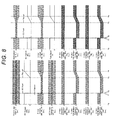
- Fig. 6 shows schematic waveforms of the AC system voltages VGR, VGS and VGT, the AC system currents IR, IS and IT, the DC system voltage VDC, the DC system current IDC, the currents IRP, ISP and ITP flowing through the arms 105RP, 105SP and 105TP, the currents IRN, ISN and ITN flowing through the arms 105RN, 105SN and 105TN, the AC voltage command values VR*, VS* and VT*, the DC fault detection signal D, voltage command values VRPc*, VSPc* and VTPc* given to the bidirectional chopper groups 106RPc, 106SPc and 106TPc, the output voltages VRPc, VSPc and VTPc of the bidirectional chopper groups 106RPc, 106SPc and 106TPc, the voltage command values VRPf*, VSPf* and VTPf* given to the full bridge groups 106RPf, 106SPf and 106TPf, the output voltages VRPf, V
- Fig. 6 exemplifies waveforms in a case where a ratio of the maximum output voltage of the bidirectional chopper type unit converter 108 and the maximum output voltage of the full bridge type unit converter 109 included in a single arm 105, that is, m:n is 1:1.
- the d-axis and q-axis current command values Id* and Iq* have finite values, and the power conversion device 102 receives active power P and reactive power Q from the AC system 101. In addition, power which is substantially the same as the received active power P is supplied to the DC device 117.
- the DC fault 118 occurs at the time point T1. If the DC fault 118 occurs at a location directly adjacent to the power conversion device 102, VDC becomes zero.
- the DC fault can be detected from the decrease in the DC system voltage VDC or the increase in the DC system current IDC.
- the DC fault detection unit 505 detects the DC fault, and varies the DC fault detection signal D from 1 to 0.
- the command value distribution unit 504 varies voltage command values given to the respective unit converters 108 and 109.
- the output voltage command values VRPc*, VSPc*, VTPc*, VRN*, VSN* and VTN* of the bidirectional chopper groups 106RPc, 106SPc, 106TPc, 106RNc, 106SNc and 106TNc are varied to zero
- DC components of the output voltage command values VRPf*, VSPf*, VTPf*, VRN*, VSN* and VTN* of the full bridge groups 106RPf, 106SPf, 106TPf, 106RNf, 106SNf and 106TNf are varied to zero
- AC components are varied doubly.
- the power conversion device 102 makes the d-axis current feed forward value Idff* for controlling active power received from the AC system 101 become zero at the time point T2.
- the currents IR, IS and IT flowing through the AC system substantially include only reactive current components corresponding to q-axis currents during the time period between the time points T2 and T3.
- the power conversion device 102 can maintain the function of supplying reactive power to the AC system 101 even in the circumstances where the DC fault occurs.
- Fig. 6 although a case where the q-axis current command value is controlled so as to be constant before and after the DC fault occurs, that is, constant reactive power is supplied has been exemplified, for example, when active power of the AC system 101 side rapidly varies due to a DC fault, there is a probability that power of the AC system 101 may fluctuate. In this case, it is possible to perform control so as to suppress power of the AC system 101 from fluctuating by using reactive power which is supplied to the AC system by the power conversion device 102.
- the DC system voltage VDC is zero, but DC components of output voltages of the respective bidirectional chopper type unit converters 108 and full bridge type unit converters 109 are also substantially zero, and thus it is possible to prevent the DC system current IDC from being overcurrent.
- the full bridge groups 106RPf, 106SPf, 106TPf, 106RNf, 106SNf and 106TNf output voltages resisting against the voltages VGR, VGS and VGT of the AC system 101, it is also possible to prevent a current from flowing into the DC fault 118 from the AC system 101.
- the overall unit converters are full bridge type unit converters, but, in the present invention, the bidirectional chopper type unit converter 108 and the full bridge type unit converter 109 are mixed, and thereby it is possible to reduce the number of the switching elements 201.
- the DC fault detection unit 505 gradually returns the DC fault detection signal D to 1 from 0 during the time period between the time points T3 and T4.
- the command value distribution unit 504 returns the output voltage command values VRPc*, VSPc*, VTPc*, VRNc*, VSNc* and VTNc* of the bidirectional chopper groups 106RPc, 106SPc, 106TPc, 106RNc, 106SNc and 106TNc, and the output voltage command values VRPf*, VSPf*, VTPf*, VRNf*, VSNf* and VTNf* of the full bridge groups 106RPf, 106SPf, 106TPf, 106RNf, 106SNf and 106TNf, to the waveforms before the DC fault occurs, that is, the same waveforms as those during the time period between the time points T0 and T1.
- the d-axis current feed forward Idff* is returned to the same waveform as that during the time period between the time point T0 and T1, and thus the currents IR, IS and IT flowing through the AC system are also returned to the same waveforms as those during the time period between the time points T0 and T1.
- the same effects can be achieved regardless of the serial connection order of the reactor 107TP, the bidirectional chopper group 106TPc, and the full bridge group 106TPf in the T phase leg 104T. Further, although not shown, the same effects can be achieved regardless of the serial connection order of the reactor 107TN, the bidirectional chopper group 106TNc, and the full bridge group 106TNf in the T phase leg 104T.
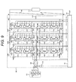
- FIGs. 1 and 9 exemplify the circuit diagrams where the bidirectional chopper type unit converters 108 are concentrated in the bidirectional chopper groups 106RPc, 106SPc, 106TPc, 106RNc, 106SNc and 106TNc, and the full bridge type unit converters 109 are concentrated in the full bridge groups 106RPf, 106SPf, 106TPf, 106RNf, 106SNf and 106TNf, for example, even if the bidirectional chopper type unit converters 108 and the full bridge type unit converters 109 are alternately connected in series, or, for example, even if the bidirectional chopper type unit converters 108 and the full bridge type unit converters 109 are randomly connected in series, the same effects can be achieved.
- each leg may be constituted by only one kind of unit converter.
- a ratio of a sum of the maximum output voltages of the bidirectional chopper type unit converters 108 and a sum of the maximum output voltages of the full bridge type unit converters 109 in the R phase leg 104R is indicated by mr:nr.
- a ratio of a sum of the maximum output voltages of the bidirectional chopper type unit converters 108 and a sum of the maximum output voltages of the full bridge type unit converters 109 in the S phase leg 104S is indicated by ms:ns.
- a ratio of a sum of the maximum output voltages of the bidirectional chopper type unit converters 108 and a sum of the maximum output voltages of the full bridge type unit converters 109 in the T phase leg 104T is indicated by mt:nt.
- the AC voltage command value generation unit 412, the DC voltage command value generation unit 413, and the DC fault detection unit 505 can be used.
- the command value distribution unit 504 methods different from that shown in Fig. 5 are used. Although not shown, an operation principle thereof will now be described.
- an operation of the power conversion device 102 according to a third embodiment is the same as that described with reference to Fig. 6 .
- VRPf * - nr - ns + nt / nr + ns + nt ⁇ VR * - VS * + nr + ns - nt / nr + ns + nt ⁇ VT * - VR *
- VSPf * - nr + ns - nt / nr + ns + nt ⁇ VS * - VT * + - nr + ns + nt / nr + ns + nt ⁇ VR * - VS *
- VTPf * - - nr + ns + nt / nr + ns + nt ⁇ VT * - VR * + nr + ns - ns + nt ⁇ VT * - VR * + nr + ns - nt / / nr + ns + nt ⁇ VR
- the second embodiment is characterized in that the command value distribution unit 701 shown in Fig. 7 is employed instead of the command value distribution unit 504 according to the first embodiment.
- the R phase AC voltage command value VR* and the DC voltage command value VDC* are distributed to an output voltage command value VRPc* of the bidirectional chopper group 106RPc, an output voltage command value VRPf* of the full bridge group 106RPf, an output voltage command value VRNc* of the bidirectional chopper group 106RNc, and an output voltage command value VRNf* of the full bridge group 106RNf.
- VRPc * - m / m + n ⁇ VR * + m / m + n ⁇ VDC * / 2
- VRPf * - n / m + n ⁇ VR * + D - 1 ⁇ m + Dn / m + n ⁇ VDC * / 2
- VRNc * m / m + n ⁇ VR * + m / m + n ⁇ VDC * / 2
- VRNf * n / m + n ⁇ VR * + D - 1 ⁇ m + Dn / m + n ⁇ VDC * / 2
- D indicates a DC fault detection signal which is output by the DC fault detection unit 505 described later, and the signal becomes 1 when a DC fault is not detected and becomes 0 when a DC fault is detected.
- the second embodiment is characterized in that the DC fault detection signal D is not included in the voltage command values VRPc* and VRNc* which are given to the bidirectional chopper groups 106RPc and 106RNc unlike in the first embodiment.
- the S phase AC voltage command value VS* and the DC voltage command value VDC* are distributed to an output voltage command value VSPc* of the bidirectional chopper group 106SPc, an output voltage command value VSPf* of the full bridge group 106SPf, an output voltage command value VSNc* of the bidirectional chopper group 106SNc, and an output voltage command value VSNf* of the full bridge group 106SNf.
- VSPc * - m / m + n ⁇ VS * + m / m + n ⁇ VDC * / 2
- VSPf * - n / m + n ⁇ VS * + D - 1 ⁇ m + Dn / m + n ⁇ VDC * / 2
- VSNc * m / m + n ⁇ VS * + m / m + n ⁇ VDC * / 2
- VSNf * n / m + n ⁇ VS * + D - 1 ⁇ m + Dn / m + n ⁇ VDC * / 2
- n, n, and D are the same numbers as described above.
- the T phase AC voltage command value VT* and the DC voltage command value VDC* are distributed to an output voltage command value VTPc* of the bidirectional chopper group 106TPc, an output voltage command value VTPf* of the full bridge group 106TPf, an output voltage command value VTNc* of the bidirectional chopper group 106TNc, and an output voltage command value VTNf* of the full bridge group 106TNf.
- VTPc * - m / m + n ⁇ VT * + m ⁇ m + n ⁇ VDC * / 2
- VTPf * - n / m + n ⁇ VT * + D - 1 ⁇ m + Dn / m + n ⁇ VDC * / 2
- VTNc * m / m + n ⁇ VT * + m ⁇ m + n ⁇ VDC * / 2
- VTNf * n / m + n ⁇ VT * + D - 1 ⁇ m + Dn / m + n ⁇ VDC * / 2
- n, n, and D are the same numbers as described above.
- Fig. 8 shows schematic waveforms of the AC system voltages VGR, VGS and VGT, the AC system currents IR, IS and IT, the DC system voltage VDC, the DC system current IDC, the currents IRP, ISP and ITP flowing through the arms 105RP, 105SP and 105TP, the currents IRN, ISN and ITN flowing through the arms 105RN, 105SN and 105TN, the AC voltage command values VR*, VS* and VT*, the DC fault detection signal D, voltage command values VRPc*, VSPc* and VTPc* given to the bidirectional chopper groups 106RPc, 106SPc and 106TPc, the output voltages VRPc, VSPc and VTPc of the bidirectional chopper groups 106RPc, 106SPc and 106TPc, the voltage command values VRPf*, VSPf* and VTPf* given to the full bridge groups 106RPf, 106SPf and 106TPf, the output voltages VRPf, V
- Fig. 8 exemplifies waveforms in a case where a ratio of the maximum output voltage of the bidirectional chopper type unit converter 108 and the maximum output voltage of the full bridge type unit converter 109 included in a single arm 105, that is, m:n is 1:1.
- the d-axis and q-axis current command values Id* and Iq* have finite values, and the power conversion device 102 receives active power P and reactive power Q from the AC system 101. In addition, power which is substantially the same as the received active power P is supplied to the DC device 117.
- the DC fault 118 occurs at the time point T1. If the DC fault 118 occurs at a location directly adjacent to the power conversion device 102, VDC becomes zero.
- VDC becomes zero
- the overall DC voltages generated by the bidirectional chopper type unit converters 108 and the full bridge type unit converters 109 of the respective legs 104R, 104S and 104T are applied to the reactors 107RP, 107RN, 107SP, 107SN, 107TP and 107TN. For this reason, the DC system current IDC increases.
- the DC fault can be detected from the decrease in the DC system voltage VDC or the increase in the DC system current IDC.
- the DC fault detection unit 505 detects the DC fault, and varies the DC fault detection signal D from 1 to 0.
- the command value distribution unit 701 varies voltage command values given to the full bridge type unit converters 109.
- DC components of the output voltage command values VRPf*, VSPf*, VTPf*, VRN*, VSN* and VTN* of the full bridge groups 106RPf, 106SPf, 106TPf, 106RNf, 106SNf and 106TNf are varied such that DC components of the output voltage command values VRPc*, VSPc*, VTPc*, VRN* VSN* and VTN* of the bidirectional chopper groups 106RPc, 106SPc, 106TPc, 106RNc, 106SNc and 106TNc and DC components of the output voltage command values VRPf*, VSPf*, VTPf*, VRN* VSN* and VTN* of the bidirectional chopper groups 106RPc, 106SPc, 106TPc, 106RNc, 106SNc and 106TNc and DC components of the output voltage command values VRPf*, VSPf*, VTPf*, VRN*, VSN* and VTN* of the full bridge groups
- the power conversion device 102 makes the d-axis current feed forward value Idff* for controlling active power received from the AC system 101 become zero at the time point T2.
- the currents IR, IS and IT flowing through the AC system substantially include only reactive current components corresponding to q-axis currents during the time period between the time points T2 and T3.
- the DC system voltage VDC is zero, but DC components of output voltages of the bidirectional chopper type unit converters 108 and DC components of output voltages of the full bridge type unit converters 109 are substantially canceled out, and thus it is possible to prevent the DC system current IDC from being overcurrent.
- the overall unit converters are full bridge type unit converters, but, in the present invention, the bidirectional chopper type unit converter 108 and the full bridge type unit converter 109 are mixed, and thereby it is possible to reduce the number of the switching elements 201.
- the DC fault detection unit 505 gradually returns the DC fault detection signal D to 1 from 0 during the time period of the time points T3 and T4.
- the command value distribution unit 701 returns the output voltage command values VRPf*, VSPf*, VTPf*, VRNf*, VSNf* and VTNf* of the full bridge groups 106RPf, 106SPf, 106TPf, 106RNf, 106SNf and 106TNf, to the waveforms before the DC fault occurs, that is, the same waveforms as those during the time period between the time points T0 and T1.
- the d-axis current feed forward Idff* is returned to the same waveform as that during the time period between the time point T0 and T1, and thus the currents IR, IS and IT flowing through the AC system are also returned to the same waveforms as those during the time period between the time points T0 and T1.
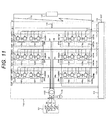
- a power conversion device 1101 of Fig. 11 described in the present invention is characterized in that a double Y-connection transformer 1102 is used instead of the transformer 103 and the reactors 107RP, 107SP, 107TP, 107RN, 107SN and 107TN.
- the double Y-connection transformer 1102 has a P side secondary winding 1203P and an N side secondary winding 1203N described later.
- Fig. 12 shows a winding structure of the double Y-connection transformer 1102, and details thereof will be described later.
- terminals of the P side secondary winding 1203P are referred to as an RP point, an SP point, and a TP point, which are respectively connected to the RP arm 105RP, the SP arm 105SP, and the TP arm 105TP.
- terminals of the N side secondary winding 1203N are referred to as an RN point, an SN point, and a TN point, which are respectively connected to the RN arm 105RN, the SP arm 105SN, and the TN arm 105TN.
- the double Y-connection transformer includes an iron core 1201 which has at least three legs 1201R, 1201S and 1201T, and, an R phase primary winding 1204R, an S phase primary winding 1204S, and a T phase primary winding 1204T are wound thereon, respectively.
- the three primary windings 1204R, 1204S and 1204T form a start-connection but may form a delta-connection.
- the P side secondary winding 1203P includes an R phase P side secondary winding 1205RP, an S phase P side secondary winding 1205SP, and a T phase P side secondary winding 1205TP which are respectively wound on the legs 1201R, 1201S and 1201T so as to form a star-connection.
- the N side secondary winding 1203N includes an R phase N side secondary winding 1205RN, an S phase N side secondary winding 1205SN, and a T phase N side secondary winding 1205TN which are respectively wound on the legs 1201R, 1201S and 1201T so as to form a star-connection.
- the R phase P side secondary winding 1205RP and the R phase N side secondary winding 1205RN wound on the leg 1201R are magnetically coupled to each other such that the magnetomotive forces thereof have opposite polarities.
- the S phase P side secondary winding 1205SP and the S phase N side secondary winding 1205SN wound on the leg 1201S are magnetically coupled to each other such that the magnetomotive forces thereof have opposite polarities.
- the T phase P side secondary winding 1205TP and the T phase N side secondary winding 1205TN wound on the leg 1201T are magnetically coupled to each other such that the magnetomotive forces thereof have opposite polarities.
- a point for forming the star-connection of the P side secondary winding 1203P is electrically connected to a point for forming the star-connection of the N side secondary winding 1203N.
- the AC voltage command value generation unit 412, the DC voltage command value generation unit 413, and the command value distribution units 504 and 701 described in the first and second embodiments can be used, and, the power conversion device 1101 can be controlled using the same control method as the control method described in the first and second embodiments.
Landscapes
- Engineering & Computer Science (AREA)
- Power Engineering (AREA)
- Inverter Devices (AREA)
- Rectifiers (AREA)
- Dc-Dc Converters (AREA)
Applications Claiming Priority (1)
| Application Number | Priority Date | Filing Date | Title |
|---|---|---|---|
| JP2011267453A JP5894777B2 (ja) | 2011-12-07 | 2011-12-07 | 電力変換装置 |
Publications (3)
| Publication Number | Publication Date |
|---|---|
| EP2602927A2 true EP2602927A2 (fr) | 2013-06-12 |
| EP2602927A3 EP2602927A3 (fr) | 2014-08-06 |
| EP2602927B1 EP2602927B1 (fr) | 2018-02-21 |
Family
ID=47357852
Family Applications (1)
| Application Number | Title | Priority Date | Filing Date |
|---|---|---|---|
| EP12008135.1A Active EP2602927B1 (fr) | 2011-12-07 | 2012-12-05 | Convertisseur modulair de plusieurs niveaux avec protection contre des fautes CC |
Country Status (3)
| Country | Link |
|---|---|
| US (1) | US9190930B2 (fr) |
| EP (1) | EP2602927B1 (fr) |
| JP (1) | JP5894777B2 (fr) |
Cited By (12)
| Publication number | Priority date | Publication date | Assignee | Title |
|---|---|---|---|---|
| CN103929088A (zh) * | 2014-04-18 | 2014-07-16 | 华北电力大学 | 一种模块化多电平换流器的平均值模型 |
| EP2830200A1 (fr) * | 2013-07-25 | 2015-01-28 | Alstom Technology Ltd | Convertisseur de puissance |
| EP2863534A1 (fr) * | 2013-10-16 | 2015-04-22 | Alstom Technology Ltd | Convertisseur de source de tension |
| EP2975749A1 (fr) * | 2014-07-15 | 2016-01-20 | General Electric Company | Convertisseur d'énergie à plusieurs niveaux |
| WO2016128162A1 (fr) * | 2015-02-09 | 2016-08-18 | Siemens Aktiengesellschaft | Système d'alimentation en courant de traction et procédé permettant de faire fonctionner ledit système |
| WO2016156416A1 (fr) * | 2015-03-30 | 2016-10-06 | General Electric Technology Gmbh | Commande de convertisseurs sources de tension |
| KR20180017888A (ko) * | 2016-08-11 | 2018-02-21 | 연세대학교 산학협력단 | 멀티레벨 컨버터 hvdc 시스템에서 dc 사고 감지 장치 및 방법 |
| EP3285388A4 (fr) * | 2015-04-13 | 2018-12-26 | Mitsubishi Electric Corporation | Dispositif de conversion de puissance électrique |
| CN109378788A (zh) * | 2018-11-08 | 2019-02-22 | 国网湖南省电力有限公司 | 新型svg型直流融冰装置 |
| CN111049407A (zh) * | 2020-01-03 | 2020-04-21 | 东南大学 | 具有断流能力的混联型模块化多电平变换器及其控制方法 |
| EP3751718A1 (fr) * | 2019-06-12 | 2020-12-16 | Siemens Aktiengesellschaft | Procédé de traitement de défauts dans une ligne de tension continue ainsi que dispositif convertisseur de courant permettant la mise en oeuvre dudit procédé |
| EP4322388A4 (fr) * | 2021-04-05 | 2024-05-15 | Mitsubishi Electric Corporation | Dispositif de conversion d'énergie |
Families Citing this family (44)
| Publication number | Priority date | Publication date | Assignee | Title |
|---|---|---|---|---|
| JP5894777B2 (ja) * | 2011-12-07 | 2016-03-30 | 株式会社日立製作所 | 電力変換装置 |
| WO2014033155A1 (fr) * | 2012-08-28 | 2014-03-06 | Abb Technology Ag | Commande de convertisseur modulaire en deux étages |
| US20150288287A1 (en) * | 2012-09-21 | 2015-10-08 | Aukland Uniservices Limited | Modular multi-level converters |
| EP2946464B1 (fr) * | 2013-01-21 | 2019-12-18 | ABB Schweiz AG | Convertisseur multiniveaux à cellules hybrides en pont complet |
| CN104300814B (zh) * | 2013-07-18 | 2017-02-15 | 南京南瑞继保电气有限公司 | 一种模块化多电平电压源换流器及其控制方法 |
| CN103633871B (zh) * | 2013-11-20 | 2016-10-05 | 华南理工大学 | 基于全桥与半桥模块的混合型多电平换流器及其控制方法 |
| CN103715930B (zh) * | 2013-11-25 | 2016-09-21 | 国家电网公司 | 一种提升柔性直流输电系统容量的方法 |
| CN103715935B (zh) * | 2013-11-27 | 2016-09-28 | 国家电网公司 | 一种基于模块化多电平电压源型换流器的损耗确定方法 |
| US9991713B2 (en) * | 2014-02-19 | 2018-06-05 | ABB Schweiz AB | Energy storage system comprising a modular multi-level converter |
| CN103792854B (zh) * | 2014-03-03 | 2016-11-23 | 上海科梁信息工程股份有限公司 | 基于模块化多电平换流器的柔性直流输电半实物仿真系统 |
| CN104052026B (zh) * | 2014-05-29 | 2016-05-25 | 华中科技大学 | 用于模块化多电平换流器的子模块拓扑及其应用 |
| JP6342233B2 (ja) * | 2014-06-25 | 2018-06-13 | 株式会社日立製作所 | 電力変換装置 |
| JP6288773B2 (ja) * | 2014-06-26 | 2018-03-07 | 東芝三菱電機産業システム株式会社 | 電力変換装置 |
| EP2988406A1 (fr) * | 2014-08-19 | 2016-02-24 | Alstom Technology Ltd | Améliorations apportées ou se rapportant aux commandes de convertisseurs |
| CN104362616B (zh) * | 2014-10-20 | 2017-02-01 | 许继电气股份有限公司 | 全桥子模块模块化多电平换流器直流短路故障穿越方法 |
| JP6261491B2 (ja) * | 2014-11-19 | 2018-01-17 | 三菱電機株式会社 | 電力変換装置 |
| JP6062132B1 (ja) * | 2015-04-13 | 2017-01-18 | 三菱電機株式会社 | 電力変換装置および電力システム |
| CN104767227B (zh) * | 2015-04-18 | 2018-11-06 | 东北电力大学 | 一种智能配电网变电装置母线潮流控制器 |
| DK3309949T3 (da) * | 2015-06-15 | 2020-03-23 | Toshiba Mitsubishi Elec Ind | Effektomformningsindretning |
| US10326355B2 (en) * | 2015-07-14 | 2019-06-18 | Mitsubishi Electric Corporation | Power conversion device |
| CN106487254B (zh) * | 2015-08-28 | 2019-07-09 | 国网智能电网研究院 | 一种基于相似判据的mmc换流阀动模系统参数设计方法 |
| KR101774978B1 (ko) * | 2015-12-31 | 2017-09-05 | 주식회사 효성 | Hvdc용 mmc의 리던던시 제어방법 |
| CN107346003B (zh) * | 2016-05-05 | 2020-09-08 | 南京南瑞继保电气有限公司 | 一种电压源换流器故障检测定位方法和系统 |
| FR3053854B1 (fr) * | 2016-07-05 | 2018-08-17 | Supergrid Institute | Module de controle de l'energie interne d'un convertisseur |
| EP3514941B1 (fr) | 2016-09-13 | 2020-12-09 | Mitsubishi Electric Corporation | Appareil de conversion de puissance et système électrique |
| DE102017202204A1 (de) * | 2017-02-13 | 2018-08-16 | Siemens Aktiengesellschaft | Umrichteranordnung |
| WO2018184669A1 (fr) * | 2017-04-05 | 2018-10-11 | Abb Schweiz Ag | Compensation de décalage de courant continu dans un convertisseur multiniveau modulaire |
| CN106953530B (zh) * | 2017-04-21 | 2018-11-20 | 上海交通大学 | 混合型mmc不对称双子模块和半桥子模块的配置方法 |
| FR3068842B1 (fr) * | 2017-07-07 | 2022-03-04 | Inst Supergrid | Convertisseur muni d'un module de gestion de l'energie en partie alternative |
| US11289996B2 (en) * | 2017-07-31 | 2022-03-29 | Siemens Energy Global GmbH & Co. KG | Converter assembly with an ability to disconnect a fault current and a method for disconnecting a fault current at a converter assembly of this type |
| EP3667893B1 (fr) * | 2017-08-09 | 2021-09-22 | Mitsubishi Electric Corporation | Dispositif de conversion de puissance |
| CN107728508B (zh) * | 2017-09-01 | 2019-11-01 | 中国南方电网有限责任公司电网技术研究中心 | 一种柔性直流系统的控制保护方法及其控制保护装置 |
| US11309787B2 (en) * | 2017-09-26 | 2022-04-19 | MitsubishiI Electric Corporation | Power conversion device |
| CN107994599B (zh) * | 2017-12-07 | 2020-10-16 | 南京南瑞继保电气有限公司 | 一种串联式电压源换流阀组的协调控制方法及装置 |
| WO2019215842A1 (fr) * | 2018-05-09 | 2019-11-14 | 株式会社東芝 | Dispositif de conversion de puissance |
| JP7051012B2 (ja) * | 2018-11-27 | 2022-04-08 | ヒタチ・エナジー・スウィツァーランド・アクチェンゲゼルシャフト | 位相リアクトルのないstatcom構成 |
| EP3734818B1 (fr) * | 2019-04-29 | 2022-06-29 | Siemens Energy Global GmbH & Co. KG | Procédé de traitement d'un défaut dans une conduite de tension continue ainsi que dispositif convertisseur de courant permettant la mise en oeuvre dudit procédé |
| JP7374734B2 (ja) * | 2019-11-26 | 2023-11-07 | 東芝インフラシステムズ株式会社 | 電力変換装置 |
| JP6768993B1 (ja) * | 2019-12-02 | 2020-10-14 | 三菱電機株式会社 | 電力変換装置 |
| EP4071996A4 (fr) * | 2019-12-03 | 2022-11-23 | Mitsubishi Electric Corporation | Dispositif de conversion de puissance |
| CN112016043B (zh) * | 2020-07-06 | 2023-09-19 | 北京交通大学 | 模块化多电平换流器的稳态故障电流的计算方法 |
| WO2023144911A1 (fr) * | 2022-01-26 | 2023-08-03 | 三菱電機株式会社 | Dispositif de conversion d'énergie et procédé de commande de dispositif de conversion d'énergie |
| CN117192322B (zh) * | 2023-10-27 | 2025-03-28 | 深圳市深鸿盛电子有限公司 | 碳化硅晶体管的电压检测分析方法及系统 |
| CN120034009A (zh) * | 2023-11-22 | 2025-05-23 | 上海交通大学 | 电力电子变压器 |
Family Cites Families (19)
| Publication number | Priority date | Publication date | Assignee | Title |
|---|---|---|---|---|
| EP1756926B1 (fr) | 2004-06-18 | 2007-11-07 | ABB Schweiz AG | Procede de traitement de defaut dans un circuit convertisseur pour la commutation de trois niveaux de tension |
| DE102005040543A1 (de) * | 2005-08-26 | 2007-03-01 | Siemens Ag | Stromrichterschaltung mit verteilten Energiespeichern |
| ES2693612T3 (es) * | 2007-03-13 | 2018-12-12 | Siemens Aktiengesellschaft | Procedimiento para la limitación de daños de un convertidor de corriente que presenta semiconductores de potencia en caso de un cortocircuito en el circuito intermedio de tensión continua |
| US8792261B2 (en) | 2009-03-30 | 2014-07-29 | Hitachi, Ltd. | Power conversion device |
| JP5268739B2 (ja) * | 2009-03-30 | 2013-08-21 | 株式会社日立製作所 | 電力変換装置 |
| CA2759818C (fr) * | 2009-05-07 | 2016-11-01 | Abb Technology Ag | Procede et agencement pour determiner la tension de condensateur d'une cellule de convertisseur de puissance a multiples cellules |
| JP4969614B2 (ja) * | 2009-07-21 | 2012-07-04 | 株式会社日立製作所 | 電力変換装置 |
| JP5449893B2 (ja) * | 2009-07-21 | 2014-03-19 | 株式会社日立製作所 | 電力変換装置 |
| JP4934703B2 (ja) * | 2009-07-21 | 2012-05-16 | 株式会社日立製作所 | 電力変換装置 |
| WO2011012174A1 (fr) * | 2009-07-31 | 2011-02-03 | Areva T&D Uk Limited | Convertisseur doté dune limitation active de courant de défaut |
| JP5176006B2 (ja) * | 2009-10-06 | 2013-04-03 | エー ビー ビー リサーチ リミテッド | 電圧形コンバータ |
| JP5592236B2 (ja) * | 2010-11-01 | 2014-09-17 | 株式会社日立製作所 | 電力変換装置 |
| US20130308235A1 (en) | 2011-02-01 | 2013-11-21 | Siemens Aktiengesellschaft | Method for eliminating a fault on a high-voltage dc line, system for transmitting an electric current via a high-voltage dc line, and converter |
| JP5894777B2 (ja) * | 2011-12-07 | 2016-03-30 | 株式会社日立製作所 | 電力変換装置 |
| DK2806552T3 (en) * | 2012-01-18 | 2017-01-09 | Toshiba Mitsubishi-Electric Ind Systems Corp | Energy converter layout |
| US9219426B2 (en) * | 2012-02-09 | 2015-12-22 | Hitachi, Ltd. | Switching element, power converter, direct current transmission system, current control device, method of controlling power converter, and method of controlling current in voltage source converter |
| JP5775033B2 (ja) * | 2012-07-11 | 2015-09-09 | 株式会社日立製作所 | 電圧型電力変換装置の制御装置及び制御方法 |
| JP5993675B2 (ja) * | 2012-09-14 | 2016-09-14 | 株式会社日立製作所 | 電力変換装置,電力変換システム及び電力変換装置の制御方法 |
| JP6018934B2 (ja) * | 2013-01-25 | 2016-11-02 | 株式会社日立製作所 | 電力変換装置 |
-
2011
- 2011-12-07 JP JP2011267453A patent/JP5894777B2/ja active Active
-
2012
- 2012-12-05 EP EP12008135.1A patent/EP2602927B1/fr active Active
- 2012-12-06 US US13/706,638 patent/US9190930B2/en active Active
Non-Patent Citations (2)
| Title |
|---|
| H. AKAGI: "Classification, terminology, and applications of the modular multilevel converter (MMCC", IEEE TRANS. POWER ELECTRON., vol. 26, no. 11, November 2011 (2011-11-01), pages 3119 - 3130 |
| R. S. WHITEHOUSE: "Technical Challenges of realizing multi-terminal networking with VSC", EPE, 2011 |
Cited By (26)
| Publication number | Priority date | Publication date | Assignee | Title |
|---|---|---|---|---|
| US10284103B2 (en) | 2013-07-25 | 2019-05-07 | General Electric Technology Gmbh | Power converter operable during a fault condition |
| EP2830200A1 (fr) * | 2013-07-25 | 2015-01-28 | Alstom Technology Ltd | Convertisseur de puissance |
| WO2015011249A1 (fr) * | 2013-07-25 | 2015-01-29 | Alstom Technology Ltd | Convertisseur de courant |
| US9853574B2 (en) | 2013-10-16 | 2017-12-26 | General Electric Technology Gmbh | Voltage source converter |
| EP2863534A1 (fr) * | 2013-10-16 | 2015-04-22 | Alstom Technology Ltd | Convertisseur de source de tension |
| WO2015055682A1 (fr) * | 2013-10-16 | 2015-04-23 | Alstom Technology Ltd | Convertisseur de source de tension |
| CN103929088A (zh) * | 2014-04-18 | 2014-07-16 | 华北电力大学 | 一种模块化多电平换流器的平均值模型 |
| CN103929088B (zh) * | 2014-04-18 | 2017-01-04 | 华北电力大学 | 一种模块化多电平换流器的平均值模型 |
| EP2975749A1 (fr) * | 2014-07-15 | 2016-01-20 | General Electric Company | Convertisseur d'énergie à plusieurs niveaux |
| CN105281355A (zh) * | 2014-07-15 | 2016-01-27 | 通用电气公司 | 多级功率转换器 |
| US9667167B2 (en) | 2014-07-15 | 2017-05-30 | General Electric Company | Systems and methods for power conversion with direct current fault ride-through capability |
| WO2016128162A1 (fr) * | 2015-02-09 | 2016-08-18 | Siemens Aktiengesellschaft | Système d'alimentation en courant de traction et procédé permettant de faire fonctionner ledit système |
| RU2669786C1 (ru) * | 2015-02-09 | 2018-10-16 | Сименс Акциенгезелльшафт | Устройство для тягового электроснабжения и способ эксплуатации устройства |
| CN107431428A (zh) * | 2015-03-30 | 2017-12-01 | 通用电器技术有限公司 | 电压源换流器的控制 |
| CN113872425A (zh) * | 2015-03-30 | 2021-12-31 | 通用电器技术有限公司 | 电压源换流器的控制 |
| WO2016156416A1 (fr) * | 2015-03-30 | 2016-10-06 | General Electric Technology Gmbh | Commande de convertisseurs sources de tension |
| US10763742B2 (en) | 2015-03-30 | 2020-09-01 | General Electric Technology Gmbh | Control of voltage source converters |
| EP3285388A4 (fr) * | 2015-04-13 | 2018-12-26 | Mitsubishi Electric Corporation | Dispositif de conversion de puissance électrique |
| KR101882908B1 (ko) | 2016-08-11 | 2018-07-27 | 연세대학교 산학협력단 | 멀티레벨 컨버터 hvdc 시스템에서 dc 사고 감지 장치 및 방법 |
| KR20180017888A (ko) * | 2016-08-11 | 2018-02-21 | 연세대학교 산학협력단 | 멀티레벨 컨버터 hvdc 시스템에서 dc 사고 감지 장치 및 방법 |
| CN109378788A (zh) * | 2018-11-08 | 2019-02-22 | 国网湖南省电力有限公司 | 新型svg型直流融冰装置 |
| EP3751718A1 (fr) * | 2019-06-12 | 2020-12-16 | Siemens Aktiengesellschaft | Procédé de traitement de défauts dans une ligne de tension continue ainsi que dispositif convertisseur de courant permettant la mise en oeuvre dudit procédé |
| CN111049407A (zh) * | 2020-01-03 | 2020-04-21 | 东南大学 | 具有断流能力的混联型模块化多电平变换器及其控制方法 |
| CN111049407B (zh) * | 2020-01-03 | 2021-03-02 | 东南大学 | 具有断流能力的混联型模块化多电平变换器及其控制方法 |
| EP4322388A4 (fr) * | 2021-04-05 | 2024-05-15 | Mitsubishi Electric Corporation | Dispositif de conversion d'énergie |
| US12218606B2 (en) | 2021-04-05 | 2025-02-04 | Mitsubishi Electric Corporation | Power conversion device |
Also Published As
| Publication number | Publication date |
|---|---|
| JP5894777B2 (ja) | 2016-03-30 |
| EP2602927A3 (fr) | 2014-08-06 |
| EP2602927B1 (fr) | 2018-02-21 |
| JP2013121223A (ja) | 2013-06-17 |
| US9190930B2 (en) | 2015-11-17 |
| US20130148392A1 (en) | 2013-06-13 |
Similar Documents
| Publication | Publication Date | Title |
|---|---|---|
| EP2602927B1 (fr) | Convertisseur modulair de plusieurs niveaux avec protection contre des fautes CC | |
| EP3213382B1 (fr) | Système de gestion de courts-circuits sur un réseau électrique | |
| US10326355B2 (en) | Power conversion device | |
| EP2416486B1 (fr) | Dispositif de conversion d'alimentation | |
| US9748848B2 (en) | Modular multilevel DC/DC converter for HVDC applications | |
| EP2728722A2 (fr) | Appareil de conversion de puissance et son procédé de commande | |
| Naderi et al. | Controllable resistive type fault current limiter (CR-FCL) with frequency and pulse duty-cycle | |
| CN105531916B (zh) | 并联模块化多级转换器和保护系统 | |
| JP6359205B1 (ja) | 電力制御システム、および制御装置 | |
| US8873258B2 (en) | Method for inhibiting a converter with distributed energy stores | |
| CN108352780B (zh) | 用于处理ac侧故障的模块化多电平转换器 | |
| US11909305B2 (en) | AC-to-DC power converter which removed a common mode component form the output current | |
| JP2013027221A (ja) | 電力変換装置 | |
| EP4611244A1 (fr) | Transformateur à l'état solide | |
| Li et al. | Modeling and control of a full-bridge modular multilevel STATCOM | |
| Qi et al. | Design issues and practical application challenges of DC shipboard distribuiton system protection | |
| Yang et al. | Reverse blocking sub-module based modular multilevel converter with DC fault ride-through capability | |
| US8519663B2 (en) | Power supply system for an element, among a rotor and a stator of an electric machine, and method for controlling such system | |
| JP2015142466A (ja) | 電力変換システム、直流送電システム及び電力変換システムの制御方法 | |
| US10763666B2 (en) | Voltage source converter | |
| EP3432461A1 (fr) | Dispositif de conversion de puissance | |
| WO2015172825A1 (fr) | Agencement de traitement de défaut de courant alternatif | |
| US11677335B2 (en) | Method for operating a power converter | |
| Oh et al. | Open-Circuit Switch Fault Diagnosis in Single-Phase CHMC with Switching Duty Ratio-Based Estimated Grid Current | |
| CN106921157A (zh) | 一种柔性环网控制器的交流侧单相接地故障控制方法 |
Legal Events
| Date | Code | Title | Description |
|---|---|---|---|
| PUAI | Public reference made under article 153(3) epc to a published international application that has entered the european phase |
Free format text: ORIGINAL CODE: 0009012 |
|
| 17P | Request for examination filed |
Effective date: 20130423 |
|
| AK | Designated contracting states |
Kind code of ref document: A2 Designated state(s): AL AT BE BG CH CY CZ DE DK EE ES FI FR GB GR HR HU IE IS IT LI LT LU LV MC MK MT NL NO PL PT RO RS SE SI SK SM TR |
|
| AX | Request for extension of the european patent |
Extension state: BA ME |
|
| RBV | Designated contracting states (corrected) |
Designated state(s): AL AT BE BG CH CY CZ DE DK EE ES FI FR GB GR HR HU IE IS IT LI LT LU LV MC MK MT NL NO PL PT RO RS SE SI SK SM TR |
|
| PUAL | Search report despatched |
Free format text: ORIGINAL CODE: 0009013 |
|
| AK | Designated contracting states |
Kind code of ref document: A3 Designated state(s): AL AT BE BG CH CY CZ DE DK EE ES FI FR GB GR HR HU IE IS IT LI LT LU LV MC MK MT NL NO PL PT RO RS SE SI SK SM TR |
|
| AX | Request for extension of the european patent |
Extension state: BA ME |
|
| RIC1 | Information provided on ipc code assigned before grant |
Ipc: H02M 1/32 20070101ALI20140630BHEP Ipc: H02M 7/483 20070101AFI20140630BHEP Ipc: H02M 1/00 20070101ALN20140630BHEP |
|
| 17Q | First examination report despatched |
Effective date: 20161017 |
|
| STAA | Information on the status of an ep patent application or granted ep patent |
Free format text: STATUS: EXAMINATION IS IN PROGRESS |
|
| RIC1 | Information provided on ipc code assigned before grant |
Ipc: H02M 7/483 20070101AFI20170620BHEP Ipc: H02M 1/32 20070101ALI20170620BHEP Ipc: H02M 1/00 20070101ALN20170620BHEP |
|
| RIC1 | Information provided on ipc code assigned before grant |
Ipc: H02M 1/32 20070101ALI20170711BHEP Ipc: H02M 1/00 20070101ALN20170711BHEP Ipc: H02M 7/483 20070101AFI20170711BHEP |
|
| GRAP | Despatch of communication of intention to grant a patent |
Free format text: ORIGINAL CODE: EPIDOSNIGR1 |
|
| STAA | Information on the status of an ep patent application or granted ep patent |
Free format text: STATUS: GRANT OF PATENT IS INTENDED |
|
| INTG | Intention to grant announced |
Effective date: 20170908 |
|
| GRAS | Grant fee paid |
Free format text: ORIGINAL CODE: EPIDOSNIGR3 |
|
| GRAA | (expected) grant |
Free format text: ORIGINAL CODE: 0009210 |
|
| STAA | Information on the status of an ep patent application or granted ep patent |
Free format text: STATUS: THE PATENT HAS BEEN GRANTED |
|
| AK | Designated contracting states |
Kind code of ref document: B1 Designated state(s): AL AT BE BG CH CY CZ DE DK EE ES FI FR GB GR HR HU IE IS IT LI LT LU LV MC MK MT NL NO PL PT RO RS SE SI SK SM TR |
|
| REG | Reference to a national code |
Ref country code: GB Ref legal event code: FG4D |
|
| REG | Reference to a national code |
Ref country code: CH Ref legal event code: EP |
|
| REG | Reference to a national code |
Ref country code: DE Ref legal event code: R096 Ref document number: 602012042925 Country of ref document: DE Ref country code: AT Ref legal event code: REF Ref document number: 972740 Country of ref document: AT Kind code of ref document: T Effective date: 20180315 |
|
| REG | Reference to a national code |
Ref country code: IE Ref legal event code: FG4D |
|
| REG | Reference to a national code |
Ref country code: NL Ref legal event code: MP Effective date: 20180221 |
|
| REG | Reference to a national code |
Ref country code: LT Ref legal event code: MG4D |
|
| REG | Reference to a national code |
Ref country code: AT Ref legal event code: MK05 Ref document number: 972740 Country of ref document: AT Kind code of ref document: T Effective date: 20180221 |
|
| PG25 | Lapsed in a contracting state [announced via postgrant information from national office to epo] |
Ref country code: FI Free format text: LAPSE BECAUSE OF FAILURE TO SUBMIT A TRANSLATION OF THE DESCRIPTION OR TO PAY THE FEE WITHIN THE PRESCRIBED TIME-LIMIT Effective date: 20180221 Ref country code: CY Free format text: LAPSE BECAUSE OF FAILURE TO SUBMIT A TRANSLATION OF THE DESCRIPTION OR TO PAY THE FEE WITHIN THE PRESCRIBED TIME-LIMIT Effective date: 20180221 Ref country code: NL Free format text: LAPSE BECAUSE OF FAILURE TO SUBMIT A TRANSLATION OF THE DESCRIPTION OR TO PAY THE FEE WITHIN THE PRESCRIBED TIME-LIMIT Effective date: 20180221 Ref country code: LT Free format text: LAPSE BECAUSE OF FAILURE TO SUBMIT A TRANSLATION OF THE DESCRIPTION OR TO PAY THE FEE WITHIN THE PRESCRIBED TIME-LIMIT Effective date: 20180221 Ref country code: ES Free format text: LAPSE BECAUSE OF FAILURE TO SUBMIT A TRANSLATION OF THE DESCRIPTION OR TO PAY THE FEE WITHIN THE PRESCRIBED TIME-LIMIT Effective date: 20180221 Ref country code: NO Free format text: LAPSE BECAUSE OF FAILURE TO SUBMIT A TRANSLATION OF THE DESCRIPTION OR TO PAY THE FEE WITHIN THE PRESCRIBED TIME-LIMIT Effective date: 20180521 Ref country code: HR Free format text: LAPSE BECAUSE OF FAILURE TO SUBMIT A TRANSLATION OF THE DESCRIPTION OR TO PAY THE FEE WITHIN THE PRESCRIBED TIME-LIMIT Effective date: 20180221 |
|
| PG25 | Lapsed in a contracting state [announced via postgrant information from national office to epo] |
Ref country code: BG Free format text: LAPSE BECAUSE OF FAILURE TO SUBMIT A TRANSLATION OF THE DESCRIPTION OR TO PAY THE FEE WITHIN THE PRESCRIBED TIME-LIMIT Effective date: 20180521 Ref country code: AT Free format text: LAPSE BECAUSE OF FAILURE TO SUBMIT A TRANSLATION OF THE DESCRIPTION OR TO PAY THE FEE WITHIN THE PRESCRIBED TIME-LIMIT Effective date: 20180221 Ref country code: SE Free format text: LAPSE BECAUSE OF FAILURE TO SUBMIT A TRANSLATION OF THE DESCRIPTION OR TO PAY THE FEE WITHIN THE PRESCRIBED TIME-LIMIT Effective date: 20180221 Ref country code: LV Free format text: LAPSE BECAUSE OF FAILURE TO SUBMIT A TRANSLATION OF THE DESCRIPTION OR TO PAY THE FEE WITHIN THE PRESCRIBED TIME-LIMIT Effective date: 20180221 Ref country code: RS Free format text: LAPSE BECAUSE OF FAILURE TO SUBMIT A TRANSLATION OF THE DESCRIPTION OR TO PAY THE FEE WITHIN THE PRESCRIBED TIME-LIMIT Effective date: 20180221 Ref country code: GR Free format text: LAPSE BECAUSE OF FAILURE TO SUBMIT A TRANSLATION OF THE DESCRIPTION OR TO PAY THE FEE WITHIN THE PRESCRIBED TIME-LIMIT Effective date: 20180522 |
|
| PG25 | Lapsed in a contracting state [announced via postgrant information from national office to epo] |
Ref country code: EE Free format text: LAPSE BECAUSE OF FAILURE TO SUBMIT A TRANSLATION OF THE DESCRIPTION OR TO PAY THE FEE WITHIN THE PRESCRIBED TIME-LIMIT Effective date: 20180221 Ref country code: PL Free format text: LAPSE BECAUSE OF FAILURE TO SUBMIT A TRANSLATION OF THE DESCRIPTION OR TO PAY THE FEE WITHIN THE PRESCRIBED TIME-LIMIT Effective date: 20180221 Ref country code: RO Free format text: LAPSE BECAUSE OF FAILURE TO SUBMIT A TRANSLATION OF THE DESCRIPTION OR TO PAY THE FEE WITHIN THE PRESCRIBED TIME-LIMIT Effective date: 20180221 Ref country code: AL Free format text: LAPSE BECAUSE OF FAILURE TO SUBMIT A TRANSLATION OF THE DESCRIPTION OR TO PAY THE FEE WITHIN THE PRESCRIBED TIME-LIMIT Effective date: 20180221 Ref country code: IT Free format text: LAPSE BECAUSE OF FAILURE TO SUBMIT A TRANSLATION OF THE DESCRIPTION OR TO PAY THE FEE WITHIN THE PRESCRIBED TIME-LIMIT Effective date: 20180221 |
|
| REG | Reference to a national code |
Ref country code: DE Ref legal event code: R097 Ref document number: 602012042925 Country of ref document: DE |
|
| PG25 | Lapsed in a contracting state [announced via postgrant information from national office to epo] |
Ref country code: DK Free format text: LAPSE BECAUSE OF FAILURE TO SUBMIT A TRANSLATION OF THE DESCRIPTION OR TO PAY THE FEE WITHIN THE PRESCRIBED TIME-LIMIT Effective date: 20180221 Ref country code: SM Free format text: LAPSE BECAUSE OF FAILURE TO SUBMIT A TRANSLATION OF THE DESCRIPTION OR TO PAY THE FEE WITHIN THE PRESCRIBED TIME-LIMIT Effective date: 20180221 Ref country code: SK Free format text: LAPSE BECAUSE OF FAILURE TO SUBMIT A TRANSLATION OF THE DESCRIPTION OR TO PAY THE FEE WITHIN THE PRESCRIBED TIME-LIMIT Effective date: 20180221 Ref country code: CZ Free format text: LAPSE BECAUSE OF FAILURE TO SUBMIT A TRANSLATION OF THE DESCRIPTION OR TO PAY THE FEE WITHIN THE PRESCRIBED TIME-LIMIT Effective date: 20180221 |
|
| PLBE | No opposition filed within time limit |
Free format text: ORIGINAL CODE: 0009261 |
|
| STAA | Information on the status of an ep patent application or granted ep patent |
Free format text: STATUS: NO OPPOSITION FILED WITHIN TIME LIMIT |
|
| 26N | No opposition filed |
Effective date: 20181122 |
|
| PG25 | Lapsed in a contracting state [announced via postgrant information from national office to epo] |
Ref country code: SI Free format text: LAPSE BECAUSE OF FAILURE TO SUBMIT A TRANSLATION OF THE DESCRIPTION OR TO PAY THE FEE WITHIN THE PRESCRIBED TIME-LIMIT Effective date: 20180221 |
|
| GBPC | Gb: european patent ceased through non-payment of renewal fee |
Effective date: 20181205 |
|
| PG25 | Lapsed in a contracting state [announced via postgrant information from national office to epo] |
Ref country code: LU Free format text: LAPSE BECAUSE OF NON-PAYMENT OF DUE FEES Effective date: 20181205 Ref country code: MC Free format text: LAPSE BECAUSE OF FAILURE TO SUBMIT A TRANSLATION OF THE DESCRIPTION OR TO PAY THE FEE WITHIN THE PRESCRIBED TIME-LIMIT Effective date: 20180221 |
|
| REG | Reference to a national code |
Ref country code: IE Ref legal event code: MM4A |
|
| REG | Reference to a national code |
Ref country code: BE Ref legal event code: MM Effective date: 20181231 |
|
| PG25 | Lapsed in a contracting state [announced via postgrant information from national office to epo] |
Ref country code: FR Free format text: LAPSE BECAUSE OF NON-PAYMENT OF DUE FEES Effective date: 20181231 Ref country code: IE Free format text: LAPSE BECAUSE OF NON-PAYMENT OF DUE FEES Effective date: 20181205 |
|
| PG25 | Lapsed in a contracting state [announced via postgrant information from national office to epo] |
Ref country code: BE Free format text: LAPSE BECAUSE OF NON-PAYMENT OF DUE FEES Effective date: 20181231 |
|
| PG25 | Lapsed in a contracting state [announced via postgrant information from national office to epo] |
Ref country code: GB Free format text: LAPSE BECAUSE OF NON-PAYMENT OF DUE FEES Effective date: 20181205 |
|
| PG25 | Lapsed in a contracting state [announced via postgrant information from national office to epo] |
Ref country code: MT Free format text: LAPSE BECAUSE OF NON-PAYMENT OF DUE FEES Effective date: 20181205 |
|
| PG25 | Lapsed in a contracting state [announced via postgrant information from national office to epo] |
Ref country code: TR Free format text: LAPSE BECAUSE OF FAILURE TO SUBMIT A TRANSLATION OF THE DESCRIPTION OR TO PAY THE FEE WITHIN THE PRESCRIBED TIME-LIMIT Effective date: 20180221 |
|
| PG25 | Lapsed in a contracting state [announced via postgrant information from national office to epo] |
Ref country code: PT Free format text: LAPSE BECAUSE OF FAILURE TO SUBMIT A TRANSLATION OF THE DESCRIPTION OR TO PAY THE FEE WITHIN THE PRESCRIBED TIME-LIMIT Effective date: 20180221 |
|
| PG25 | Lapsed in a contracting state [announced via postgrant information from national office to epo] |
Ref country code: HU Free format text: LAPSE BECAUSE OF FAILURE TO SUBMIT A TRANSLATION OF THE DESCRIPTION OR TO PAY THE FEE WITHIN THE PRESCRIBED TIME-LIMIT; INVALID AB INITIO Effective date: 20121205 Ref country code: MK Free format text: LAPSE BECAUSE OF NON-PAYMENT OF DUE FEES Effective date: 20180221 |
|
| PG25 | Lapsed in a contracting state [announced via postgrant information from national office to epo] |
Ref country code: IS Free format text: LAPSE BECAUSE OF FAILURE TO SUBMIT A TRANSLATION OF THE DESCRIPTION OR TO PAY THE FEE WITHIN THE PRESCRIBED TIME-LIMIT Effective date: 20180621 |
|
| REG | Reference to a national code |
Ref country code: CH Ref legal event code: U11 Free format text: ST27 STATUS EVENT CODE: U-0-0-U10-U11 (AS PROVIDED BY THE NATIONAL OFFICE) Effective date: 20260101 |
|
| PGFP | Annual fee paid to national office [announced via postgrant information from national office to epo] |
Ref country code: DE Payment date: 20251126 Year of fee payment: 14 |
|
| PGFP | Annual fee paid to national office [announced via postgrant information from national office to epo] |
Ref country code: CH Payment date: 20260101 Year of fee payment: 14 |