EP2610860A2 - Ultraschallsonde und Herstellungsverfahren dafür - Google Patents
Ultraschallsonde und Herstellungsverfahren dafür Download PDFInfo
- Publication number
- EP2610860A2 EP2610860A2 EP12199703.5A EP12199703A EP2610860A2 EP 2610860 A2 EP2610860 A2 EP 2610860A2 EP 12199703 A EP12199703 A EP 12199703A EP 2610860 A2 EP2610860 A2 EP 2610860A2
- Authority
- EP
- European Patent Office
- Prior art keywords
- piezoelectric member
- groove
- grooves
- ground electrode
- array
- Prior art date
- Legal status (The legal status is an assumption and is not a legal conclusion. Google has not performed a legal analysis and makes no representation as to the accuracy of the status listed.)
- Granted
Links
Images







Classifications
-
- H—ELECTRICITY
- H10—SEMICONDUCTOR DEVICES; ELECTRIC SOLID-STATE DEVICES NOT OTHERWISE PROVIDED FOR
- H10N—ELECTRIC SOLID-STATE DEVICES NOT OTHERWISE PROVIDED FOR
- H10N30/00—Piezoelectric or electrostrictive devices
- H10N30/101—Piezoelectric or electrostrictive devices with electrical and mechanical input and output, e.g. having combined actuator and sensor parts
-
- G—PHYSICS
- G01—MEASURING; TESTING
- G01N—INVESTIGATING OR ANALYSING MATERIALS BY DETERMINING THEIR CHEMICAL OR PHYSICAL PROPERTIES
- G01N29/00—Investigating or analysing materials by the use of ultrasonic, sonic or infrasonic waves; Visualisation of the interior of objects by transmitting ultrasonic or sonic waves through the object
- G01N29/22—Details, e.g. general constructional or apparatus details
- G01N29/24—Probes
-
- B—PERFORMING OPERATIONS; TRANSPORTING
- B06—GENERATING OR TRANSMITTING MECHANICAL VIBRATIONS IN GENERAL
- B06B—METHODS OR APPARATUS FOR GENERATING OR TRANSMITTING MECHANICAL VIBRATIONS OF INFRASONIC, SONIC, OR ULTRASONIC FREQUENCY, e.g. FOR PERFORMING MECHANICAL WORK IN GENERAL
- B06B1/00—Methods or apparatus for generating mechanical vibrations of infrasonic, sonic, or ultrasonic frequency
- B06B1/02—Methods or apparatus for generating mechanical vibrations of infrasonic, sonic, or ultrasonic frequency making use of electrical energy
- B06B1/06—Methods or apparatus for generating mechanical vibrations of infrasonic, sonic, or ultrasonic frequency making use of electrical energy operating with piezoelectric effect or with electrostriction
- B06B1/0607—Methods or apparatus for generating mechanical vibrations of infrasonic, sonic, or ultrasonic frequency making use of electrical energy operating with piezoelectric effect or with electrostriction using multiple elements
- B06B1/0622—Methods or apparatus for generating mechanical vibrations of infrasonic, sonic, or ultrasonic frequency making use of electrical energy operating with piezoelectric effect or with electrostriction using multiple elements on one surface
- B06B1/0629—Square array
-
- A—HUMAN NECESSITIES
- A61—MEDICAL OR VETERINARY SCIENCE; HYGIENE
- A61B—DIAGNOSIS; SURGERY; IDENTIFICATION
- A61B8/00—Diagnosis using ultrasonic, sonic or infrasonic waves
- A61B8/13—Tomography
- A61B8/14—Echo-tomography
-
- A—HUMAN NECESSITIES
- A61—MEDICAL OR VETERINARY SCIENCE; HYGIENE
- A61B—DIAGNOSIS; SURGERY; IDENTIFICATION
- A61B8/00—Diagnosis using ultrasonic, sonic or infrasonic waves
- A61B8/44—Constructional features of the ultrasonic, sonic or infrasonic diagnostic device
- A61B8/4483—Constructional features of the ultrasonic, sonic or infrasonic diagnostic device characterised by features of the ultrasound transducer
- A61B8/4494—Constructional features of the ultrasonic, sonic or infrasonic diagnostic device characterised by features of the ultrasound transducer characterised by the arrangement of the transducer elements
-
- G—PHYSICS
- G10—MUSICAL INSTRUMENTS; ACOUSTICS
- G10K—SOUND-PRODUCING DEVICES; METHODS OR DEVICES FOR PROTECTING AGAINST, OR FOR DAMPING, NOISE OR OTHER ACOUSTIC WAVES IN GENERAL; ACOUSTICS NOT OTHERWISE PROVIDED FOR
- G10K11/00—Methods or devices for transmitting, conducting or directing sound in general; Methods or devices for protecting against, or for damping, noise or other acoustic waves in general
- G10K11/002—Devices for damping, suppressing, obstructing or conducting sound in acoustic devices
-
- H—ELECTRICITY
- H10—SEMICONDUCTOR DEVICES; ELECTRIC SOLID-STATE DEVICES NOT OTHERWISE PROVIDED FOR
- H10N—ELECTRIC SOLID-STATE DEVICES NOT OTHERWISE PROVIDED FOR
- H10N30/00—Piezoelectric or electrostrictive devices
- H10N30/01—Manufacture or treatment
- H10N30/03—Assembling devices that include piezoelectric or electrostrictive parts
-
- B—PERFORMING OPERATIONS; TRANSPORTING
- B06—GENERATING OR TRANSMITTING MECHANICAL VIBRATIONS IN GENERAL
- B06B—METHODS OR APPARATUS FOR GENERATING OR TRANSMITTING MECHANICAL VIBRATIONS OF INFRASONIC, SONIC, OR ULTRASONIC FREQUENCY, e.g. FOR PERFORMING MECHANICAL WORK IN GENERAL
- B06B1/00—Methods or apparatus for generating mechanical vibrations of infrasonic, sonic, or ultrasonic frequency
- B06B1/02—Methods or apparatus for generating mechanical vibrations of infrasonic, sonic, or ultrasonic frequency making use of electrical energy
- B06B1/06—Methods or apparatus for generating mechanical vibrations of infrasonic, sonic, or ultrasonic frequency making use of electrical energy operating with piezoelectric effect or with electrostriction
- B06B1/0607—Methods or apparatus for generating mechanical vibrations of infrasonic, sonic, or ultrasonic frequency making use of electrical energy operating with piezoelectric effect or with electrostriction using multiple elements
- B06B1/0622—Methods or apparatus for generating mechanical vibrations of infrasonic, sonic, or ultrasonic frequency making use of electrical energy operating with piezoelectric effect or with electrostriction using multiple elements on one surface
- B06B1/064—Methods or apparatus for generating mechanical vibrations of infrasonic, sonic, or ultrasonic frequency making use of electrical energy operating with piezoelectric effect or with electrostriction using multiple elements on one surface with multiple active layers
-
- Y—GENERAL TAGGING OF NEW TECHNOLOGICAL DEVELOPMENTS; GENERAL TAGGING OF CROSS-SECTIONAL TECHNOLOGIES SPANNING OVER SEVERAL SECTIONS OF THE IPC; TECHNICAL SUBJECTS COVERED BY FORMER USPC CROSS-REFERENCE ART COLLECTIONS [XRACs] AND DIGESTS
- Y10—TECHNICAL SUBJECTS COVERED BY FORMER USPC
- Y10T—TECHNICAL SUBJECTS COVERED BY FORMER US CLASSIFICATION
- Y10T29/00—Metal working
- Y10T29/42—Piezoelectric device making
Definitions
- Exemplary embodiments of the present disclosure relate to an ultrasound probe for generating images of the inside of a subject using ultrasonic waves.
- An ultrasound diagnostic system includes a noninvasive apparatus that irradiates an ultrasound signal to a body surface at a target organ in the body and obtains cross-sectional images of, for example, soft tissue and blood flow.
- the ultrasound diagnostic system may have a compact size and low price, display images in real time, and provide a high level of safety by eliminating exposure to radiation.
- an ultrasound diagnostic system has been widely used for diagnosis in, for example, cardiac medicine, abdominal imaging, urology, obstetrics and gynecology.
- the ultrasound diagnostic system includes an ultrasound probe which transmits an ultrasound signal to a subject and receives an ultrasound echo signal reflected from the subject to obtain an ultrasound image of the subject.
- the ultrasound probe includes a piezoelectric layer of piezoelectric materials which convert electric signals into sound signals (e.g., acoustic), and vice versa, through vibration of the piezoelectric materials, a matching layer to reduce a difference in acoustic impedance between the piezoelectric layer and the subject to allow ultrasonic waves transmitted from the piezoelectric layer to be transferred to the subject as much as possible, and a lens to focus the ultrasonic waves traveling from the front of the piezoelectric layer on a specific point, and a backing layer to block the ultrasonic waves from traveling in an opposite direction from the rear of the piezoelectric layer to prevent image distortion.
- a piezoelectric layer of piezoelectric materials which convert electric signals into sound signals (e.g., acoustic), and vice versa, through vibration of the piezoelectric materials
- a matching layer to reduce a difference in acoustic impedance between the piezoelectric layer and the subject to allow ultrasonic waves transmitted from the piez
- an ultrasound probe including a backing layer and/or a matching layer provided with grooves in which a piezoelectric member is allowed to be installed, and a manufacturing method thereof.
- an ultrasound probe includes a piezoelectric member, and a backing layer disposed on a rear-side surface of the piezoelectric member and provided, on a front-side surface of the backing layer, with at least one groove in which the piezoelectric member is installed.
- the piezoelectric member may be arranged as one of a one-dimensional array and a two-dimensional array, and the at least one groove may have a shape corresponding to the array of the piezoelectric member.
- a ground electrode may be formed on at least one side of each of elements constituting the array of the piezoelectric member, and a signal electrode may be formed on at least one side of each of the elements including a side opposite to the side on which the ground electrode is formed.
- At least one conductive pattern to apply an electric signal to the array of the piezoelectric member may be installed in the at least one groove.
- the at least one conductive pattern may be formed on at least one side of the at least one groove.
- the at least one conductive pattern may be electrically connected with at least one of a ground electrode and a signal electrode formed on an element of the array of the piezoelectric member to apply an electric signal to the element.
- an ultrasound probe includes a piezoelectric member, and a matching layer disposed on a front-side surface of the piezoelectric member and provided, on a rear-side surface of the matching layer, with at least one groove in which the piezoelectric member is installed.
- the piezoelectric member may be arranged as one of a one-dimensional array and a two-dimensional array, and the at least one groove may have a shape corresponding to the array of the piezoelectric member.
- a ground electrode may be formed on at least one side of each of elements constituting the array of the piezoelectric member, and a signal electrode may be formed on at least one side of each of the elements including a side opposite to the side on which the ground electrode is formed.
- At least one conductive pattern to apply an electric signal to the array of the piezoelectric member may be installed in the at least one groove.
- the at least one conductive pattern may be formed on at least one side of the at least one groove.
- the at least one conductive pattern may be electrically connected with at least one of a ground electrode and a signal electrode formed on an element of the array of the piezoelectric member to apply an electric signal to the element.
- a manufacturing method of an ultrasound probe includes forming at least one groove on one side of a backing layer, and installing a piezoelectric member in the at least one groove.
- the forming at least one groove may include arranging, on the one side of the backing layer, the at least one groove in one of a one-dimensional array and a two-dimensional array, and forming, on at least one side of the at least one groove, at least one conductive pattern to apply an electric signal to the array of the piezoelectric member.
- the installing a piezoelectric member may include installing a matching layer on one side of the piezoelectric member, processing the piezoelectric member on which the matching layer is installed into one of a one-dimensional array and a two-dimensional array, forming a ground electrode and a signal electrode on each of elements constituting the array of the processed piezoelectric member, and installing, in the at least one groove, the array of the piezoelectric member provided with the ground and signal electrodes.
- the forming a ground electrode and a signal electrode may include forming the ground electrode on at least one side of each element constituting the array of the processed piezoelectric member, and forming the signal electrode on at least one side of each element including a side opposite to the side on which the ground electrode is formed.
- At least one conductive pattern may be formed in the at least one groove to be electrically connected with at least one of the ground electrode and the signal electrode to apply an electric signal to the element.
- a manufacturing method of an ultrasound probe includes forming at least one groove on one side of a matching layer, and installing a piezoelectric member in the at least one groove.
- the forming at least one groove may include arranging, on the one side of the matching layer, the at least one groove in one of a one-dimensional array and a two-dimensional array, and forming, on at least one side of the at least one groove, at least one conductive pattern to apply an electric signal to the array of the piezoelectric member.
- the installing a piezoelectric member may include processing the piezoelectric member into one of a one-dimensional array and a two-dimensional array, forming a ground electrode and a signal electrode on each of elements constituting the array of the processed piezoelectric member, and installing, in the at least one groove, the array of the piezoelectric member provided with the ground and signal electrodes.
- the forming a ground electrode and a signal electrode may include forming the ground electrode on at least one side of each element constituting the array of the processed piezoelectric member, and forming the signal electrode on at least one side of each element including a side opposite to the side on which the ground electrode is formed.
- At least one conductive pattern may be formed in the at least one groove to be electrically connected with at least one of the ground electrode and the signal electrode to apply an electric signal to the element.
- an ultrasound probe includes a piezoelectric member including a front-side surface and a rear-side surface, a backing layer disposed on the rear-side surface for absorbing at least a portion of ultrasonic waves generated in the piezoelectric member, and a matching layer disposed on the front-side surface for reducing a difference in acoustic impedance between the piezoelectric member and a subject, wherein at least one of the backing layer and matching layer includes a groove in which the piezoelectric member is installed.
- the backing layer may include the groove.
- the matching layer may include the groove.
- a conductive pattern may be formed in the groove to apply an electric signal to the piezoelectric member.
- An electrode may be formed on a surface of the piezoelectric member and electrically coupled to the conductive pattern.
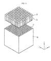
- FIG. 1 is an exploded perspective view illustrating a two-dimensional-array of an ultrasound probe according to an exemplary embodiment of the present disclosure
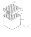
- FIG. 2 is an exploded perspective view illustrating a one-dimensional-array of an ultrasound probe according to an exemplary embodiment of the present disclosure.
- the ultrasound probe according to the exemplary embodiment includes a piezoelectric layer 20, a matching layer 10 disposed on a front-side surface of the piezoelectric layer 20, and a backing layer 30 disposed on a rear-side surface of the piezoelectric layer 20.
- a piezoelectric material generates a voltage in response to applied mechanical stress, and is mechanically deformed in response to an applied voltage. These effects are referred to as a piezoelectric effect and an inverse piezoelectric effect, respectively.
- a piezoelectric material is a material that converts electric energy into mechanical vibration energy, and vice versa.
- the ultrasound probe includes the piezoelectric layer 20 formed of a piezoelectric material(s) that generates an ultrasound by converting an applied electric signal into mechanical vibration.
- Examples of piezoelectric materials constituting the piezoelectric layer 20 may include at least one of lead zirconate titanate (PZT) ceramics, PZMT single crystals made of a solid solution of lead magnesium niobate and lead titanate, PZNT single crystals made of a solid solution of lead zinc niobate and lead titanate, or the like.
- PZT lead zirconate titanate
- the piezoelectric layer 20 may be arranged in either a single layer or a multilayered stack.
- the impedance and voltage of the piezoelectric layer 20 may be adjusted more easily, and better piezoelectric sensitivity, higher energy conversion efficiency and a smoother spectrum may be obtained.
- the matching layer 10 is disposed on the front-side surface of the piezoelectric layer 20.
- the matching layer 10 reduces a difference in acoustic impedance between the piezoelectric layer 20 and the subject to enable matching the acoustic impedance of the piezoelectric layer 20 with that of the subject, thereby allowing ultrasound generated by the piezoelectric layer 20 to be efficiently transferred to the subject.
- the matching layer 10 may be adapted to have a middle value between the acoustic impedances of the piezoelectric layer 20 and the subject.
- the matching layer 10 may be formed of a glass or resin material. Also, a plurality of matching layers 10 may be provided to allow the acoustic impedance to vary gradually from the piezoelectric layer 20 toward the subject, and each of the plurality of matching layers may be formed of a different material.
- the piezoelectric layer 20 and the matching layer 10 may be formed in a dicing process as a two-dimensional array in the shape of a matrix shown in FIG. 1 , or as a one-dimensional array shown in FIG. 2 .
- a protective layer may be disposed on a front-side surface of the matching layer 10.
- the protective layer may prevent high frequency signals generated by the piezoelectric layer 20 from being exposed to the outside and may block introduction of external high frequency signals.
- the protective layer may protect internal components from water and chemicals such as those used for disinfection, by applying or depositing a conductive material to the surface of a film with moisture-resistance and chemical resistance.
- a lens may be disposed on the front-side surface of the matching layer 10.
- the lens may be formed to be convex in a direction of irradiation of the ultrasonic waves to focus the ultrasonic waves, or may be formed to be concave in case the sound velocity is lower than in the subject.
- the backing layer 30, which is disposed on the rear-side surface of the piezoelectric layer 20, absorbs a portion of the ultrasonic waves generated in the piezoelectric layer 20 and traveling in a backward direction. This blocks the portion of the ultrasonic waves from being reflected in a forward direction, thereby preventing image distortion.
- a plurality of backing layers 30 may be provided.
- the backing layer 30 is also formed to have a plurality of grooves 31 arranged in a two-dimensional array, as shown in FIG. 1 .
- the number of grooves 31 may be equal to that of elements21 (see FIG. 4 ) constituting the two-dimensional array of the piezoelectric layer 20, and each of the grooves 31 may be formed to have the same or a similar cross-sectional shape as that of the corresponding element 21 so that the respective elements 21 may be seated in the grooves 31.
- the backing layer 30 is also formed to have a plurality of grooves 31 arranged in a one-dimensional array, as shown in FIG. 2 .
- the number of grooves 31 may be equal to that of elements 21 constituting the one-dimensional array of the piezoelectric layer 20, and each of the grooves 31 may be formed to have the same or a similar cross-sectional shape as that of the corresponding element 21 so that the respective elements 21 may be seated in the grooves 31.
- the depth of the grooves 31 may be set to allow the elements 21 to be stably seated while not degrading the efficiency of generating ultrasonic waves.
- the manufacturing technique used for forming the grooves 31 in the backing layer 30 is not limited. Various manufacturing techniques may be used depending on, for example, the shape of the grooves 31. For instance, in one exemplary process, the backing layer 30 provided with grooves 31 may be manufactured through casting.
- an adhesive When the elements 21 are installed in corresponding grooves 31, an adhesive, a silver epoxy, a conductive material, or the like, may be inserted between contact surfaces of the element 21 and the groove 31 for increasing accuracy in arranging the elements 21 to allow the elements 21 to be securely installed in the grooves 31.
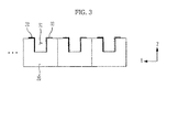
- FIG. 3 illustrates an example of conductive patterns 32 and 33 formed in the grooves 31 of the backing layer 30 of the ultrasound probe according to an exemplary embodiment of the present disclosure
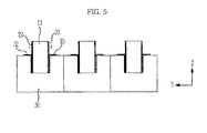
- FIG.'S 4 and 5 illustrate an example of a piezoelectric member which may be installed in the groove 31 in FIG. 3 and installation thereof in the groove 31, respectively
- FIG.'S 6 and 7 illustrate another example of a piezoelectric member which may be installed in the groove 31 in FIG. 3 and installation thereof in the groove 31, respectively.
- the piezoelectric member For the piezoelectric layer 20 to generate ultrasonic waves, an electric signal should be applied to the piezoelectric member constituting the piezoelectric layer 20. Therefore, the piezoelectric member is provided with electrodes 22 and 23, that is, a ground electrode 22 and a signal electrode 23, to which an electric signal is applied.
- the ground electrode 22 and signal electrode 23 are formed on each of the elements 21 constituting the array.
- conductive patterns 32 and 33 are formed in each of the grooves 31 in which the elements 21 are installed.
- the conductive patterns 32 and 33 may be formed to extend from both lateral sides of the groove 31 to outside the groove 31.
- the portions of the conductive patterns 32 and 33 extending outside the groove 31 may be electrically connected to an electric signal-supply member, for example, a printed circuit board (PCB) or a flexible printed circuit board (FPCB).
- PCB printed circuit board
- FPCB flexible printed circuit board
- the conductive patterns 32 and 33 extending toward each other from any two adjacent grooves 31 to the outside thereof may be formed to have different polarities.
- the conductive patterns 32 and 33 extending toward each other from the adjacent grooves 31 to the outside thereof are arranged not to contact each other.
- the conductive patterns 32 and 33 extending toward each other from any two adjacent grooves 31 to the outside thereof have the same polarity, that is, when both conductive patterns 32 and 33 contact the ground electrode 22 or both conductive patterns 32 and 33 contact the signal electrode 23, they may be connected to each other.
- the electric signals applied to the elements 21 need to be adjusted differently from each other, and thus the conductive patterns 32 and 33 formed by extending toward each other from the adjacent grooves 31 to the outside thereof may be provided with different polarities and arranged not to contact each other, as shown in FIG. 3 .
- FIG. 4 shows the piezoelectric member provided with the electrodes 22 and 23 adapted to be installed in the grooves 31.
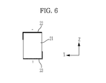
- the ground electrode 22 and signal electrode 23 may be formed on corresponding opposite lateral side surfaces of the element 21 as shown in FIG. 4 , so that when the element 21 is installed in the groove 31 (see FIG. 5 ), the ground electrode 22 and signal electrode 23 formed on the element 21 may contact the conductive patterns 32 and 33, respectively.
- the ground electrode 22 and signal electrode 23 may be formed only on the opposite lateral side surfaces of the element 21, or may further extend therefrom toward the front-side surface or rear-side surface of the element 21.
- ground electrode 22 and signal electrode 23 may be formed on the front-side and rear-side surfaces of the element 21 rather than on the opposite lateral side surfaces of the element 21 as shown in FIG. 13 .
- FIG. 6 shows the ground electrode 22 and signal electrode 23 formed on the front-side and rear-side surfaces of the element 21 and FIG. 7 illustrates installation of the element 21 of FIG. 6 in the groove 31.
- ground electrode 22 and signal electrode 23 When the ground electrode 22 and signal electrode 23 are formed on the front-side and rear-side surfaces of the element 21, they may extend toward opposite lateral side surfaces so that when the element 21 is installed in the groove 31, the ground electrode 22 and signal electrode 23 formed on the front-side and rear-side surfaces of the element 21, respectively, may contact the corresponding conductive patterns 32 and 33.
- FIG. 8 illustrates another example of conductive patterns 32 and 33 formed in the groove 31 of the backing layer 30 of the ultrasound probe according to an exemplary embodiment of the present disclosure
- FIG. 9 shows a piezoelectric member that may be installed in the grooves 31 of FIG. 8
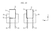
- FIG. 10 illustrates installation of the piezoelectric member of FIG. 9 in the grooves 31 of FIG. 8 .
- a bottom of the groove 31 may be provided with two conductive patterns 32 and 33 which are connected respectively to the ground electrode 22 and signal electrode 23.
- the conductive patterns 32 and 33 may be exposed at the bottom of the groove 31 and extend to a rear side of the backing layer 30 through an internal portion of the backing layer 30. At the rear side of the backing layer 30, the conductive patterns 32 and 33 may be connected to an external member supplying electrical signals.
- FIG. 9 shows the piezoelectric member provided with the ground electrode 22 and signal electrode 23 adapted to be installed in the grooves 31.
- the ground electrode 22 and signal electrode 23 may be formed on the element 21 as shown in FIG. 9 , so that when the element 21 is installed in the groove 31 (see FIG. 10 ), the ground electrode 22 and signal electrode 23 may contact the conductive patterns 32 and 33, respectively.
- the ground electrode 22 and signal electrode 23 are formed on the front-side and rear-side surfaces of the element 21, the ground electrode 22 is arranged on the rear-side surface and the signal electrode 23 on the front-side surface.
- the signal electrode 23 formed on the front-side surface of the element 21 may be arranged to extend to the rear-side surface of the element 21 along a lateral side surface of the element 21.
- the ground electrode 22 may be formed on the front-side surface of the element 21 and the signal electrode 23 formed on the rear-side surface of the element 21 as shown in, for example, FIG. 6 .
- ground electrode 22 and signal electrode 23 are formed on lateral side surfaces of the element 21, the ground electrode 22 and the signal electrode 23 may be respectively arranged on the opposite lateral side surfaces of element 21 and both may be arranged to extend to the rear-side surface of the element 21.
- one of the ground electrode 22 and signal electrode 23 may extend to a surface of the element 21 on which the other one of the ground electrode 22 and signal electrode 23 is formed, as shown in the example on the left in FIG. 9 .
- both the ground electrode 22 and signal electrode 23 may be formed to extend from the lateral side surfaces of the element 21 to the rear-side surface of the element 21 as shown in the example on the right in FIG. 9 , and in this case the conductive patterns 32 and 33 may be provided only at the bottom of the groove 31.
- ground electrode 22 and signal electrode 23 extending to the rear-side surface of the element 21 only need to be connected to the respective conductive patterns 32 and 33 formed on the bottom of the groove 31, they may be arranged to occupy as small an area of the rear-side surface of the element 21 as possible.
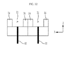
- FIG.'S 11 and 12 illustrate further examples of conductive patterns formed in the grooves 31 of the backing layer 30 of an ultrasound probe according to another embodiment of the present disclosure
- FIG. 13 shows a piezoelectric member that may be installed in the grooves 31 of FIG.'S 11 and 12.
- the backing layer 30 shown in FIG. 11 includes a backing member 34 provided with the grooves 31, a backing block 35 to support the backing member 34, and a conductive pattern 32 installed between the backing member 34 and the backing block 35.
- the conductive pattern 32 is electrically connected to an external member supplying electric signals and contacts one of the ground electrode 22 and signal electrode 23 of the element 21.
- conductive patterns 32 and 33 there are not two conductive patterns 32 and 33 formed to contact the ground electrode 22 and signal electrode 23, respectively, like the conductive patterns 32 and 33 in FIG.'S 3 and 8 described above, but one conductive pattern 32 is provided to contact only one of the ground electrode 22 and signal electrode 23.
- the conductive pattern 32 shown in FIG. 12 may be exposed at the bottom of the groove 31 to contact the ground electrode 22 of the element 21 to be installed in the groove 31, and may extend to the rear side of the backing layer 30 through the internal portion (e.g., backing block 35) of the backing layer 30. At the rear side of the backing layer 30, the conductive pattern 32 may be connected to an external member supplying electric signals.
- the conductive pattern 32 in FIG. 12 contacts one of the ground electrode 22 and signal electrode 23 of the element 21.
- FIG. 13 illustrates a piezoelectric member provided with the ground electrode 22 and signal electrode 23 to be installed in the grooves 31 in FIG.'S 11 and 12.
- the ground electrode 22 and signal electrode 23 formed on the element 21 may be arranged on the front-side and rear-side surfaces of the element 21 as shown in FIG. 13 , so that when the element 21 is installed in the groove 31, the one of the ground electrode 22 and signal electrode 23 may contact the conductive pattern 32.
- only the ground electrode 22 formed on the rear-side surface of the element 21 may receive an electric signal from the conductive pattern 32 formed in the groove 31.
- the signal electrode 23 formed on the front-side surface of the element 21 may receive an electric signal from a separate conductive pattern to be installed on the front-side surface of the piezoelectric member.
- the ground electrode 22 and signal electrode 23 may be formed only on the front-side and rear-side surfaces of the element 21, or may be arranged to extend from the front-side and rear-side surfaces to the opposite lateral side surfaces.
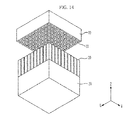
- FIG.'S 14 and 15 illustrate another exemplary embodiment of the present disclosure. That is, grooves 11 in which corresponding piezoelectric members are installed are formed in the matching layer 10 rather than in the backing layer 30.
- the matching layer 10 is formed to have a plurality of grooves 11 arranged in a two-dimensional array, as shown in FIG. 14 .
- the number of grooves 11 may be equal to that of the elements 21 constituting the two-dimensional array of the piezoelectric layer 20, and each of the grooves 31 may be formed to have the same or a similar cross-sectional shape as that of the corresponding element 21 so that the respective elements 21 may be installed in the grooves 31.
- the matching layer 10 is formed to have a plurality of grooves 11 arranged in a one-dimensional array, as shown in FIG. 15 .
- the number of grooves 11 may be equal to that of the elements 21 constituting the one-dimensional array of the piezoelectric layer 20, and each of the grooves 31 may be formed to have the same or a similar cross-sectional shape as that of the corresponding element 21 so that the respective elements 21 may be installed in the grooves 31.
- the depth of the grooves 11 may be set to allow the elements 21 to be stably seated while not degrading the efficiency of generating ultrasonic waves.
- the manufacturing technique used for forming the grooves 11 in the matching layer 10 is not limited. Various manufacturing techniques may be used depending on, for example, the shape of the grooves 11. For instance, in one exemplary process, the matching layer 10 provided with grooves 11 may be manufactured through casting.
- the orientation of the ground electrode 22 and signal electrode 23 formed on the elements 21 and the conductive patterns 32 and 33 formed in the grooves 11 are opposite to that defined in the exemplary embodiments illustrated in FIG.'S 3 to 13.
- the other details of the ground electrode 22 and signal electrode 23 and the conductive patterns 32 and 33 are the same as those for the embodiments illustrated in FIG.'S 3 to 13, and thus for the other details, refer to the description given above with respect to FIG.'S 3 to 13.
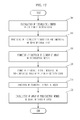
- FIG. 16 is a flowchart illustrating a manufacturing method of the ultrasound probe according to an exemplary embodiment of the present disclosure.
- the matching layer 10 is installed on one side of the piezoelectric member (100).
- the piezoelectric member and the matching layer 10 are processed into a one-dimensional or two-dimensional array (110).
- the array of the piezoelectric member may be formed through a dicing process. After the piezoelectric member is formed, it may have the shape shown in FIG.'S 1 and 2.
- the ground electrode 22 and signal electrode 23 are formed on each of the elements 21 constituting the array (120), the grooves 31 are provided on one side of the backing layer 30 in the same one-dimensional or two-dimensional array as that of the piezoelectric member (130), and then the conductive patterns 32 and 33 are formed in the grooves 31 (140).
- the grooves 31 to be formed on the backing layer 30 are also manufactured in a one-dimensional array. If the piezoelectric member is a two-dimensional array, the grooves 31 to be formed on the backing layer 30 are also manufactured in a two-dimensional array.
- the number of grooves 31 may be equal to that of the elements 21 constituting the array of the piezoelectric member, and each of the grooves 31 is formed to have the same or similar cross-sectional shape as that of the corresponding element 21.
- the manufacturing technique used for forming the grooves 31 in the backing layer 30 is not limited. Various manufacturing techniques may be used depending on, for example, the shape of the grooves 31. For instance, in one exemplary process, the backing layer 30 provided with grooves 31 may be manufactured through casting.
- the ground electrode 22 and signal electrode 23 are formed on each of the elements 21 constituting the array of the piezoelectric member, and the structure of the ground electrode 22 and signal electrode 23 is related to that of the conductive patterns 32 and 33 installed in the grooves 31 of the backing layer 30.
- the ground electrode 22 and signal electrode 23 formed on opposite lateral side surfaces of the element 21 may have various shapes. If the ground electrode 22 and signal electrode 23 are formed to extend from the front-side and rear-side surfaces of the element 21 to the opposite lateral side surfaces as shown in FIG. 6 , the conductive patterns 32 and 33 may be formed in the groove 31 of the backing layer 30 as shown in FIG. 3 or FIG. 7 .
- the ground electrode 22 and signal electrode 23 may be formed on the element 21 as shown in FIG. 9 , so that when the element 21 is installed in the groove 31, the ground electrode 22 and signal electrode 23 may contact the conductive patterns 32 and 33, respectively.
- the ground electrode 22 and signal electrode 23 are formed on the front-side and rear-side surfaces of the element 21, the ground electrode 22 is arranged on the rear-side surface and the signal electrode 23 on the front-side surface.
- the signal electrode 23 formed on the front-side surface of the element 21 may be arranged to extend to the rear-side surface of the element 21 along a lateral side surface of the element 21.
- the ground electrode 22 may be formed on the front-side surface of the element 21 and the signal electrode 23 formed on the rear-side surface of the element 21.
- ground electrode 22 and signal electrode 23 are formed on opposite lateral side surfaces of the element 21, the ground electrode 22 and the signal electrode 23 may be respectively arranged on the opposite lateral sides of element 21 and both may be arranged to extend to the rear-side surface of the element 21.
- the conductive pattern 32 may be formed in the groove 31 of the backing layer 30 as shown in FIG. 11 or FIG. 12 .
- the signal electrode 23 formed on the front-side surface of the element 21 may receive an electric signal from a separate conductive pattern to be installed on the front-side surface of the piezoelectric member.
- the array of the piezoelectric member is installed in the grooves 31 of the backing layer 30 (150).
- the array of the piezoelectric member should be installed such that the ground electrode 22 and signal electrode 23 formed on the elements 21 of the array contact the conductive patterns 32 and 33, respectively.
- an adhesive When the array of the piezoelectric member is installed in the grooves 31, an adhesive, a silver epoxy, a conductive material, or the like, may be inserted between contact surfaces of the element 21 and the groove 31 for increasing accuracy in arranging the elements 21 to allow the elements 21 to be securely installed in the grooves 31.
- FIG. 17 is a flowchart illustrating a manufacturing method of the ultrasound probe according to another exemplary embodiment of the present disclosure.
- the piezoelectric member is installed on one side of the backing layer (200).
- the piezoelectric member After being installed on one side of the backing layer, the piezoelectric member is processed into a one-dimensional or two-dimensional array (210).
- the piezoelectric member may be processed into an array through a dicing process. After the piezoelectric member is processed, it has the shape as shown in FIG.'S 14 and 15.
- the ground electrode 22 and signal electrode 23 are formed on each of the elements 21 constituting the array (220), the grooves 11 are formed on one side of the matching layer 10 in the same one-dimensional or two-dimensional array as that of the piezoelectric member (230), and then the conductive patterns 32 and 33 are formed in the grooves 11 (240).
- the grooves 11 to be formed in the matching layer 10 are also processed in a one-dimensional array. If the piezoelectric member is a two-dimensional array, the grooves 11 to be formed are also processed in a two-dimensional array.
- the number of grooves 11 may be equal to that of the elements 21 constituting the array of the piezoelectric member, and each of the grooves 11 is formed to have the same or similar cross-sectional shape as that of the corresponding element 21.
- the manufacturing technique used for forming the grooves 11 in the matching layer 10 is not limited. Various manufacturing techniques may be used depending on, for example, the shape of the grooves 11. For instance, in one exemplary process, the matching layer 10 provided with the grooves 11 may be manufactured through casting.
- the orientation of the ground electrode 22 and signal electrode 23 formed on the elements 21 and the conductive patterns 32 and 33 formed in the grooves 11 are opposite to that for the case in which the grooves 31 are formed in the backing layer 30.
- the other details of the ground electrode 22 and signal electrode 23 and the conductive patterns 32 and 33 are the same as those for the case in which the grooves 31 are formed in the backing layer 30, and thus for the other details, refer to the description given above with respect to FIG. 16 .
- the array of the piezoelectric member is installed in the grooves 11 of the matching layer 10 (250).
- an adhesive When the array of the piezoelectric member is installed in the grooves 11, an adhesive, a silver epoxy, a conductive material, or the like, may be inserted between contact surfaces of the element 21 and the groove 11 for increasing accuracy in arranging the elements 21 to allow the elements 21 to be securely installed in the grooves 11.
- an ultrasound probe and manufacturing method thereof may lower a defect rate and increase yield of ultrasound probes by improving the way the components of the ultrasound probe are connected to each other.
- the ultrasound probe and manufacturing method thereof may reduce crosstalk and provide a wider bandwidth and good sensitivity.
- grooves can be formed in the matching layer, convenient and various designs may be allowed.
Landscapes
- Health & Medical Sciences (AREA)
- Life Sciences & Earth Sciences (AREA)
- Engineering & Computer Science (AREA)
- Physics & Mathematics (AREA)
- Pathology (AREA)
- General Health & Medical Sciences (AREA)
- Surgery (AREA)
- Animal Behavior & Ethology (AREA)
- Veterinary Medicine (AREA)
- Public Health (AREA)
- Molecular Biology (AREA)
- Medical Informatics (AREA)
- Heart & Thoracic Surgery (AREA)
- Biomedical Technology (AREA)
- Biophysics (AREA)
- Nuclear Medicine, Radiotherapy & Molecular Imaging (AREA)
- Radiology & Medical Imaging (AREA)
- Mechanical Engineering (AREA)
- Gynecology & Obstetrics (AREA)
- Manufacturing & Machinery (AREA)
- Multimedia (AREA)
- Acoustics & Sound (AREA)
- General Physics & Mathematics (AREA)
- Chemical & Material Sciences (AREA)
- Biochemistry (AREA)
- Analytical Chemistry (AREA)
- Immunology (AREA)
- Transducers For Ultrasonic Waves (AREA)
- Ultra Sonic Daignosis Equipment (AREA)
- Investigating Or Analyzing Materials By The Use Of Ultrasonic Waves (AREA)
Applications Claiming Priority (1)
| Application Number | Priority Date | Filing Date | Title |
|---|---|---|---|
| KR1020120000105A KR101354603B1 (ko) | 2012-01-02 | 2012-01-02 | 초음파 프로브 및 그 제조방법 |
Publications (3)
| Publication Number | Publication Date |
|---|---|
| EP2610860A2 true EP2610860A2 (de) | 2013-07-03 |
| EP2610860A3 EP2610860A3 (de) | 2016-11-09 |
| EP2610860B1 EP2610860B1 (de) | 2018-11-28 |
Family
ID=47681551
Family Applications (1)
| Application Number | Title | Priority Date | Filing Date |
|---|---|---|---|
| EP12199703.5A Active EP2610860B1 (de) | 2012-01-02 | 2012-12-28 | Ultraschallsonde und Herstellungsverfahren dafür |
Country Status (5)
| Country | Link |
|---|---|
| US (1) | US9203012B2 (de) |
| EP (1) | EP2610860B1 (de) |
| JP (1) | JP2013141243A (de) |
| KR (1) | KR101354603B1 (de) |
| CN (1) | CN103181785B (de) |
Cited By (5)
| Publication number | Priority date | Publication date | Assignee | Title |
|---|---|---|---|---|
| EP2639789A3 (de) * | 2012-03-14 | 2014-02-26 | Samsung Electronics Co., Ltd | Mehrfach-Array-Ultraschallsondenvorrichtung und Verfahren zum Herstellen der Mehrfach-Array-Sondenvorrichtung |
| EP2902116A3 (de) * | 2014-01-14 | 2015-12-02 | Samsung Medison Co., Ltd. | Ultraschallsonde und Verfahren zur Herstellung davon |
| WO2015116340A3 (en) * | 2013-12-31 | 2015-12-03 | Acist Medical Systems, Inc. | Ultrasound transducer stack |
| US9530955B2 (en) | 2011-11-18 | 2016-12-27 | Acist Medical Systems, Inc. | Ultrasound transducer and processing methods thereof |
| EP2637166A3 (de) * | 2012-03-07 | 2017-12-20 | Samsung Medison Co., Ltd. | Ultraschallunterstützungselement, Wandler und Ultraschallsonde damit |
Families Citing this family (23)
| Publication number | Priority date | Publication date | Assignee | Title |
|---|---|---|---|---|
| US8805031B2 (en) * | 2008-05-08 | 2014-08-12 | Sonavation, Inc. | Method and system for acoustic impediography biometric sensing |
| US9877699B2 (en) | 2012-03-26 | 2018-01-30 | Teratech Corporation | Tablet ultrasound system |
| US10667790B2 (en) | 2012-03-26 | 2020-06-02 | Teratech Corporation | Tablet ultrasound system |
| KR101995867B1 (ko) * | 2012-07-12 | 2019-10-01 | 삼성전자주식회사 | 곡면프레임을 포함하는 트랜스듀서 모듈, 상기 트랜스듀서 모듈을 포함하는 초음파 프로브 및 상기 곡면프레임을 제조하는 방법 |
| US10074798B2 (en) | 2013-12-09 | 2018-09-11 | Samsung Medison Co., Ltd. | Method of manufacturing ultrasonic probe |
| KR102201866B1 (ko) * | 2014-01-07 | 2021-01-12 | 삼성메디슨 주식회사 | 초음파 프로브 |
| US20150196276A1 (en) * | 2014-01-14 | 2015-07-16 | Samsung Medison Co., Ltd. | Ultrasonic probe and method of manufacturing the same |
| KR102373132B1 (ko) * | 2014-12-26 | 2022-03-11 | 삼성메디슨 주식회사 | 초음파 프로브 장치 및 초음파 촬영 장치 |
| JP6608532B2 (ja) * | 2016-07-19 | 2019-11-20 | オリンパス株式会社 | 超音波プローブ、及び超音波内視鏡 |
| CN106824733A (zh) * | 2017-01-11 | 2017-06-13 | 上海爱声生物医疗科技有限公司 | 一种匹配层优化的超声换能器及其制作方法 |
| KR102658983B1 (ko) * | 2017-12-21 | 2024-04-18 | 제네럴 일렉트릭 컴퍼니 | 초음파 변환기 및 초음파 프로브 제조 방법 |
| CN108178121B (zh) * | 2018-02-07 | 2024-05-03 | 北京先通康桥医药科技有限公司 | 触诊探头及其制造方法 |
| JP6876645B2 (ja) * | 2018-03-15 | 2021-05-26 | 株式会社日立製作所 | 超音波プローブ及びその製造方法 |
| KR102135587B1 (ko) * | 2018-12-26 | 2020-07-20 | 동명대학교산학협력단 | 가스량 측정이 가능한 고감도 초음파 센서 |
| WO2021035022A1 (en) * | 2019-08-22 | 2021-02-25 | Farsounder, Inc. | Sonar transducer module with integrated protection |
| KR102304458B1 (ko) * | 2019-09-02 | 2021-09-24 | 한국파나메트릭스 주식회사 | 압전 단결정 소자를 이용한 초음파 센서 및 그 제조 방법 |
| KR20210105017A (ko) | 2020-02-18 | 2021-08-26 | 삼성메디슨 주식회사 | 초음파 프로브 및 그 제조 방법 |
| DE102021128282B4 (de) | 2021-10-29 | 2023-08-24 | Pi Ceramic Gmbh | Halterungsvorrichtung |
| KR102634238B1 (ko) * | 2021-11-26 | 2024-02-05 | 한국세라믹기술원 | 마이크로 초음파 트랜스듀서 어레이 및 이를 이용한 바이오 센서 패치 |
| KR102827333B1 (ko) * | 2022-12-02 | 2025-06-27 | 한국기계연구원 | 음향 메타렌즈를 포함하는 유연 센서, 이의 제조방법 및 이를 이용한 센싱방법 |
| KR102879201B1 (ko) * | 2023-03-28 | 2025-10-30 | 한국세라믹기술원 | 웨어러블 혈압 센서 |
| KR102896064B1 (ko) * | 2023-06-26 | 2025-12-04 | (주)아이블포토닉스 | 초음파 프로브 장치 |
| DE102023134663A1 (de) * | 2023-12-11 | 2025-06-12 | Pi Ceramic Gmbh | Aktuatorvorrichtung und Verfahren zur Herstellung einer Aktuatorvorrichtung |
Family Cites Families (16)
| Publication number | Priority date | Publication date | Assignee | Title |
|---|---|---|---|---|
| JPH0614397A (ja) * | 1991-11-30 | 1994-01-21 | Nippon Dempa Kogyo Co Ltd | 超音波探触子 |
| US5553035A (en) * | 1993-06-15 | 1996-09-03 | Hewlett-Packard Company | Method of forming integral transducer and impedance matching layers |
| US5630837A (en) * | 1993-07-01 | 1997-05-20 | Boston Scientific Corporation | Acoustic ablation |
| US6236144B1 (en) * | 1995-12-13 | 2001-05-22 | Gec-Marconi Limited | Acoustic imaging arrays |
| JP3649634B2 (ja) * | 1999-02-09 | 2005-05-18 | 東芝テック株式会社 | インクジェットプリンタヘッド及びその製造方法 |
| US6558323B2 (en) * | 2000-11-29 | 2003-05-06 | Olympus Optical Co., Ltd. | Ultrasound transducer array |
| US6540683B1 (en) * | 2001-09-14 | 2003-04-01 | Gregory Sharat Lin | Dual-frequency ultrasonic array transducer and method of harmonic imaging |
| JP4238103B2 (ja) | 2003-09-22 | 2009-03-11 | 富士フイルム株式会社 | 素子アレイの製造方法、及び、超音波トランスデューサアレイの製造方法 |
| US6856579B1 (en) * | 2003-09-29 | 2005-02-15 | The United States Of America As Represented By The Secretary Of The Navy | Broadband towed line array with spatial discrimination capabilities |
| JP2007282743A (ja) * | 2006-04-14 | 2007-11-01 | Toshiba Corp | 超音波プローブ、超音波プローブの製造方法及び超音波診断装置 |
| JP4253334B2 (ja) * | 2006-07-12 | 2009-04-08 | 株式会社東芝 | 2次元アレイ型超音波プローブ |
| JP4909115B2 (ja) * | 2007-02-21 | 2012-04-04 | 富士フイルム株式会社 | 超音波用探触子 |
| JP2008302044A (ja) * | 2007-06-08 | 2008-12-18 | Panasonic Corp | 超音波探触子とこれを用いた超音波診断装置および超音波探傷装置 |
| KR101137262B1 (ko) * | 2009-03-18 | 2012-04-20 | 삼성메디슨 주식회사 | 초음파 진단장치용 프로브 및 그 제조방법 |
| KR101137261B1 (ko) * | 2009-03-18 | 2012-04-20 | 삼성메디슨 주식회사 | 초음파 진단장치용 프로브 및 그 제조방법 |
| KR101145152B1 (ko) * | 2009-10-29 | 2012-05-15 | 삼성메디슨 주식회사 | 초음파 진단장치용 프로브 및 그 제조방법 |
-
2012
- 2012-01-02 KR KR1020120000105A patent/KR101354603B1/ko active Active
- 2012-12-28 JP JP2012288632A patent/JP2013141243A/ja active Pending
- 2012-12-28 EP EP12199703.5A patent/EP2610860B1/de active Active
- 2012-12-31 US US13/732,015 patent/US9203012B2/en active Active
-
2013
- 2013-01-04 CN CN201310001515.9A patent/CN103181785B/zh active Active
Non-Patent Citations (1)
| Title |
|---|
| None |
Cited By (8)
| Publication number | Priority date | Publication date | Assignee | Title |
|---|---|---|---|---|
| US9530955B2 (en) | 2011-11-18 | 2016-12-27 | Acist Medical Systems, Inc. | Ultrasound transducer and processing methods thereof |
| US10553776B2 (en) | 2011-11-18 | 2020-02-04 | Acist Medical Systems, Inc. | Ultrasound transducer and processing methods thereof |
| EP2637166A3 (de) * | 2012-03-07 | 2017-12-20 | Samsung Medison Co., Ltd. | Ultraschallunterstützungselement, Wandler und Ultraschallsonde damit |
| EP2639789A3 (de) * | 2012-03-14 | 2014-02-26 | Samsung Electronics Co., Ltd | Mehrfach-Array-Ultraschallsondenvorrichtung und Verfahren zum Herstellen der Mehrfach-Array-Sondenvorrichtung |
| US9071893B2 (en) | 2012-03-14 | 2015-06-30 | Samsung Electronics Co., Ltd. | Multi-array ultrasonic probe apparatus and method for manufacturing multi-array probe apparatus |
| WO2015116340A3 (en) * | 2013-12-31 | 2015-12-03 | Acist Medical Systems, Inc. | Ultrasound transducer stack |
| US9536511B2 (en) | 2013-12-31 | 2017-01-03 | Acist Medical Systems, Inc. | Ultrasound transducer stack |
| EP2902116A3 (de) * | 2014-01-14 | 2015-12-02 | Samsung Medison Co., Ltd. | Ultraschallsonde und Verfahren zur Herstellung davon |
Also Published As
| Publication number | Publication date |
|---|---|
| CN103181785B (zh) | 2016-12-07 |
| KR101354603B1 (ko) | 2014-01-23 |
| US9203012B2 (en) | 2015-12-01 |
| CN103181785A (zh) | 2013-07-03 |
| KR20130078935A (ko) | 2013-07-10 |
| EP2610860A3 (de) | 2016-11-09 |
| US20130169112A1 (en) | 2013-07-04 |
| JP2013141243A (ja) | 2013-07-18 |
| EP2610860B1 (de) | 2018-11-28 |
Similar Documents
| Publication | Publication Date | Title |
|---|---|---|
| US9203012B2 (en) | Ultrasound probe and manufacturing method thereof | |
| US20130181577A1 (en) | Ultrasonic probe and manufacturing method thereof | |
| US9445782B2 (en) | Ultrasonic probe and manufacturing method thereof | |
| US9073086B2 (en) | Probe for ultrasonic diagnostic apparatus and method of manufacturing the same | |
| KR101354605B1 (ko) | 초음파 프로브 및 그 제조방법 | |
| US10265051B2 (en) | Probe for ultrasonic imaging apparatus and method for manufacturing the same | |
| CN104720848B (zh) | 超声诊断设备及其制造方法 | |
| CN113331865B (zh) | 超声探头及制造超声探头的方法 | |
| CN108459085B (zh) | 超声探头 | |
| CN105726059B (zh) | 探头及其制造方法 | |
| EP3510934A1 (de) | Ultraschallsonde | |
| US9254119B2 (en) | Ultrasound probe and manufacturing method thereof |
Legal Events
| Date | Code | Title | Description |
|---|---|---|---|
| PUAI | Public reference made under article 153(3) epc to a published international application that has entered the european phase |
Free format text: ORIGINAL CODE: 0009012 |
|
| AK | Designated contracting states |
Kind code of ref document: A2 Designated state(s): AL AT BE BG CH CY CZ DE DK EE ES FI FR GB GR HR HU IE IS IT LI LT LU LV MC MK MT NL NO PL PT RO RS SE SI SK SM TR |
|
| AX | Request for extension of the european patent |
Extension state: BA ME |
|
| PUAL | Search report despatched |
Free format text: ORIGINAL CODE: 0009013 |
|
| AK | Designated contracting states |
Kind code of ref document: A3 Designated state(s): AL AT BE BG CH CY CZ DE DK EE ES FI FR GB GR HR HU IE IS IT LI LT LU LV MC MK MT NL NO PL PT RO RS SE SI SK SM TR |
|
| AX | Request for extension of the european patent |
Extension state: BA ME |
|
| RIC1 | Information provided on ipc code assigned before grant |
Ipc: G10K 11/00 20060101AFI20161006BHEP Ipc: B06B 1/06 20060101ALI20161006BHEP |
|
| 17P | Request for examination filed |
Effective date: 20170505 |
|
| RBV | Designated contracting states (corrected) |
Designated state(s): AL AT BE BG CH CY CZ DE DK EE ES FI FR GB GR HR HU IE IS IT LI LT LU LV MC MK MT NL NO PL PT RO RS SE SI SK SM TR |
|
| 17Q | First examination report despatched |
Effective date: 20180130 |
|
| REG | Reference to a national code |
Ref country code: DE Ref legal event code: R079 Ref document number: 602012054016 Country of ref document: DE Free format text: PREVIOUS MAIN CLASS: G10K0011000000 Ipc: B06B0001060000 |
|
| GRAP | Despatch of communication of intention to grant a patent |
Free format text: ORIGINAL CODE: EPIDOSNIGR1 |
|
| RIC1 | Information provided on ipc code assigned before grant |
Ipc: B06B 1/06 20060101AFI20180607BHEP Ipc: A61B 8/00 20060101ALI20180607BHEP Ipc: G10K 11/00 20060101ALI20180607BHEP |
|
| INTG | Intention to grant announced |
Effective date: 20180629 |
|
| GRAS | Grant fee paid |
Free format text: ORIGINAL CODE: EPIDOSNIGR3 |
|
| GRAA | (expected) grant |
Free format text: ORIGINAL CODE: 0009210 |
|
| AK | Designated contracting states |
Kind code of ref document: B1 Designated state(s): AL AT BE BG CH CY CZ DE DK EE ES FI FR GB GR HR HU IE IS IT LI LT LU LV MC MK MT NL NO PL PT RO RS SE SI SK SM TR |
|
| REG | Reference to a national code |
Ref country code: GB Ref legal event code: FG4D |
|
| REG | Reference to a national code |
Ref country code: CH Ref legal event code: EP |
|
| REG | Reference to a national code |
Ref country code: AT Ref legal event code: REF Ref document number: 1069622 Country of ref document: AT Kind code of ref document: T Effective date: 20181215 |
|
| REG | Reference to a national code |
Ref country code: DE Ref legal event code: R096 Ref document number: 602012054016 Country of ref document: DE |
|
| REG | Reference to a national code |
Ref country code: IE Ref legal event code: FG4D |
|
| REG | Reference to a national code |
Ref country code: LT Ref legal event code: MG4D Ref country code: NL Ref legal event code: FP |
|
| REG | Reference to a national code |
Ref country code: AT Ref legal event code: MK05 Ref document number: 1069622 Country of ref document: AT Kind code of ref document: T Effective date: 20181128 |
|
| PG25 | Lapsed in a contracting state [announced via postgrant information from national office to epo] |
Ref country code: AT Free format text: LAPSE BECAUSE OF FAILURE TO SUBMIT A TRANSLATION OF THE DESCRIPTION OR TO PAY THE FEE WITHIN THE PRESCRIBED TIME-LIMIT Effective date: 20181128 Ref country code: FI Free format text: LAPSE BECAUSE OF FAILURE TO SUBMIT A TRANSLATION OF THE DESCRIPTION OR TO PAY THE FEE WITHIN THE PRESCRIBED TIME-LIMIT Effective date: 20181128 Ref country code: NO Free format text: LAPSE BECAUSE OF FAILURE TO SUBMIT A TRANSLATION OF THE DESCRIPTION OR TO PAY THE FEE WITHIN THE PRESCRIBED TIME-LIMIT Effective date: 20190228 Ref country code: LV Free format text: LAPSE BECAUSE OF FAILURE TO SUBMIT A TRANSLATION OF THE DESCRIPTION OR TO PAY THE FEE WITHIN THE PRESCRIBED TIME-LIMIT Effective date: 20181128 Ref country code: LT Free format text: LAPSE BECAUSE OF FAILURE TO SUBMIT A TRANSLATION OF THE DESCRIPTION OR TO PAY THE FEE WITHIN THE PRESCRIBED TIME-LIMIT Effective date: 20181128 Ref country code: HR Free format text: LAPSE BECAUSE OF FAILURE TO SUBMIT A TRANSLATION OF THE DESCRIPTION OR TO PAY THE FEE WITHIN THE PRESCRIBED TIME-LIMIT Effective date: 20181128 Ref country code: BG Free format text: LAPSE BECAUSE OF FAILURE TO SUBMIT A TRANSLATION OF THE DESCRIPTION OR TO PAY THE FEE WITHIN THE PRESCRIBED TIME-LIMIT Effective date: 20190228 Ref country code: ES Free format text: LAPSE BECAUSE OF FAILURE TO SUBMIT A TRANSLATION OF THE DESCRIPTION OR TO PAY THE FEE WITHIN THE PRESCRIBED TIME-LIMIT Effective date: 20181128 Ref country code: IS Free format text: LAPSE BECAUSE OF FAILURE TO SUBMIT A TRANSLATION OF THE DESCRIPTION OR TO PAY THE FEE WITHIN THE PRESCRIBED TIME-LIMIT Effective date: 20190328 |
|
| PG25 | Lapsed in a contracting state [announced via postgrant information from national office to epo] |
Ref country code: GR Free format text: LAPSE BECAUSE OF FAILURE TO SUBMIT A TRANSLATION OF THE DESCRIPTION OR TO PAY THE FEE WITHIN THE PRESCRIBED TIME-LIMIT Effective date: 20190301 Ref country code: RS Free format text: LAPSE BECAUSE OF FAILURE TO SUBMIT A TRANSLATION OF THE DESCRIPTION OR TO PAY THE FEE WITHIN THE PRESCRIBED TIME-LIMIT Effective date: 20181128 Ref country code: PT Free format text: LAPSE BECAUSE OF FAILURE TO SUBMIT A TRANSLATION OF THE DESCRIPTION OR TO PAY THE FEE WITHIN THE PRESCRIBED TIME-LIMIT Effective date: 20190328 Ref country code: AL Free format text: LAPSE BECAUSE OF FAILURE TO SUBMIT A TRANSLATION OF THE DESCRIPTION OR TO PAY THE FEE WITHIN THE PRESCRIBED TIME-LIMIT Effective date: 20181128 Ref country code: SE Free format text: LAPSE BECAUSE OF FAILURE TO SUBMIT A TRANSLATION OF THE DESCRIPTION OR TO PAY THE FEE WITHIN THE PRESCRIBED TIME-LIMIT Effective date: 20181128 |
|
| PG25 | Lapsed in a contracting state [announced via postgrant information from national office to epo] |
Ref country code: PL Free format text: LAPSE BECAUSE OF FAILURE TO SUBMIT A TRANSLATION OF THE DESCRIPTION OR TO PAY THE FEE WITHIN THE PRESCRIBED TIME-LIMIT Effective date: 20181128 Ref country code: DK Free format text: LAPSE BECAUSE OF FAILURE TO SUBMIT A TRANSLATION OF THE DESCRIPTION OR TO PAY THE FEE WITHIN THE PRESCRIBED TIME-LIMIT Effective date: 20181128 Ref country code: CZ Free format text: LAPSE BECAUSE OF FAILURE TO SUBMIT A TRANSLATION OF THE DESCRIPTION OR TO PAY THE FEE WITHIN THE PRESCRIBED TIME-LIMIT Effective date: 20181128 |
|
| REG | Reference to a national code |
Ref country code: CH Ref legal event code: PL |
|
| REG | Reference to a national code |
Ref country code: DE Ref legal event code: R097 Ref document number: 602012054016 Country of ref document: DE |
|
| PG25 | Lapsed in a contracting state [announced via postgrant information from national office to epo] |
Ref country code: EE Free format text: LAPSE BECAUSE OF FAILURE TO SUBMIT A TRANSLATION OF THE DESCRIPTION OR TO PAY THE FEE WITHIN THE PRESCRIBED TIME-LIMIT Effective date: 20181128 Ref country code: RO Free format text: LAPSE BECAUSE OF FAILURE TO SUBMIT A TRANSLATION OF THE DESCRIPTION OR TO PAY THE FEE WITHIN THE PRESCRIBED TIME-LIMIT Effective date: 20181128 Ref country code: MC Free format text: LAPSE BECAUSE OF FAILURE TO SUBMIT A TRANSLATION OF THE DESCRIPTION OR TO PAY THE FEE WITHIN THE PRESCRIBED TIME-LIMIT Effective date: 20181128 Ref country code: LU Free format text: LAPSE BECAUSE OF NON-PAYMENT OF DUE FEES Effective date: 20181228 Ref country code: SK Free format text: LAPSE BECAUSE OF FAILURE TO SUBMIT A TRANSLATION OF THE DESCRIPTION OR TO PAY THE FEE WITHIN THE PRESCRIBED TIME-LIMIT Effective date: 20181128 Ref country code: SM Free format text: LAPSE BECAUSE OF FAILURE TO SUBMIT A TRANSLATION OF THE DESCRIPTION OR TO PAY THE FEE WITHIN THE PRESCRIBED TIME-LIMIT Effective date: 20181128 |
|
| REG | Reference to a national code |
Ref country code: IE Ref legal event code: MM4A |
|
| REG | Reference to a national code |
Ref country code: BE Ref legal event code: MM Effective date: 20181231 |
|
| PLBE | No opposition filed within time limit |
Free format text: ORIGINAL CODE: 0009261 |
|
| STAA | Information on the status of an ep patent application or granted ep patent |
Free format text: STATUS: NO OPPOSITION FILED WITHIN TIME LIMIT |
|
| GBPC | Gb: european patent ceased through non-payment of renewal fee |
Effective date: 20190228 |
|
| PG25 | Lapsed in a contracting state [announced via postgrant information from national office to epo] |
Ref country code: IE Free format text: LAPSE BECAUSE OF NON-PAYMENT OF DUE FEES Effective date: 20181228 Ref country code: SI Free format text: LAPSE BECAUSE OF FAILURE TO SUBMIT A TRANSLATION OF THE DESCRIPTION OR TO PAY THE FEE WITHIN THE PRESCRIBED TIME-LIMIT Effective date: 20181128 |
|
| 26N | No opposition filed |
Effective date: 20190829 |
|
| PG25 | Lapsed in a contracting state [announced via postgrant information from national office to epo] |
Ref country code: BE Free format text: LAPSE BECAUSE OF NON-PAYMENT OF DUE FEES Effective date: 20181231 |
|
| PG25 | Lapsed in a contracting state [announced via postgrant information from national office to epo] |
Ref country code: CH Free format text: LAPSE BECAUSE OF NON-PAYMENT OF DUE FEES Effective date: 20181231 Ref country code: LI Free format text: LAPSE BECAUSE OF NON-PAYMENT OF DUE FEES Effective date: 20181231 |
|
| PG25 | Lapsed in a contracting state [announced via postgrant information from national office to epo] |
Ref country code: MT Free format text: LAPSE BECAUSE OF NON-PAYMENT OF DUE FEES Effective date: 20181228 Ref country code: GB Free format text: LAPSE BECAUSE OF NON-PAYMENT OF DUE FEES Effective date: 20190228 |
|
| PGFP | Annual fee paid to national office [announced via postgrant information from national office to epo] |
Ref country code: NL Payment date: 20191217 Year of fee payment: 8 |
|
| PG25 | Lapsed in a contracting state [announced via postgrant information from national office to epo] |
Ref country code: TR Free format text: LAPSE BECAUSE OF FAILURE TO SUBMIT A TRANSLATION OF THE DESCRIPTION OR TO PAY THE FEE WITHIN THE PRESCRIBED TIME-LIMIT Effective date: 20181128 |
|
| PG25 | Lapsed in a contracting state [announced via postgrant information from national office to epo] |
Ref country code: MK Free format text: LAPSE BECAUSE OF NON-PAYMENT OF DUE FEES Effective date: 20181128 Ref country code: CY Free format text: LAPSE BECAUSE OF FAILURE TO SUBMIT A TRANSLATION OF THE DESCRIPTION OR TO PAY THE FEE WITHIN THE PRESCRIBED TIME-LIMIT Effective date: 20181128 Ref country code: HU Free format text: LAPSE BECAUSE OF FAILURE TO SUBMIT A TRANSLATION OF THE DESCRIPTION OR TO PAY THE FEE WITHIN THE PRESCRIBED TIME-LIMIT; INVALID AB INITIO Effective date: 20121228 |
|
| REG | Reference to a national code |
Ref country code: NL Ref legal event code: MM Effective date: 20210101 |
|
| PG25 | Lapsed in a contracting state [announced via postgrant information from national office to epo] |
Ref country code: NL Free format text: LAPSE BECAUSE OF NON-PAYMENT OF DUE FEES Effective date: 20210101 |
|
| PGFP | Annual fee paid to national office [announced via postgrant information from national office to epo] |
Ref country code: DE Payment date: 20251105 Year of fee payment: 14 |
|
| PGFP | Annual fee paid to national office [announced via postgrant information from national office to epo] |
Ref country code: IT Payment date: 20251106 Year of fee payment: 14 |
|
| PGFP | Annual fee paid to national office [announced via postgrant information from national office to epo] |
Ref country code: FR Payment date: 20251111 Year of fee payment: 14 |