EP2610898B1 - Procédé de fabrication d'un substrat épitaxial pour un dispositif semi-conducteur, et procédé de fabrication du dispositif semi-conducteur - Google Patents
Procédé de fabrication d'un substrat épitaxial pour un dispositif semi-conducteur, et procédé de fabrication du dispositif semi-conducteur Download PDFInfo
- Publication number
- EP2610898B1 EP2610898B1 EP11819859.7A EP11819859A EP2610898B1 EP 2610898 B1 EP2610898 B1 EP 2610898B1 EP 11819859 A EP11819859 A EP 11819859A EP 2610898 B1 EP2610898 B1 EP 2610898B1
- Authority
- EP
- European Patent Office
- Prior art keywords
- layer
- insulating layer
- barrier layer
- epitaxial substrate
- semiconductor device
- Prior art date
- Legal status (The legal status is an assumption and is not a legal conclusion. Google has not performed a legal analysis and makes no representation as to the accuracy of the status listed.)
- Not-in-force
Links
Images



Classifications
-
- H—ELECTRICITY
- H10—SEMICONDUCTOR DEVICES; ELECTRIC SOLID-STATE DEVICES NOT OTHERWISE PROVIDED FOR
- H10D—INORGANIC ELECTRIC SEMICONDUCTOR DEVICES
- H10D30/00—Field-effect transistors [FET]
- H10D30/40—FETs having zero-dimensional [0D], one-dimensional [1D] or two-dimensional [2D] charge carrier gas channels
- H10D30/47—FETs having zero-dimensional [0D], one-dimensional [1D] or two-dimensional [2D] charge carrier gas channels having two-dimensional [2D] charge carrier gas channels, e.g. nanoribbon FETs or high electron mobility transistors [HEMT]
-
- H—ELECTRICITY
- H10—SEMICONDUCTOR DEVICES; ELECTRIC SOLID-STATE DEVICES NOT OTHERWISE PROVIDED FOR
- H10D—INORGANIC ELECTRIC SEMICONDUCTOR DEVICES
- H10D30/00—Field-effect transistors [FET]
- H10D30/01—Manufacture or treatment
- H10D30/015—Manufacture or treatment of FETs having heterojunction interface channels or heterojunction gate electrodes, e.g. HEMT
-
- H—ELECTRICITY
- H10—SEMICONDUCTOR DEVICES; ELECTRIC SOLID-STATE DEVICES NOT OTHERWISE PROVIDED FOR
- H10D—INORGANIC ELECTRIC SEMICONDUCTOR DEVICES
- H10D30/00—Field-effect transistors [FET]
- H10D30/40—FETs having zero-dimensional [0D], one-dimensional [1D] or two-dimensional [2D] charge carrier gas channels
- H10D30/47—FETs having zero-dimensional [0D], one-dimensional [1D] or two-dimensional [2D] charge carrier gas channels having two-dimensional [2D] charge carrier gas channels, e.g. nanoribbon FETs or high electron mobility transistors [HEMT]
- H10D30/471—High electron mobility transistors [HEMT] or high hole mobility transistors [HHMT]
- H10D30/475—High electron mobility transistors [HEMT] or high hole mobility transistors [HHMT] having wider bandgap layer formed on top of lower bandgap active layer, e.g. undoped barrier HEMTs such as i-AlGaN/GaN HEMTs
-
- H—ELECTRICITY
- H10—SEMICONDUCTOR DEVICES; ELECTRIC SOLID-STATE DEVICES NOT OTHERWISE PROVIDED FOR
- H10D—INORGANIC ELECTRIC SEMICONDUCTOR DEVICES
- H10D30/00—Field-effect transistors [FET]
- H10D30/40—FETs having zero-dimensional [0D], one-dimensional [1D] or two-dimensional [2D] charge carrier gas channels
- H10D30/47—FETs having zero-dimensional [0D], one-dimensional [1D] or two-dimensional [2D] charge carrier gas channels having two-dimensional [2D] charge carrier gas channels, e.g. nanoribbon FETs or high electron mobility transistors [HEMT]
- H10D30/471—High electron mobility transistors [HEMT] or high hole mobility transistors [HHMT]
- H10D30/475—High electron mobility transistors [HEMT] or high hole mobility transistors [HHMT] having wider bandgap layer formed on top of lower bandgap active layer, e.g. undoped barrier HEMTs such as i-AlGaN/GaN HEMTs
- H10D30/4755—High electron mobility transistors [HEMT] or high hole mobility transistors [HHMT] having wider bandgap layer formed on top of lower bandgap active layer, e.g. undoped barrier HEMTs such as i-AlGaN/GaN HEMTs having wide bandgap charge-carrier supplying layers, e.g. modulation doped HEMTs such as n-AlGaAs/GaAs HEMTs
-
- H—ELECTRICITY
- H10—SEMICONDUCTOR DEVICES; ELECTRIC SOLID-STATE DEVICES NOT OTHERWISE PROVIDED FOR
- H10D—INORGANIC ELECTRIC SEMICONDUCTOR DEVICES
- H10D62/00—Semiconductor bodies, or regions thereof, of devices having potential barriers
- H10D62/80—Semiconductor bodies, or regions thereof, of devices having potential barriers characterised by the materials
- H10D62/82—Heterojunctions
- H10D62/824—Heterojunctions comprising only Group III-V materials heterojunctions, e.g. GaN/AlGaN heterojunctions
-
- H—ELECTRICITY
- H10—SEMICONDUCTOR DEVICES; ELECTRIC SOLID-STATE DEVICES NOT OTHERWISE PROVIDED FOR
- H10D—INORGANIC ELECTRIC SEMICONDUCTOR DEVICES
- H10D62/00—Semiconductor bodies, or regions thereof, of devices having potential barriers
- H10D62/80—Semiconductor bodies, or regions thereof, of devices having potential barriers characterised by the materials
- H10D62/85—Semiconductor bodies, or regions thereof, of devices having potential barriers characterised by the materials being Group III-V materials, e.g. GaAs
- H10D62/8503—Nitride Group III-V materials, e.g. AlN or GaN
-
- H—ELECTRICITY
- H10—SEMICONDUCTOR DEVICES; ELECTRIC SOLID-STATE DEVICES NOT OTHERWISE PROVIDED FOR
- H10P—GENERIC PROCESSES OR APPARATUS FOR THE MANUFACTURE OR TREATMENT OF DEVICES COVERED BY CLASS H10
- H10P14/00—Formation of materials, e.g. in the shape of layers or pillars
- H10P14/20—Formation of materials, e.g. in the shape of layers or pillars of semiconductor materials
- H10P14/24—Formation of materials, e.g. in the shape of layers or pillars of semiconductor materials using chemical vapour deposition [CVD]
-
- H—ELECTRICITY
- H10—SEMICONDUCTOR DEVICES; ELECTRIC SOLID-STATE DEVICES NOT OTHERWISE PROVIDED FOR
- H10P—GENERIC PROCESSES OR APPARATUS FOR THE MANUFACTURE OR TREATMENT OF DEVICES COVERED BY CLASS H10
- H10P14/00—Formation of materials, e.g. in the shape of layers or pillars
- H10P14/20—Formation of materials, e.g. in the shape of layers or pillars of semiconductor materials
- H10P14/29—Formation of materials, e.g. in the shape of layers or pillars of semiconductor materials characterised by the substrates
- H10P14/2901—Materials
-
- H—ELECTRICITY
- H10—SEMICONDUCTOR DEVICES; ELECTRIC SOLID-STATE DEVICES NOT OTHERWISE PROVIDED FOR
- H10P—GENERIC PROCESSES OR APPARATUS FOR THE MANUFACTURE OR TREATMENT OF DEVICES COVERED BY CLASS H10
- H10P14/00—Formation of materials, e.g. in the shape of layers or pillars
- H10P14/20—Formation of materials, e.g. in the shape of layers or pillars of semiconductor materials
- H10P14/29—Formation of materials, e.g. in the shape of layers or pillars of semiconductor materials characterised by the substrates
- H10P14/2901—Materials
- H10P14/2902—Materials being Group IVA materials
- H10P14/2904—Silicon carbide
-
- H—ELECTRICITY
- H10—SEMICONDUCTOR DEVICES; ELECTRIC SOLID-STATE DEVICES NOT OTHERWISE PROVIDED FOR
- H10P—GENERIC PROCESSES OR APPARATUS FOR THE MANUFACTURE OR TREATMENT OF DEVICES COVERED BY CLASS H10
- H10P14/00—Formation of materials, e.g. in the shape of layers or pillars
- H10P14/20—Formation of materials, e.g. in the shape of layers or pillars of semiconductor materials
- H10P14/32—Formation of materials, e.g. in the shape of layers or pillars of semiconductor materials characterised by intermediate layers between substrates and deposited layers
- H10P14/3202—Materials thereof
- H10P14/3214—Materials thereof being Group IIIA-VA semiconductors
- H10P14/3216—Nitrides
-
- H—ELECTRICITY
- H10—SEMICONDUCTOR DEVICES; ELECTRIC SOLID-STATE DEVICES NOT OTHERWISE PROVIDED FOR
- H10P—GENERIC PROCESSES OR APPARATUS FOR THE MANUFACTURE OR TREATMENT OF DEVICES COVERED BY CLASS H10
- H10P14/00—Formation of materials, e.g. in the shape of layers or pillars
- H10P14/20—Formation of materials, e.g. in the shape of layers or pillars of semiconductor materials
- H10P14/34—Deposited materials, e.g. layers
- H10P14/3402—Deposited materials, e.g. layers characterised by the chemical composition
- H10P14/3414—Deposited materials, e.g. layers characterised by the chemical composition being group IIIA-VIA materials
- H10P14/3416—Nitrides
Definitions
- the present invention relates to a method of manufacturing an epitaxial substrate having a multilayer structure made of a group-III nitride semiconductor, and particularly to a method of manufacturing an epitaxial substrate having a multilayer structure for use in a semiconductor device.
- a group-III nitride semiconductor is attracting attention as a semiconductor material for a next-generation high-frequency/high-power device, because the nitride semiconductor has a high breakdown electric field and a high saturation electron velocity.
- an HEMT (high electron mobility transistor) device in which a barrier layer made of AlGaN and a channel layer made of GaN are laminated takes advantage of the feature that causes a high-concentration two-dimensional electron gas (2DEG) to occur in a lamination interface (hetero interface) due to the large polarization effect (a spontaneous polarization effect and a piezo polarization effect) specific to a nitride material (for example, see Non-Patent Document 1).
- 2DEG high-concentration two-dimensional electron gas
- a single crystal (a different kind single crystal) having a composition different from that of a group-III nitride, such as silicon and SiC is used as a base substrate of an HEMT-device substrate.
- a buffer layer such as a strained-superlattice layer or a low-temperature growth buffer layer is generally formed as an initially-grown layer on the base substrate. Accordingly, a configuration in which a barrier layer, a channel layer, and a buffer layer are epitaxially formed on a base substrate is the most basic configuration of the HEMT-device substrate including a base substrate made of a different kind single crystal.
- a spacer layer having a thickness of about 1 nm may be sometimes provided between the barrier layer and the channel layer, for the purpose of facilitating a spatial confinement of the two-dimensional electron gas.
- the spacer layer is made of, for example, AlN.
- a cap layer made of, for example, an n-type GaN layer or a superlattice layer may be sometimes formed on the barrier layer, for the purpose of controlling the energy level at the most superficial surface of the HEMT-device substrate and improving contact characteristics of contact with an electrode.
- a nitride HEMT device has the most general configuration in which a channel layer is made of GaN and a barrier layer is made of AlGaN
- the concentration of a two-dimensional electron gas existing in an HEMT-device substrate increases as the AlN mole fraction in AlGaN of the barrier layer increases (for example, see Non-Patent Document 2). If the concentration of the two-dimensional electron gas can be considerably increased, the controllable current density of the HEMT device, that is, the power density that can be handled, would be considerably improved.
- an HEMT device having a structure with reduced strain such as an HEMT device in which a channel layer is made of GaN and a barrier layer is made of InAIN, in which the dependence on a piezo polarization effect is small and almost only a spontaneous polarization is used to generate a two-dimensional electron gas with a high concentration (for example, see Non-Patent Document 3).
- an electronic device and particularly a power semiconductor device that handles a power control, performs a normally-off operation, that is, an operation that blocks conduction when no electrical signal is not inputted from the outside.
- a normally-off operation that is, an operation that blocks conduction when no electrical signal is not inputted from the outside.
- an HEMT device made of a group-III nitride semiconductor is a device that uses a two-dimensional electron gas generated at a hetero interface as described above. Therefore, in an normally-on operation rather than the normally-off operation, the HEMT device originally exerts excellent conduction characteristics, that is, a low on-resistance.
- the following methods are known.
- a nitride HEMT device of Schottky gate structure type including a channel layer made of GaN and a barrier layer made of AlGaN for example, there are known: (1) a method in which the thickness of AlGaN barrier layer is reduced so that a gate threshold voltage (hereinafter, also referred to simply as a threshold voltage) is shifted in a positive direction, and thereby the normally-off is achieved (for example, see Non-Patent Document 4); and (2) a method in which recess etching is performed only in a portion immediately below a gate electrode (for example, see Non-Patent Document 5).
- a gate threshold voltage hereinafter, also referred to simply as a threshold voltage
- a channel layer is made of AlGaN whose Al mole fraction in all the group-III elements is 0.3 while a barrier layer is made of InAlGaN whose composition is in a predetermined composition range, to thereby achieve an HEMT device having a two-dimensional electron gas concentration of 2 ⁇ 10 13 /cm 2 or higher and capable of the normally-off operation (for example, see Patent Document 1).
- the reduction in the thickness of the barrier layer lowers the two-dimensional electron gas concentration.
- a low on-resistance which is the original feature of the nitride HEMT device, cannot be obtained.
- the reason therefor is considered as follows. As the thickness of the barrier layer decreases, the distance between a channel portion and a surface of the barrier layer decreases. As a result, the potential of a surface level contributes to generation of electric charges, or a piezo polarization effect is reduced.
- the adding of recess processing makes the process troublesome. To ensure the reproducibility in a device manufacturing process (to enable a device having a certain quality to be stably manufactured), a high accuracy of the recess processing is demanded.
- the methods (1) and (2) are directed to an HEMT device of Schottky gate structure type, in which an upper limit of a positive voltage that can be applied to the gate electrode is determined by the height of a Schottky barrier.
- a gate positive voltage is set to be about 1.5V or more, it is difficult to ensure a large drain current while suppressing a gate leakage current.
- the HEMT device has a feature that, when the HEMT device is designed to have a wide range of gate voltage application, a drain current thereof is increased. For example, in a case where the threshold voltage is -3V, the gate voltage range spans 4.5V, that is, from -3V to about +1.5V.
- the gate voltage range spans, at most, about 1.5V.
- a maximum drain current (on-current) of the former is about 0.8A/mm, that of the latter is about 0.4A/mm or less.
- the recess processing and the insulating film formation process are added, which makes the process troublesome.
- a high accuracy of the recess processing is demanded.
- the method (4) requires the step of forming the MIS gate structure. Moreover, the electron mobility in the inverted MIS channel structure is low, namely, 200cm 2 /Vs or less. Therefore, even when the normally-off operation is achieved, the performance of the HEMT device itself is degraded.
- Patent Document 1 International Patent Publication No. 2009/119357
- EP-A-1612866 discloses methods for manufacturing Group III-N field effect devices by convering the surface with a thin SiN layer on the top AlGaN layer.
- JP-A-2008-084942 discloses the use of an AlN insulating layer in the gate insulating layer of a MIS type FET, with an Si 3 N 4 insulating layer provided in the AlN insulating layer.
- the present invention has been made in view of the problems described above, and an object of the present invention is to provide a method for preparing a semiconductor device of normally-off operation type having a low on-resistance.
- a method of manufacturing an epitaxial substrate for semiconductor device is as set out in claim 1.
- the barrier layer is formed on the spacer layer.
- the spacer layer is made of AlN.
- a temperature T1(°C) at which the channel layer is formed is determined within a range of 950°C ⁇ T1 ⁇ 1250°C; and a temperature T2(°C) at which the barrier layer is formed is determined within a range of 800-667 ⁇ x2(°C) ⁇ T2 ⁇ 860-667 ⁇ x2(°C) and 600°C ⁇ T2 ⁇ 850°C, the range being determined in accordance with an InN mole fraction x2 in the second group-III nitride.
- a method of manufacturing a semiconductor device is as set out in claim 5.
- an epitaxial substrate having a high two-dimensional electron concentration and a low sheet resistance is achieved.
- Forming a semiconductor device by using such an epitaxial substrate achieves a semiconductor device of normally-off operation type having a low on-resistance in which a gate threshold voltage has a positive value and an upper limit of a gate voltage is high.
- the barrier layer having such a target composition can be surely formed.
- the semiconductor device can be prepared by using an epitaxial substrate having a high two-dimensional electron concentration and a low sheet resistance. Accordingly, a semiconductor device of normally-off operation type having a low on-resistance in which a gate threshold voltage has a positive value and an upper limit of a gate voltage is high can be achieved without performing a troublesome step of forming a recess gate structure.
- FIG. 1 is a schematic cross-sectional view showing an outline configuration of an HEMT device 20 that is one aspect of a semiconductor device that can be manufactured according to an embodiment of the present invention.
- the HEMT device 20 has a configuration in which a source electrode 7, a drain electrode 8, and a gate electrode 9 are arranged on an epitaxial substrate 10.
- the epitaxial substrate 10 has a configuration in which a base substrate 1, a buffer layer 2, a channel layer 3, a spacer layer 4, and a barrier layer 5 are laminated such that a (0001) crystal plane is substantially in parallel with a substrate surface. Additionally, an insulating layer 6 is formed on the barrier layer 5.
- the source electrode 7, the drain electrode 8, and the gate electrode 9 are formed on the insulating layer 6 of the epitaxial substrate 10.
- the thickness ratio among the layers shown in FIG. 1 does not reflect the actual ratio.
- all of the buffer layer 2, the channel layer 3, the spacer layer 4, the barrier layer 5, and the insulating layer 6 are epitaxially formed through a MOCVD process (Metal Organic Chemical Vapor Deposition) (details will be described later).
- MOCVD metal-organic chemical vapor deposition
- LPE liquid phase deposition processes
- the base substrate 1 No particular limitation is put on the base substrate 1, as long as the base substrate 1 allows a nitride semiconductor layer with good crystallinity to be formed thereon.
- a single crystal 6H-SiC substrate is used.
- a substrate made of sapphire, Si, GaAs, spinel, MgO, ZnO, ferrite, or the like, may be adopted.
- the buffer layer 2 is a layer made of AlN, and formed with a thickness of about several hundreds of nm, for the purpose of obtaining good crystal quality of the channel layer 3, the spacer layer 4, the barrier layer 5, and the insulating layer 6 which will be formed on the buffer layer 2.
- the buffer layer 2 is formed with a thickness of 200 nm.
- the composition of the barrier layer 5 is selected from a predetermined composition range in a ternary phase diagram for three components of InN, AlN, and GaN, as will be described later.
- the spacer layer 4 is provided between the channel layer 3 and the barrier layer 5.
- the spacer layer 4 is formed with a thickness of 0.5 nm to 1.5 nm.
- a two-dimensional electron gas region 3e in which the two-dimensional electron gas exists with a high concentration, is formed at an interface between the channel layer 3 and the spacer layer 4 (more specifically, in a portion of the channel layer 3 near this interface).
- the spacer layer 4 is provided in the epitaxial substrate 10. It may be also acceptable that the barrier layer 5 is formed directly on the channel layer 3. In this case, the two-dimensional electron gas region 3e is formed at an interface between the channel layer 3 and the barrier layer 5.
- an interface between the channel layer 3 and the spacer layer 4 immediately above the channel layer 3 or an interface between the channel layer 3 and the barrier layer 5 is formed such that the mean roughness of the interface is in the range from 0.1 nm to 3 nm.
- a surface of the spacer layer 4 or the barrier layer 5 is formed such that the mean square roughness of the surface is in the range from 0.1 nm to 3 nm.
- the above-mentioned mean roughness is in the range from 0.1 nm to 1 nm and the above-mentioned mean square roughness is in the range from 0.1 nm to 1 nm.
- an effect of confinement of the two-dimensional electron gas is further enhanced, to generate the two-dimensional electron gas with a higher concentration.
- the insulating layer 6 is a layer provided for the purpose of improving the characteristics of the epitaxial substrate 10 and the HEMT device 20.
- the insulating layer 6 includes a main insulating layer 6a serving as an uppermost layer of the epitaxial substrate 10, and a sub insulating layer 6b interposed between the barrier layer 5 and the main insulating layer 6a.
- the main insulating layer 6a is a layer made of silicon nitride (such as SiN), and formed with a thickness of 3 nm or less.
- the main insulating layer 6a is formed as a layer having a lower crystallinity than that of the ordinary insulating layer. This is achieved by setting a formation temperature at which the main insulating layer 6a is formed (i.e. the temperature of a susceptor of an MOCVD apparatus mentioned above) to be 750°C to 850°C, which is lower than an ordinary formation temperature (about 1000°C to 1200°C) adopted in a case where a silicon nitride layer is provided as the insulating layer.
- the main insulating layer 6a formed in this manner will be also referred to as a low-crystallinity insulating layer. Forming the low-crystallinity insulating layer as the main insulating layer 6a exerts an effect in suppression of a contact resistance of the HEMT device 20. Details thereof will be described later.
- the sub insulating layer 6b is a layer made of a group-III nitride having insulating properties, and formed with a thickness of 2.5 nm or less.
- the sub insulating layer 6b is laminated such that a (0001) crystal plane of the barrier layer 5 is substantially in parallel with the substrate surface.
- the sub insulating layer 6b is made of AlN, and preferably formed with a thickness of 2 nm or less. In an example not covered by the claims, only the main insulating layer 6a is formed as the insulating layer 6 on the barrier layer 5.
- Each of the source electrode 7 and the drain electrode 8 is a multilayer metal electrode whose metal layer has a thickness of about more than ten nm to one hundred and several tens of nm. Each of the source electrode 7 and the drain electrode 8 has an ohmic contact with the insulating layer 6.
- the source electrode 7 and the drain electrode 8 may be formed of a metal material that provides a good ohmic contact relative to the epitaxial substrate 10 (relative to the insulating layer 6). It is preferable that multilayer metal electrodes made of Ti/Al/Ni/Au are formed as the source electrode 7 and the drain electrode 8. However, this is not limiting. For example, a multilayer metal electrode made of Ti/Al/Pt/Au or Ti/Al may be formed.
- the formation of the source electrode 7 and the drain electrode 8 can be implemented through a photolithography process and a vacuum vapor deposition process.
- the gate electrode 9 is a single-layer or multilayer metal electrode in which one or more metal layers are formed with a thickness of more than ten nm to one hundred and several tens of nm.
- the gate electrode 9 forms an MIS interface between the gate electrode 9 and the barrier layer 5 via the insulating layer 6. It is preferable that the gate electrode 9 is made of, as a material, a metal having a high work function, such as Pd, Pt, Ni, and Au. Alternatively, it may be possible to form, as the gate electrode 9, a multilayer metal film consisted of some of the above-mentioned metals or concisted of some of the metals and Al, for example.
- the formation of the gate electrode 9 can be implemented through a photolithography process and a vacuum vapor deposition process.
- the HEMT device 20 can be considered as having an MIS gate structure.
- the composition of the barrier layer 5 is selected from a range that is enclosed by four straight lines represented by the following expressions for x2 and z2 in a ternary phase diagram for three components of InN, AlN, and GaN.
- a two-dimensional electron gas concentration in the two-dimensional electron gas region 3e of the epitaxial substrate 10 is 2 ⁇ 10 13 /cm 2 or more, and a threshold voltage of the HEMT device 20 is more than 0V.
- satisfying this composition range enables a high two-dimensional electron gas concentration to be maintained and the HEMT device 20 capable of a normally-off operation to be achieved.
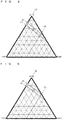
- the composition range of the barrier layer 5 indicated by the expressions (1) to (4) is shown on ternary phase diagrams for three components of InN, AlN, and GaN.
- the composition of the channel layer 3 is as follows.
- the channel layer 3 and the barrier layer 5 may contain impurities.
- the channel layer 3 and the barrier layer 5 may contain oxygen atoms within a concentration range from 0.0005 at% (1 ⁇ 10 17 /cm 3 ) or more to 0.05 at% (1 ⁇ 10 19 /cm 3 ) or less, or may contain carbon atoms within a concentration range from 0.0010at% (2 ⁇ 10 17 /cm 3 ) or more to 0.05at% (1 ⁇ 10 19 /cm 3 ) or less.
- the concentrations of oxygen atoms and carbon atoms may be below their respective lower limit values within the aforementioned ranges, this is not practical from the viewpoint of costs, the production yield, and the like.
- the concentrations of oxygen atoms and carbon atoms exceeding their respective upper limit values within the aforementioned ranges are not preferable, because the crystallinity of each layer is degraded to an extent that causes degradation of device characteristics.
- the spacer layer 4 is a layer provided for the purpose of enhancing the effect of confinement of the two-dimensional electron gas in the two-dimensional electron gas region 3e.
- the mobility of the two-dimensional electron gas in the HEMT device 20 is improved.
- the HEMT device 20 not including the spacer layer 4 has a mobility of about 300 to 400cm 2 /Vs, while the HEMT device 20 including the spacer layer 4 has a mobility of about 1000 to 1400cm 2 /Vs.
- the spacer layer 4 is formed with a thickness smaller than 0.5 nm, the formation is the layer is insufficient, and thus the effect of confinement of the two-dimensional electron gas is not sufficiently obtained.
- the spacer layer 4 is formed with a thickness greater than 1.5 nm, the film quality of the spacer layer 4 itself is degraded due to an internal stress, and thus sufficient improvement in the mobility cannot be expected.
- the spacer layer 4 also contains them with the same concentration range.
- the preparation of the epitaxial substrate 10 can be performed by using a known MOCVD apparatus. More specifically, an MOCVD apparatus is used that is configured to feed, into a reactor, a source gas (TMI, TMA, TMG) of an organic metal (MO) of In, Al, Ga, a silane gas that is a source gas of Si, an ammonia gas, a hydrogen gas, and a nitrogen gas.
- a source gas TMI, TMA, TMG
- a (0001)-oriented 6H-SiC substrate having a diameter of two inches is prepared as the base substrate 1, and this base substrate 1 is placed on a susceptor provided in a reactor of the MOCVD apparatus.
- the inside of the reactor is vacuumed, and then, an atmosphere in a hydrogen/nitrogen mixed flow state is created while a pressure inside the reactor is kept at a predetermined value in the range from 5 kPa to 50 kPa. In this condition, the susceptor is heated to thereby raise the temperature of the substrate.
- the temperature of the susceptor reaches a predetermined temperature in the range from 950°C to 1250°C (for example, 1050°C), which is a buffer layer formation temperature, an Al source gas and a NH 3 gas are introduced into the reactor, and thereby an AlN layer serving as the buffer layer 2 is formed.
- the channel layer formation temperature T1 is a value determined in a temperature range of 950°C ⁇ T1 ⁇ 1250°C in accordance with a value of an AlN mole fraction y1 in the channel layer 3.
- a pressure can be appropriately selected from the range from 10 kPa to an atmospheric pressure (100 kPa).
- a nitrogen gas atmosphere inside the reactor is maintained while the temperature of the susceptor is kept.
- the pressure in the reactor is set to be 10 kPa, and then a metal organic source gas and an ammonia gas are introduced into the reactor, so that an In x3 Al y3 Ga z3 N layer serving as the spacer layer 4 is formed with a predetermined thickness.
- the temperature of the susceptor is set to be 800°C or less. Therefore, it is necessary to lower the temperature of the susceptor after the formation of the spacer layer 4. In a case where no spacer layer 4 is provided, the surface of the channel layer 3 is exposed during the lowering of the temperature, which may cause the surface to be etched by an atmosphere gas. On the other hand, in a case where the spacer layer 4 is formed at a temperature substantially equal to the channel layer formation temperature T1, the temperature of the susceptor is lowered after the formation of the spacer layer 4. As a result, the spacer layer 4 acts as a protection layer that protects the surface of the channel layer 3. This would also contribute to improvement in the mobility of the two-dimensional electron gas.
- the temperature of the susceptor is kept at a predetermined barrier layer formation temperature T2(°C), and a nitrogen gas atmosphere is created within the reactor.
- the pressure inside the reactor is kept at a predetermined value (for example, 10 kPa) in the range from 1kPa to 30kPa.
- setting the pressure inside the reactor to be a predetermined value in the range from 1kPa to 20kPa achieves an HEMT device 20 having a low ohmic contact resistance and a less gate leakage current (having good Schottky contact characteristics). This effect derives from the fact that lowering the pressure in the reactor increases the surface flatness of the barrier layer 5.
- an ammonia gas and a metal organic source gas with a flow ratio in accordance with the composition of the barrier layer 5 are introduced into the reactor such that the so-called V/III ratio has a predetermined value of 3000 or more and 20000 or less is obtained.
- an In x2 Al y2 Ga z2 N layer serving as the barrier layer 5 is formed with a predetermined thickness.
- the In x2 Al y2 Ga z2 N layer is formed so as to having a composition that satisfies the expressions (1) to (4).
- a preferable range of the rate of growth of the barrier layer 5 is 0.01 to 0.1 ⁇ m/h.
- the formation is made such that the interface between the channel layer 3 and the barrier layer 5 has a mean roughness in the range from 0.1 nm to 1 nm and the surface of the barrier layer 5 has a mean square roughness in the range from 0.1 nm to 1 nm in a field of view of 5 ⁇ m ⁇ 5 ⁇ m.
- the barrier layer formation temperature T2 is in the range from 650°C or more to 800°C or less, and in a temperature range of 800-667 ⁇ x2(°C) ⁇ T2 ⁇ 860-667 ⁇ x2(°C), which is determined in accordance with an InN mole fraction x2 in the barrier layer 5.
- FIG. 6 is a diagram for explaining that the barrier layer formation temperature T2 is determined in the above-mentioned temperature range. That is, FIG. 6 is a diagram plotting the InN mole fraction x2 in the barrier layer 5 against the temperature of the susceptor, in a case where a ratio (hereinafter, In flow ratio) of the flow rate of the In source gas to the flow rate of the entire metal organic source gas is varied within the range from 0.5 or more to 0.8 or less, and the temperature of the susceptor (corresponding to the barrier layer formation temperature T2) at a time when the barrier layer 5 is formed is varied.
- the V/III ratio is set to be 5000.
- FIG. 6 reveals that data points are positioned on substantially the same straight line irrespective of the In flow ratio. This indicates that there is substantially a linear function relationship between the barrier layer formation temperature T2 and the InN mole fraction x2. Since there is no dependence on the In flow ratio, it is concluded that the InN mole fraction of the barrier layer is controllable by the barrier layer formation temperature T2 (the temperature of the susceptor) according to the above-mentioned functional relationship. That is, the barrier layer 5 having an aimed composition can be formed.
- the barrier layer formation temperature T2 can be determined from the above expression. Even in consideration of a variation caused by a difference among individual MOCVD apparatuses or individual heating members used for heating, the barrier layer 5 having a desired InN mole fraction x2 can be formed without fail by selecting a suitable temperature in a range of ⁇ 30°C from the above expression.
- the barrier layer 5 can be formed so as to have excellent controllability in a wide composition range, for example, in the composition range determined by the above-mentioned expressions (1) to (4).
- a nitrogen gas is used for all of a bubbling gas of a metal organic source and a carrier gas. That is, an atmosphere gas other than the source gas is only the nitrogen gas. Accordingly, the hydrogen-terminated dangling bond can be made nitrogen-terminated, and an electron structure of the barrier layer 5 is maintained in an ideal state, with the result that the generation of the two-dimensional electron gas in the two-dimensional electron gas region 3e is achieved with a high concentration. Note that it is not preferable to intentionally mix a hydrogen gas into the atmosphere during the preparation of the barrier layer 5, because this causes a reduction in the two-dimensional electron gas concentration.
- the temperature of the susceptor is set to be a predetermined sub insulating layer formation temperature.
- an Al source gas and a NH 3 gas are introduced into the reactor, and thereby an AlN layer serving as the sub insulating layer 6b is formed with a predetermined thickness.
- the temperature of the susceptor is set to be a main insulating layer formation temperature that is 750°C or more and 850°C or less (for example, 800°C).
- a silane gas and a NH 3 gas are introduced into the reactor, and thereby a silicon nitride layer serving as the main insulating layer 6a is formed with a predetermined thickness.
- the main insulating layer formation temperature is set lower than an ordinary formation temperature that is adopted in a case where a silicon nitride layer is provided as an insulating layer.
- Forming the main insulating layer 6a at a temperature higher than 850°C is not preferable, because this increases a contact resistance of the HEMT device 20.
- setting the main insulating layer formation temperature to be below 750°C is not preferable, because this makes it difficult to form the main insulating layer 6a itself through a MOCVD process.
- the preparation of the epitaxial substrate 10 is completed. After the epitaxial substrate 10 is obtained, this is used to prepare the HEMT device 20. Subsequent steps are achieved through a known method.
- a device isolation step is performed for etching and removing portions that will be boundaries between individual devices through a photolithography process and an RIE process into a depth of about 400 nm.
- This device isolation step is a step necessary for obtaining a large number of HEMT devices 20 from one epitaxial substrate 10, and essentially not necessary for the present invention.
- a SiO 2 film having a predetermined thickness (for example, 10 nm) is formed on the epitaxial substrate 10. Then, through a photolithography process, the SiO 2 film only in expected formation positions where the source electrode 7 and the drain electrode 8 are to be formed is removed by etching. Thereby, a SiO 2 pattern layer is formed.
- the source electrode 7 and the drain electrode 8 made of Ti/Al/Ni/Au are formed at their expected formation positions. Then, a heat treatment is performed for several tens of seconds (for example, 30 seconds) in the nitrogen gas atmosphere at a predetermined temperature (for example, 800°C) in the range from 650°C to 1000°C. As a result of this heat treatment, metal elements of the electrodes are alloyed, and diffused to transmit through the main insulating layer 6a. This ensures suitable ohmic characteristics of the source electrode 7 and the drain electrode 8 relative to the barrier layer 5.
- a predetermined temperature for example, 800°C
- the SiO 2 film in an expected formation position where the gate electrode 9 is to be formed is removed from the SiO 2 pattern layer through a photolithography process. Then, through a vacuum vapor deposition process and a photolithography process, the gate electrode 9 made of Ni/Au is formed in this expected formation position.
- the remaining portion of the SiO 2 pattern layer is removed. Then, a resultant is singulated into chips each having a predetermined size. Thereby, a large number of HEMT devices 20 are obtained. On the HEMT device 20 thus obtained, die bonding and wire bonding are performed as appropriate.
- the HEMT device 20 thus obtained is subjected to a heat treatment for the purpose of improving a mechanical strength of a bonding portion between the gate electrode 9 and the epitaxial substrate 10 (for the purpose of preventing peeling of the gate electrode 9).
- this heat treatment is performed by holding the HEMT device 20 for several tens of seconds in a nitrogen gas atmosphere at a predetermined temperature in the range from 500°C to 900°C.
- the epitaxial substrate 10 according to this embodiment in which the compositions of the channel layer 3 and the barrier layer 5 are determined in the above-mentioned composition ranges, is structured such that it is less influenced by a surface level and such that a spontaneous polarization effect makes more contribution than a piezo effect.
- the inventors has confirmed that, as compared with a structure (AlGaN/GaN structure) in which the channel layer 3 is made of GaN and the barrier layer is made of AlGaN, a high two-dimensional electron gas concentration is maintained and a sheet resistance is kept low, even when the thickness of the barrier layer is reduced.
- the main insulating layer 6a is formed in the above-described manner, and therefore a surface level is controlled. This exerts effects that a high two-dimensional electron gas concentration is maintained and the sheet resistance is further reduced. For example, in the epitaxial substrate 10, the sheet resistance is reduced down to about 1/2, as compared with a case where no main insulating layer 6a is provided.
- both the thickness of the barrier layer 5 and the thickness of the main insulating layer 6a are 3 nm or less, but nevertheless a high two-dimensional electron gas concentration and a low sheet resistance are maintained. Therefore, in the HEMT device 20 prepared by using the epitaxial substrate 10, a normally-off state is achieved only by a built-in potential of a portion corresponding to the gate electrode 9. The following fact also contributes to the achievement of the normally-off state.
- the main insulating layer 6a made of silicon nitride is bonded to the barrier layer 5 with a sufficiently small thickness made of a group-III nitride having a composition of In x2 Al y2 Ga z2 N, so that a conduction band edge of the barrier layer 5 is, throughout the entire film thickness thereof, pushed up toward a high energy side.
- the thickness of the main insulating layer 6a reduces a threshold voltage.
- the threshold voltage is negative, so that the normally-off operation is not achieved.
- the main insulating layer 6a is formed as a layer with a low crystallinity. This exerts an effect that, in the heat treatment performed after the formation of the pattern of the source electrode 7 and the drain electrode 8, the diffusion and transmission of metal elements of these electrodes in the main insulating layer 6a is suitably provoked.
- the HEMT device 20 even though the source electrode 7 and the drain electrode 8 are formed on the main insulating layer 6a, the ohmic characteristics of these electrodes are sufficiently ensured. As a result, the contact resistance is suppressed.
- a contact resistance of an epitaxial substrate whose main insulating layer 6a is formed at 900°C is two orders higher than the contact resistance of the epitaxial substrate 10 according to this embodiment whose main insulating layer 6a is formed at a temperature in the range from 750°C to 850°C.
- Providing the sub insulating layer 6b in addition to the main insulating layer 6a exerts an effect that the gate leakage current is reduced in the HEMT device 20.
- a thickness equal to or greater than 3 nm is not preferable, because it causes the threshold voltage to be negative, thus failing to achieve the normally-off operation, and it also increases the contact resistance.
- the HEMT device 20 has the MIS gate structure. This can ensure a higher upper limit of a gate voltage range, as compared with a HEMT device of Schottky type in which an upper limit of the gate positive voltage is limited by the height of the Schottky barrier. That is, the gate voltage range can be enlarged as compared with the HEMT device of Schottky type. As a result, a drain current can be increased. Additionally, a gate junction is substantially an MIS junction, and therefore the leakage current is reduced in both cases where the gate bias is positive and negative.
- this embodiment achieves an HEMT device of normally-off operation type having excellent characteristics without performing a troublesome step of forming a recess gate structure. This does not exclude that the source electrode 7 and the drain electrode 8 have recess structures.
- the main insulating layer 6a made of silicon nitride is formed continuously from the layer (the sub insulating layer 6b or the barrier layer 5) located immediately below. Therefore, a reduction in drain-current collapse, and the like, are expected.
- a barrier layer is formed with a thickness of 3 nm or less so as to satisfy the above-mentioned composition range, and a (main) insulating layer made of silicon nitride is formed with a thickness of 3 nm or less at a formation temperature of 750°C to 850°C.
- an HEMT device of normally-off operation type having a low on-resistance, in which the gate threshold voltage has a positive value and the upper limit of the gate voltage is high, can be achieved without performing a troublesome step of forming a recess gate structure.
- each of the types of epitaxial substrates 10 was measured for its sheet resistance.
- each epitaxial substrate 10 was used to prepare an HEMT device 20, and its threshold voltage, contact resistance, and gate leakage current were evaluated.
- Table 1 shows a list of formation conditions specific to and measurement results of specimens (specimen Nos. a-1 to a-18) in which the channel layer 3 was made of GaN and the barrier layer 5 was made of In 0.23 Al 0.77 N.
- Table 2 shows a list of formation conditions specific to and measurement results of specimens (specimen Nos. b-1 to b-18) in which the channel layer 3 is made of Al 0.2 Ga 0.8 N and the barrier layer 5 is made of In 0.154 Al 0.646 Ga 0.2 N.
- the epitaxial substrate 10 was prepared. At that time, until the formation of the barrier layer 5, all the epitaxial substrates 10 were prepared under the same conditions except the above-mentioned conditions.
- a plurality of (0001)-oriented 6H-SiC substrates having a diameter of two inches were prepared as the base substrate 1.
- the thickness thereof was 300 ⁇ m.
- Each of the substrates was placed in a reactor of an MOCVD apparatus, and the inside of the reactor was vacuumed. Then, the pressure in the reactor was set to be 30 kPa, and an atmosphere in a hydrogen/nitrogen mixed flow state was created. Then, the susceptor was heated, to thereby raise the temperature of the base substrate 1.
- a TMA bubbling gas and an ammonia gas were introduced into the reactor, and an AlN layer having a thickness of 200 nm was formed as the buffer layer.
- the temperature of the susceptor was set to be a predetermined temperature
- a TMG bubbling gas serving as the metal organic source gas and an ammonia gas were introduced into the reactor with a predetermined flow ratio.
- a GaN layer or Al 0.2 Ga 0.8 N layer serving as the channel layer 3 was formed with a thickness of 2 ⁇ m.
- the pressure in the reactor was set to be 10 kPa, and then a TMA bubbling gas and an ammonia gas were introduced into the reactor.
- a TMA bubbling gas and an ammonia gas were introduced into the reactor.
- an AlN layer having a thickness of 1 nm was formed as the spacer layer 4.
- the barrier layer 5 was then formed.
- the temperature of the susceptor was set in accordance with the composition of the barrier layer.
- the thickness of the barrier layer 5 was varied in four levels of 2 nm, 2.5 nm, 3 nm, and 4 nm.
- an AlN layer serving as the sub insulating layer 6b was formed.
- the thickness of the sub insulating layer 6b was varied in five levels of 0 nm (corresponding to a case where no sub insulating layer 6b is provided), 1 nm, 2 nm, 2.5 nm, and 3 nm. In any of the cases, the temperature of the susceptor was 1050°C.
- a silicon nitride layer serving as the main insulating layer 6a was formed.
- the thickness of the main insulating layer 6a was varied in six levels of 0 nm (corresponding to a case where no main insulating layer 6a is provided), 1.5 nm, 2 nm, 2.5 nm, 3 nm, and 4 nm.
- the temperature of the susceptor was varied in five levels of 750°C, 800°C, 850°C, 900°C, and 1000°C.
- the temperature of the susceptor was lowered to the vicinity of a room temperature, and the inside of the reactor was returned to the atmospheric pressure. Then, the prepared epitaxial substrates 10 were taken out. Through the above-described procedures, each of the epitaxial substrates 10 was obtained.
- the obtained epitaxial substrates 10 were measured for their sheet resistances by the four-terminal method. The results thus obtained were shown in Table 1 and Table 2.
- an electrode pattern made of Ti/Al/Ni/Au (with film thicknesses of 25/75/15/100 nm, respectively) was formed on an upper surface of the main insulating layer 6a in expected formation positions where the source electrode 7 and the drain electrode 8 were to be formed. Then, a heat treatment was performed in nitrogen for 30 seconds at 800°C.
- a pattern of the gate electrode 9 made of Ni/Au (with a film thickness of 6 nm/12 nm) was formed on the upper surface of the main insulating layer 6a in an expected formation position where the gate electrode 9 was to be formed.
- the gate electrode 9 was formed such that its portion bonded to the main insulating layer 6a has a size of 1mm ⁇ 1mm.
- the gate leakage currents of the specimens including the main insulating layer 6a were reduced to about 1/10000 to 1/1000000 of the gate leakage currents of the specimens not including the main insulating layer 6a. This indicates that preparing the HEMT device 20 by using the epitaxial substrate 10 that includes the main insulating layer 6a is highly effective in a reduction in the gate leakage current of the HEMT device 20.
- the contact resistances of the specimens (a-10, a-11, b-10, b-11) having a formation temperature of 900°C or more were about two orders higher than the contact resistances of the other specimens having a formation temperature of 800°C or less. This result indicates that lowering the formation temperature to thereby form the main insulating layer 6a as a layer having a lower crystallinity than that of an ordinary insulating layer is effective in a reduction in the contact resistance.
- the gate leakage currents thereof were lower than the gate leakage currents of the specimens (a-3, a-4, b-3, b-4) not including the sub insulating layer 6b in which the barrier layer 5 and the main insulating layer 6a were prepared under the same preparation conditions.
- the threshold voltages were negative and the contact resistances were increased.
- the sub insulating layer 6b with a thickness of 3 nm or less is effective in a reduction in the gate leakage current of the HEMT device 20.
- the thickness of the sub insulating layer 6b is 2 nm or less.
- each of the types of epitaxial substrates 10 thus obtained was measured for its sheet resistance.
- each epitaxial substrate 10 was used to prepare an HEMT device 20, and its threshold voltage, contact resistance, and gate leakage current were evaluated.
- the thickness of the barrier layer 5 was 2 nm.
- the thickness of the main insulating layer 6a was 2 nm and the formation temperature (the temperature of the susceptor) at which the main insulating layer 6a was formed was 800°C.
- the sub insulating layer 6b was not formed. Table 3 shows a list of formation conditions specific to and measurement results of the specimens.
- compositions of the barrier layers 5 of the respective specimens were plotted with circles. That is, the compositions of the channel layers 3 and the barrier layers 5 of all the specimens were including in a range that is enclosed by four straight lines represented by the expressions (1) to (4). [Table 3] No.
- Table 3 The results shown in Table 3 indicate that preparing an epitaxial substrate by selecting the compositions of the channel layer 3 and the barrier layer 5 from the composition ranges represented by the expressions (1) to (4) can achieve an epitaxial substrate having a low sheet resistance, and that preparing an HEMT device by using this epitaxial substrate as described in the embodiment above can achieve an HEMT device of normally-off operation type having a low on-resistance in which the gate threshold voltage has a positive value and the upper limit of the gate voltage is high.
Landscapes
- Junction Field-Effect Transistors (AREA)
- Formation Of Insulating Films (AREA)
- Thin Film Transistor (AREA)
- Insulated Gate Type Field-Effect Transistor (AREA)
Claims (5)
- Procédé de fabrication d'un substrat épitaxial (10) pour dispositif à semi-conducteur (20), ledit procédé comprenant :une étape de formation de couche de canal de formation épitaxiale d'une couche de canal (3) sur un substrat de base (1), ladite couche de canal étant constituée d'un premier nitrure du groupe III ayant une composition de Inx1Aly1Gaz1N, où x1+y1+z1=1, qui contient au moins Ga ;une étape de formation de couche barrière de formation épitaxiale d'une couche barrière (5) sur ladite couche de canal (3), ladite couche barrière étant constituée d'un deuxième nitrure du groupe III ayant une composition de Inx2Aly2Gaz2N, où x2+y2+z2=1, qui contient au moins In et Al ; dans lequeldans ladite étape de formation de couche de canal, la composition dudit premier nitrure du groupe III est choisie dans une plage déterminée par x1=0 et 0≤y1≤0,3,dans ladite étape de formation de couche barrière,la composition dudit deuxième nitrure du groupe III est sélectionnée, dans un diagramme de phase ternaire pour InN, AIN et GaN, dans une plage qui est délimitée par des lignes droites représentées par les expressions suivantes pour x2 et z2 et qui est déterminée en fonction de la composition dudit premier nitrure du groupe III, etladite couche barrière (5) est formée avec une épaisseur de 3 nm ou moins,dans lequel les expressions pour x2 et z2 sont :


une étape de formation de couche isolante principale de formation d'une couche isolante principale (6a) sur ladite couche barrière (5), ladite couche isolante principale étant constituée de nitrure de silicium,
dans lequel, dans ladite étape de formation de couche isolante principale, ladite couche isolante principale (6a) est formée avec une épaisseur de 3 nm ou moins par MOCVD à une température de formation de 750 °C ou plus et 850 °C ou moins, le procédé comprenant en outre :
une étape de formation de sous-couche isolante de formation épitaxiale d'une sous-couche isolante (6b) sur ladite couche barrière (5), ladite sous-couche isolante étant constituée d'un nitrure du groupe III ayant des propriétés isolantes et ayant une épaisseur de 2,5 nm ou moins, dans lequel ladite couche isolante principale (6a) est formée sur ladite sous-couche isolante (6b), et dans lequel ladite sous-couche isolante (6b) est constituée d'AIN. - Procédé de fabrication d'un substrat épitaxial pour dispositif à semi-conducteur selon la revendication 1, comprenant en outre :une étape de formation de couche d'espacement de formation d'une couche d'espacement (4) sur ladite couche de canal (3), ladite couche d'espacement étant constituée d'un troisième nitrure du groupe III ayant une composition de Inx3Aly3Gaz3N, où x3+y3+z3=1, qui contient au moins Al et qui a une énergie de bande interdite plus élevée que celle de ladite couche barrière, dans lequelladite couche barrière (5) est formée sur ladite couche d'espacement (4).
- Procédé de fabrication d'un substrat épitaxial pour dispositif à semi-conducteur selon la revendication 2, dans lequel
ladite couche d'espacement (4)est constituée d'AIN. - Procédé de fabrication d'un substrat épitaxial pour dispositif à semi-conducteur selon l'une quelconque des revendications 1 à 3, dans lequel
une température T1 à laquelle ladite couche de canal (3) est formée est déterminé dans une plage de 950 °C≤T1≤1250 °C,
une température T2 à laquelle ladite couche barrière (5) est formée est déterminée dans une plage de 800-667·x2≤T2≤860-667·x2 et 600 °C≤T2≤850 °C, ladite plage étant déterminée en fonction d'une fraction molaire d'InN x2 dans ledit deuxième nitrure du groupe III, dans lequel T1 et T2 sont exprimés en °C. - Procédé de fabrication d'un dispositif à semi-conducteur (20), ledit procédé comprenant les étapes de :préparation d'un substrat épitaxial (10) selon le procédé de fabrication d'un substrat épitaxial pour dispositif à semi-conducteur selon l'une quelconque des revendications 1 à 4 ;formation d'une électrode de source (7) et d'une électrode de drain (8) sur ladite couche isolante principale dudit substrat épitaxial ;conduite d'un traitement thermique sur ledit substrat épitaxial comportant ladite électrode de source et ladite électrode de drain formées sur celui-ci pour former une jonction ohmique ; etformation d'une électrode de grille (9) sur ladite couche isolante principale (6a), avec une jonction MIS.
Applications Claiming Priority (2)
| Application Number | Priority Date | Filing Date | Title |
|---|---|---|---|
| JP2010187899 | 2010-08-25 | ||
| PCT/JP2011/068742 WO2012026396A1 (fr) | 2010-08-25 | 2011-08-19 | Substrat épitaxial pour élément semi-conducteur, élément semi-conducteur, procédé de fabrication de substrat épitaxial pour élément semi-conducteur, et procédé de fabrication d'élément semi-conducteur |
Publications (3)
| Publication Number | Publication Date |
|---|---|
| EP2610898A1 EP2610898A1 (fr) | 2013-07-03 |
| EP2610898A4 EP2610898A4 (fr) | 2014-08-20 |
| EP2610898B1 true EP2610898B1 (fr) | 2020-11-25 |
Family
ID=45723396
Family Applications (1)
| Application Number | Title | Priority Date | Filing Date |
|---|---|---|---|
| EP11819859.7A Not-in-force EP2610898B1 (fr) | 2010-08-25 | 2011-08-19 | Procédé de fabrication d'un substrat épitaxial pour un dispositif semi-conducteur, et procédé de fabrication du dispositif semi-conducteur |
Country Status (5)
| Country | Link |
|---|---|
| US (1) | US8860084B2 (fr) |
| EP (1) | EP2610898B1 (fr) |
| JP (1) | JPWO2012026396A1 (fr) |
| CN (1) | CN103081080B (fr) |
| WO (1) | WO2012026396A1 (fr) |
Families Citing this family (15)
| Publication number | Priority date | Publication date | Assignee | Title |
|---|---|---|---|---|
| CN103828030B (zh) * | 2012-08-10 | 2017-11-10 | 日本碍子株式会社 | 半导体元件、hemt元件、以及半导体元件的制造方法 |
| US8928037B2 (en) * | 2013-02-28 | 2015-01-06 | Power Integrations, Inc. | Heterostructure power transistor with AlSiN passivation layer |
| CN103474455B (zh) * | 2013-08-21 | 2017-04-19 | 电子科技大学 | 一种具有复合金属栅的氮化镓基高电子迁移率晶体管 |
| JP6212124B2 (ja) * | 2013-08-30 | 2017-10-11 | 国立研究開発法人科学技術振興機構 | InGaAlN系半導体素子 |
| WO2015068448A1 (fr) * | 2013-11-06 | 2015-05-14 | シャープ株式会社 | Semi-conducteur au nitrure |
| JP2017112313A (ja) * | 2015-12-18 | 2017-06-22 | 旭化成株式会社 | 紫外光発光装置、紫外光発光装置の製造方法 |
| KR102455088B1 (ko) * | 2016-01-11 | 2022-10-14 | 쑤저우 레킨 세미컨덕터 컴퍼니 리미티드 | 박막 트랜지스터 기판, 이를 포함하는 표시패널 및 표시장치 |
| JP6658253B2 (ja) * | 2016-04-21 | 2020-03-04 | 富士通株式会社 | 半導体装置及び半導体装置の製造方法 |
| JP7019942B2 (ja) * | 2016-09-28 | 2022-02-16 | 富士通株式会社 | 化合物半導体基板及びその製造方法、化合物半導体装置及びその製造方法、電源装置、高出力増幅器 |
| CN107887287B (zh) * | 2016-09-30 | 2020-03-13 | 中芯国际集成电路制造(上海)有限公司 | 测试方法 |
| JP6870304B2 (ja) * | 2016-12-05 | 2021-05-12 | 住友電気工業株式会社 | 半導体装置の製造方法 |
| EP3486939B1 (fr) * | 2017-11-20 | 2020-04-01 | IMEC vzw | Procédé de formation d'une structure de semi-conducteurs pour un dispositif de canal de nitrure de gallium |
| CN113497137A (zh) * | 2020-04-07 | 2021-10-12 | 苏州捷芯威半导体有限公司 | 一种半导体器件及其制备方法 |
| CN113066851A (zh) * | 2021-03-09 | 2021-07-02 | 吉林大学 | 一种InAlGaN/GaN异质结结构及其生长方法 |
| CN115621299A (zh) * | 2022-10-13 | 2023-01-17 | 复旦大学 | 外延结构的制备方法、氮化镓器件及器件制备方法 |
Family Cites Families (11)
| Publication number | Priority date | Publication date | Assignee | Title |
|---|---|---|---|---|
| JP4224737B2 (ja) * | 1999-03-04 | 2009-02-18 | ソニー株式会社 | 半導体素子 |
| CN1557024B (zh) * | 2001-07-24 | 2010-04-07 | 美商克立股份有限公司 | 绝缘栅铝镓氮化物/氮化钾高电子迁移率晶体管(hemt) |
| JP5248743B2 (ja) * | 2004-06-30 | 2013-07-31 | アイメック | 半導体装置および半導体装置の製造方法 |
| EP2273553B1 (fr) * | 2004-06-30 | 2020-02-12 | IMEC vzw | Méthode de fabrication de dispositifs HEMT en AlGaN/GaN |
| US7547928B2 (en) | 2004-06-30 | 2009-06-16 | Interuniversitair Microelektronica Centrum (Imec) | AlGaN/GaN high electron mobility transistor devices |
| WO2008035403A1 (fr) * | 2006-09-20 | 2008-03-27 | Fujitsu Limited | Transistor à effet de champ |
| JP2008084942A (ja) * | 2006-09-26 | 2008-04-10 | Oki Electric Ind Co Ltd | Mis型fetのゲート絶縁層 |
| US8431962B2 (en) * | 2007-12-07 | 2013-04-30 | Northrop Grumman Systems Corporation | Composite passivation process for nitride FET |
| CN101981658B (zh) | 2008-03-24 | 2014-10-29 | 日本碍子株式会社 | 半导体元件、半导体元件用外延基板及其制作方法 |
| JP2009302370A (ja) * | 2008-06-16 | 2009-12-24 | Nippon Telegr & Teleph Corp <Ntt> | 半導体装置 |
| US8309987B2 (en) * | 2008-07-15 | 2012-11-13 | Imec | Enhancement mode semiconductor device |
-
2011
- 2011-08-19 EP EP11819859.7A patent/EP2610898B1/fr not_active Not-in-force
- 2011-08-19 JP JP2012530645A patent/JPWO2012026396A1/ja active Pending
- 2011-08-19 WO PCT/JP2011/068742 patent/WO2012026396A1/fr not_active Ceased
- 2011-08-19 CN CN201180040401.4A patent/CN103081080B/zh not_active Expired - Fee Related
-
2013
- 2013-02-21 US US13/772,704 patent/US8860084B2/en active Active
Non-Patent Citations (1)
| Title |
|---|
| None * |
Also Published As
| Publication number | Publication date |
|---|---|
| EP2610898A1 (fr) | 2013-07-03 |
| US20130168734A1 (en) | 2013-07-04 |
| CN103081080A (zh) | 2013-05-01 |
| US8860084B2 (en) | 2014-10-14 |
| WO2012026396A1 (fr) | 2012-03-01 |
| CN103081080B (zh) | 2016-01-13 |
| EP2610898A4 (fr) | 2014-08-20 |
| JPWO2012026396A1 (ja) | 2013-10-28 |
Similar Documents
| Publication | Publication Date | Title |
|---|---|---|
| EP2610898B1 (fr) | Procédé de fabrication d'un substrat épitaxial pour un dispositif semi-conducteur, et procédé de fabrication du dispositif semi-conducteur | |
| TWI518901B (zh) | 半導體設備 | |
| EP3067921B1 (fr) | Procédé de production d'un substrat épitaxial pour un élément semi-conducteur | |
| TWI518899B (zh) | 半導體裝置 | |
| US9478650B2 (en) | Semiconductor device, HEMT device, and method of manufacturing semiconductor device | |
| EP2290696B1 (fr) | Substrat épitaxial pour dispositif semi-conducteur, dispositif semi-conducteur et procédé de fabrication d'un substrat épitaxial pour dispositif semi-conducteur | |
| US8410552B2 (en) | Epitaxial substrate for semiconductor device, semiconductor device, and method of manufacturing epitaxial substrate for semiconductor device | |
| US20100243989A1 (en) | Semiconductor device | |
| US8853735B2 (en) | Epitaxial substrate for semiconductor device and semiconductor device | |
| EP2259287A1 (fr) | Substrat épitaxial pour élément semiconducteur, élément semiconducteur, et procédé de production de substrat épitaxial pour élément semiconducteur | |
| US9382641B2 (en) | Epitaxial substrate for semiconductor device, semiconductor device, and method of manufacturing epitaxial substrate for semiconductor device | |
| CN104126223A (zh) | 半导体元件及半导体元件的制造方法 | |
| KR20130109926A (ko) | 화합물 반도체 장치 및 그 제조 방법 | |
| JP2010182750A (ja) | Iii−v族化合物半導体素子 | |
| US20120168771A1 (en) | Semiconductor element, hemt element, and method of manufacturing semiconductor element | |
| JP2012074544A (ja) | 半導体素子および半導体素子の作製方法 | |
| JP5064808B2 (ja) | 半導体電子デバイス | |
| JP2013033877A (ja) | 半導体素子、hemt素子、および半導体素子の製造方法 |
Legal Events
| Date | Code | Title | Description |
|---|---|---|---|
| PUAI | Public reference made under article 153(3) epc to a published international application that has entered the european phase |
Free format text: ORIGINAL CODE: 0009012 |
|
| 17P | Request for examination filed |
Effective date: 20130221 |
|
| AK | Designated contracting states |
Kind code of ref document: A1 Designated state(s): AL AT BE BG CH CY CZ DE DK EE ES FI FR GB GR HR HU IE IS IT LI LT LU LV MC MK MT NL NO PL PT RO RS SE SI SK SM TR |
|
| DAX | Request for extension of the european patent (deleted) | ||
| A4 | Supplementary search report drawn up and despatched |
Effective date: 20140718 |
|
| RIC1 | Information provided on ipc code assigned before grant |
Ipc: H01L 29/205 20060101ALN20140714BHEP Ipc: H01L 21/336 20060101ALI20140714BHEP Ipc: H01L 29/778 20060101AFI20140714BHEP Ipc: H01L 29/20 20060101ALN20140714BHEP Ipc: H01L 21/02 20060101ALI20140714BHEP |
|
| RIN1 | Information on inventor provided before grant (corrected) |
Inventor name: MIYOSHI, MAKOTO Inventor name: ICHIMURA, MIKIYA Inventor name: TANAKA, MITSUHIRO |
|
| 17Q | First examination report despatched |
Effective date: 20150331 |
|
| STAA | Information on the status of an ep patent application or granted ep patent |
Free format text: STATUS: EXAMINATION IS IN PROGRESS |
|
| GRAJ | Information related to disapproval of communication of intention to grant by the applicant or resumption of examination proceedings by the epo deleted |
Free format text: ORIGINAL CODE: EPIDOSDIGR1 |
|
| GRAP | Despatch of communication of intention to grant a patent |
Free format text: ORIGINAL CODE: EPIDOSNIGR1 |
|
| REG | Reference to a national code |
Ref country code: DE Ref legal event code: R079 Ref document number: 602011069445 Country of ref document: DE Free format text: PREVIOUS MAIN CLASS: H01L0021338000 Ipc: H01L0029778000 |
|
| GRAP | Despatch of communication of intention to grant a patent |
Free format text: ORIGINAL CODE: EPIDOSNIGR1 |
|
| STAA | Information on the status of an ep patent application or granted ep patent |
Free format text: STATUS: GRANT OF PATENT IS INTENDED |
|
| RIC1 | Information provided on ipc code assigned before grant |
Ipc: H01L 29/205 20060101ALN20200505BHEP Ipc: H01L 29/778 20060101AFI20200505BHEP Ipc: H01L 21/02 20060101ALI20200505BHEP Ipc: H01L 21/336 20060101ALI20200505BHEP Ipc: H01L 29/20 20060101ALN20200505BHEP |
|
| RIC1 | Information provided on ipc code assigned before grant |
Ipc: H01L 21/336 20060101ALI20200518BHEP Ipc: H01L 29/205 20060101ALN20200518BHEP Ipc: H01L 29/20 20060101ALN20200518BHEP Ipc: H01L 29/778 20060101AFI20200518BHEP Ipc: H01L 21/02 20060101ALI20200518BHEP |
|
| INTG | Intention to grant announced |
Effective date: 20200609 |
|
| GRAS | Grant fee paid |
Free format text: ORIGINAL CODE: EPIDOSNIGR3 |
|
| GRAA | (expected) grant |
Free format text: ORIGINAL CODE: 0009210 |
|
| STAA | Information on the status of an ep patent application or granted ep patent |
Free format text: STATUS: THE PATENT HAS BEEN GRANTED |
|
| AK | Designated contracting states |
Kind code of ref document: B1 Designated state(s): AL AT BE BG CH CY CZ DE DK EE ES FI FR GB GR HR HU IE IS IT LI LT LU LV MC MK MT NL NO PL PT RO RS SE SI SK SM TR |
|
| REG | Reference to a national code |
Ref country code: GB Ref legal event code: FG4D |
|
| REG | Reference to a national code |
Ref country code: CH Ref legal event code: EP |
|
| REG | Reference to a national code |
Ref country code: AT Ref legal event code: REF Ref document number: 1339284 Country of ref document: AT Kind code of ref document: T Effective date: 20201215 |
|
| REG | Reference to a national code |
Ref country code: DE Ref legal event code: R096 Ref document number: 602011069445 Country of ref document: DE |
|
| REG | Reference to a national code |
Ref country code: IE Ref legal event code: FG4D |
|
| REG | Reference to a national code |
Ref country code: AT Ref legal event code: MK05 Ref document number: 1339284 Country of ref document: AT Kind code of ref document: T Effective date: 20201125 |
|
| REG | Reference to a national code |
Ref country code: NL Ref legal event code: MP Effective date: 20201125 |
|
| PG25 | Lapsed in a contracting state [announced via postgrant information from national office to epo] |
Ref country code: GR Free format text: LAPSE BECAUSE OF FAILURE TO SUBMIT A TRANSLATION OF THE DESCRIPTION OR TO PAY THE FEE WITHIN THE PRESCRIBED TIME-LIMIT Effective date: 20210226 Ref country code: RS Free format text: LAPSE BECAUSE OF FAILURE TO SUBMIT A TRANSLATION OF THE DESCRIPTION OR TO PAY THE FEE WITHIN THE PRESCRIBED TIME-LIMIT Effective date: 20201125 Ref country code: FI Free format text: LAPSE BECAUSE OF FAILURE TO SUBMIT A TRANSLATION OF THE DESCRIPTION OR TO PAY THE FEE WITHIN THE PRESCRIBED TIME-LIMIT Effective date: 20201125 Ref country code: PT Free format text: LAPSE BECAUSE OF FAILURE TO SUBMIT A TRANSLATION OF THE DESCRIPTION OR TO PAY THE FEE WITHIN THE PRESCRIBED TIME-LIMIT Effective date: 20210325 Ref country code: NO Free format text: LAPSE BECAUSE OF FAILURE TO SUBMIT A TRANSLATION OF THE DESCRIPTION OR TO PAY THE FEE WITHIN THE PRESCRIBED TIME-LIMIT Effective date: 20210225 |
|
| PG25 | Lapsed in a contracting state [announced via postgrant information from national office to epo] |
Ref country code: BG Free format text: LAPSE BECAUSE OF FAILURE TO SUBMIT A TRANSLATION OF THE DESCRIPTION OR TO PAY THE FEE WITHIN THE PRESCRIBED TIME-LIMIT Effective date: 20210225 Ref country code: AT Free format text: LAPSE BECAUSE OF FAILURE TO SUBMIT A TRANSLATION OF THE DESCRIPTION OR TO PAY THE FEE WITHIN THE PRESCRIBED TIME-LIMIT Effective date: 20201125 Ref country code: IS Free format text: LAPSE BECAUSE OF FAILURE TO SUBMIT A TRANSLATION OF THE DESCRIPTION OR TO PAY THE FEE WITHIN THE PRESCRIBED TIME-LIMIT Effective date: 20210325 Ref country code: SE Free format text: LAPSE BECAUSE OF FAILURE TO SUBMIT A TRANSLATION OF THE DESCRIPTION OR TO PAY THE FEE WITHIN THE PRESCRIBED TIME-LIMIT Effective date: 20201125 Ref country code: PL Free format text: LAPSE BECAUSE OF FAILURE TO SUBMIT A TRANSLATION OF THE DESCRIPTION OR TO PAY THE FEE WITHIN THE PRESCRIBED TIME-LIMIT Effective date: 20201125 Ref country code: LV Free format text: LAPSE BECAUSE OF FAILURE TO SUBMIT A TRANSLATION OF THE DESCRIPTION OR TO PAY THE FEE WITHIN THE PRESCRIBED TIME-LIMIT Effective date: 20201125 |
|
| REG | Reference to a national code |
Ref country code: LT Ref legal event code: MG9D |
|
| PG25 | Lapsed in a contracting state [announced via postgrant information from national office to epo] |
Ref country code: HR Free format text: LAPSE BECAUSE OF FAILURE TO SUBMIT A TRANSLATION OF THE DESCRIPTION OR TO PAY THE FEE WITHIN THE PRESCRIBED TIME-LIMIT Effective date: 20201125 |
|
| PG25 | Lapsed in a contracting state [announced via postgrant information from national office to epo] |
Ref country code: LT Free format text: LAPSE BECAUSE OF FAILURE TO SUBMIT A TRANSLATION OF THE DESCRIPTION OR TO PAY THE FEE WITHIN THE PRESCRIBED TIME-LIMIT Effective date: 20201125 Ref country code: RO Free format text: LAPSE BECAUSE OF FAILURE TO SUBMIT A TRANSLATION OF THE DESCRIPTION OR TO PAY THE FEE WITHIN THE PRESCRIBED TIME-LIMIT Effective date: 20201125 Ref country code: SK Free format text: LAPSE BECAUSE OF FAILURE TO SUBMIT A TRANSLATION OF THE DESCRIPTION OR TO PAY THE FEE WITHIN THE PRESCRIBED TIME-LIMIT Effective date: 20201125 Ref country code: CZ Free format text: LAPSE BECAUSE OF FAILURE TO SUBMIT A TRANSLATION OF THE DESCRIPTION OR TO PAY THE FEE WITHIN THE PRESCRIBED TIME-LIMIT Effective date: 20201125 Ref country code: EE Free format text: LAPSE BECAUSE OF FAILURE TO SUBMIT A TRANSLATION OF THE DESCRIPTION OR TO PAY THE FEE WITHIN THE PRESCRIBED TIME-LIMIT Effective date: 20201125 Ref country code: SM Free format text: LAPSE BECAUSE OF FAILURE TO SUBMIT A TRANSLATION OF THE DESCRIPTION OR TO PAY THE FEE WITHIN THE PRESCRIBED TIME-LIMIT Effective date: 20201125 |
|
| REG | Reference to a national code |
Ref country code: DE Ref legal event code: R097 Ref document number: 602011069445 Country of ref document: DE |
|
| PG25 | Lapsed in a contracting state [announced via postgrant information from national office to epo] |
Ref country code: DK Free format text: LAPSE BECAUSE OF FAILURE TO SUBMIT A TRANSLATION OF THE DESCRIPTION OR TO PAY THE FEE WITHIN THE PRESCRIBED TIME-LIMIT Effective date: 20201125 |
|
| PLBE | No opposition filed within time limit |
Free format text: ORIGINAL CODE: 0009261 |
|
| STAA | Information on the status of an ep patent application or granted ep patent |
Free format text: STATUS: NO OPPOSITION FILED WITHIN TIME LIMIT |
|
| PG25 | Lapsed in a contracting state [announced via postgrant information from national office to epo] |
Ref country code: NL Free format text: LAPSE BECAUSE OF FAILURE TO SUBMIT A TRANSLATION OF THE DESCRIPTION OR TO PAY THE FEE WITHIN THE PRESCRIBED TIME-LIMIT Effective date: 20201125 Ref country code: IT Free format text: LAPSE BECAUSE OF FAILURE TO SUBMIT A TRANSLATION OF THE DESCRIPTION OR TO PAY THE FEE WITHIN THE PRESCRIBED TIME-LIMIT Effective date: 20201125 Ref country code: AL Free format text: LAPSE BECAUSE OF FAILURE TO SUBMIT A TRANSLATION OF THE DESCRIPTION OR TO PAY THE FEE WITHIN THE PRESCRIBED TIME-LIMIT Effective date: 20201125 |
|
| 26N | No opposition filed |
Effective date: 20210826 |
|
| PG25 | Lapsed in a contracting state [announced via postgrant information from national office to epo] |
Ref country code: SI Free format text: LAPSE BECAUSE OF FAILURE TO SUBMIT A TRANSLATION OF THE DESCRIPTION OR TO PAY THE FEE WITHIN THE PRESCRIBED TIME-LIMIT Effective date: 20201125 Ref country code: ES Free format text: LAPSE BECAUSE OF FAILURE TO SUBMIT A TRANSLATION OF THE DESCRIPTION OR TO PAY THE FEE WITHIN THE PRESCRIBED TIME-LIMIT Effective date: 20201125 |
|
| REG | Reference to a national code |
Ref country code: CH Ref legal event code: PL |
|
| PG25 | Lapsed in a contracting state [announced via postgrant information from national office to epo] |
Ref country code: MC Free format text: LAPSE BECAUSE OF FAILURE TO SUBMIT A TRANSLATION OF THE DESCRIPTION OR TO PAY THE FEE WITHIN THE PRESCRIBED TIME-LIMIT Effective date: 20201125 |
|
| REG | Reference to a national code |
Ref country code: BE Ref legal event code: MM Effective date: 20210831 |
|
| GBPC | Gb: european patent ceased through non-payment of renewal fee |
Effective date: 20210819 |
|
| PG25 | Lapsed in a contracting state [announced via postgrant information from national office to epo] |
Ref country code: LI Free format text: LAPSE BECAUSE OF NON-PAYMENT OF DUE FEES Effective date: 20210831 Ref country code: CH Free format text: LAPSE BECAUSE OF NON-PAYMENT OF DUE FEES Effective date: 20210831 |
|
| PG25 | Lapsed in a contracting state [announced via postgrant information from national office to epo] |
Ref country code: IS Free format text: LAPSE BECAUSE OF FAILURE TO SUBMIT A TRANSLATION OF THE DESCRIPTION OR TO PAY THE FEE WITHIN THE PRESCRIBED TIME-LIMIT Effective date: 20210325 Ref country code: LU Free format text: LAPSE BECAUSE OF NON-PAYMENT OF DUE FEES Effective date: 20210819 |
|
| PG25 | Lapsed in a contracting state [announced via postgrant information from national office to epo] |
Ref country code: IE Free format text: LAPSE BECAUSE OF NON-PAYMENT OF DUE FEES Effective date: 20210819 Ref country code: GB Free format text: LAPSE BECAUSE OF NON-PAYMENT OF DUE FEES Effective date: 20210819 Ref country code: BE Free format text: LAPSE BECAUSE OF NON-PAYMENT OF DUE FEES Effective date: 20210831 |
|
| PGFP | Annual fee paid to national office [announced via postgrant information from national office to epo] |
Ref country code: DE Payment date: 20220621 Year of fee payment: 12 |
|
| PGFP | Annual fee paid to national office [announced via postgrant information from national office to epo] |
Ref country code: FR Payment date: 20220709 Year of fee payment: 12 |
|
| PG25 | Lapsed in a contracting state [announced via postgrant information from national office to epo] |
Ref country code: HU Free format text: LAPSE BECAUSE OF FAILURE TO SUBMIT A TRANSLATION OF THE DESCRIPTION OR TO PAY THE FEE WITHIN THE PRESCRIBED TIME-LIMIT; INVALID AB INITIO Effective date: 20110819 Ref country code: CY Free format text: LAPSE BECAUSE OF FAILURE TO SUBMIT A TRANSLATION OF THE DESCRIPTION OR TO PAY THE FEE WITHIN THE PRESCRIBED TIME-LIMIT Effective date: 20201125 |
|
| REG | Reference to a national code |
Ref country code: DE Ref legal event code: R119 Ref document number: 602011069445 Country of ref document: DE |
|
| PG25 | Lapsed in a contracting state [announced via postgrant information from national office to epo] |
Ref country code: MK Free format text: LAPSE BECAUSE OF FAILURE TO SUBMIT A TRANSLATION OF THE DESCRIPTION OR TO PAY THE FEE WITHIN THE PRESCRIBED TIME-LIMIT Effective date: 20201125 |
|
| PG25 | Lapsed in a contracting state [announced via postgrant information from national office to epo] |
Ref country code: TR Free format text: LAPSE BECAUSE OF FAILURE TO SUBMIT A TRANSLATION OF THE DESCRIPTION OR TO PAY THE FEE WITHIN THE PRESCRIBED TIME-LIMIT Effective date: 20201125 |
|
| PG25 | Lapsed in a contracting state [announced via postgrant information from national office to epo] |
Ref country code: FR Free format text: LAPSE BECAUSE OF NON-PAYMENT OF DUE FEES Effective date: 20230831 Ref country code: DE Free format text: LAPSE BECAUSE OF NON-PAYMENT OF DUE FEES Effective date: 20240301 |
|
| PG25 | Lapsed in a contracting state [announced via postgrant information from national office to epo] |
Ref country code: MT Free format text: LAPSE BECAUSE OF FAILURE TO SUBMIT A TRANSLATION OF THE DESCRIPTION OR TO PAY THE FEE WITHIN THE PRESCRIBED TIME-LIMIT Effective date: 20201125 |