EP2615146A2 - Élément adhésif conducteur et module de cellule solaire - Google Patents
Élément adhésif conducteur et module de cellule solaire Download PDFInfo
- Publication number
- EP2615146A2 EP2615146A2 EP13150469.8A EP13150469A EP2615146A2 EP 2615146 A2 EP2615146 A2 EP 2615146A2 EP 13150469 A EP13150469 A EP 13150469A EP 2615146 A2 EP2615146 A2 EP 2615146A2
- Authority
- EP
- European Patent Office
- Prior art keywords
- conductive adhesive
- adhesive sheet
- resin
- particles
- lead
- Prior art date
- Legal status (The legal status is an assumption and is not a legal conclusion. Google has not performed a legal analysis and makes no representation as to the accuracy of the status listed.)
- Withdrawn
Links
Images


Classifications
-
- C—CHEMISTRY; METALLURGY
- C09—DYES; PAINTS; POLISHES; NATURAL RESINS; ADHESIVES; COMPOSITIONS NOT OTHERWISE PROVIDED FOR; APPLICATIONS OF MATERIALS NOT OTHERWISE PROVIDED FOR
- C09J—ADHESIVES; NON-MECHANICAL ASPECTS OF ADHESIVE PROCESSES IN GENERAL; ADHESIVE PROCESSES NOT PROVIDED FOR ELSEWHERE; USE OF MATERIALS AS ADHESIVES
- C09J7/00—Adhesives in the form of films or foils
- C09J7/30—Adhesives in the form of films or foils characterised by the adhesive composition
- C09J7/35—Heat-activated
-
- H—ELECTRICITY
- H10—SEMICONDUCTOR DEVICES; ELECTRIC SOLID-STATE DEVICES NOT OTHERWISE PROVIDED FOR
- H10F—INORGANIC SEMICONDUCTOR DEVICES SENSITIVE TO INFRARED RADIATION, LIGHT, ELECTROMAGNETIC RADIATION OF SHORTER WAVELENGTH OR CORPUSCULAR RADIATION
- H10F19/00—Integrated devices, or assemblies of multiple devices, comprising at least one photovoltaic cell covered by group H10F10/00, e.g. photovoltaic modules
- H10F19/90—Structures for connecting between photovoltaic cells, e.g. interconnections or insulating spacers
- H10F19/902—Structures for connecting between photovoltaic cells, e.g. interconnections or insulating spacers for series or parallel connection of photovoltaic cells
- H10F19/908—Structures for connecting between photovoltaic cells, e.g. interconnections or insulating spacers for series or parallel connection of photovoltaic cells for back-contact photovoltaic cells
-
- C—CHEMISTRY; METALLURGY
- C09—DYES; PAINTS; POLISHES; NATURAL RESINS; ADHESIVES; COMPOSITIONS NOT OTHERWISE PROVIDED FOR; APPLICATIONS OF MATERIALS NOT OTHERWISE PROVIDED FOR
- C09J—ADHESIVES; NON-MECHANICAL ASPECTS OF ADHESIVE PROCESSES IN GENERAL; ADHESIVE PROCESSES NOT PROVIDED FOR ELSEWHERE; USE OF MATERIALS AS ADHESIVES
- C09J11/00—Features of adhesives not provided for in group C09J9/00, e.g. additives
- C09J11/02—Non-macromolecular additives
- C09J11/04—Non-macromolecular additives inorganic
-
- C—CHEMISTRY; METALLURGY
- C09—DYES; PAINTS; POLISHES; NATURAL RESINS; ADHESIVES; COMPOSITIONS NOT OTHERWISE PROVIDED FOR; APPLICATIONS OF MATERIALS NOT OTHERWISE PROVIDED FOR
- C09J—ADHESIVES; NON-MECHANICAL ASPECTS OF ADHESIVE PROCESSES IN GENERAL; ADHESIVE PROCESSES NOT PROVIDED FOR ELSEWHERE; USE OF MATERIALS AS ADHESIVES
- C09J9/00—Adhesives characterised by their physical nature or the effects produced, e.g. glue sticks
- C09J9/02—Electrically-conducting adhesives
-
- H—ELECTRICITY
- H10—SEMICONDUCTOR DEVICES; ELECTRIC SOLID-STATE DEVICES NOT OTHERWISE PROVIDED FOR
- H10W—GENERIC PACKAGES, INTERCONNECTIONS, CONNECTORS OR OTHER CONSTRUCTIONAL DETAILS OF DEVICES COVERED BY CLASS H10
- H10W72/00—Interconnections or connectors in packages
- H10W72/071—Connecting or disconnecting
- H10W72/073—Connecting or disconnecting of die-attach connectors
-
- C—CHEMISTRY; METALLURGY
- C08—ORGANIC MACROMOLECULAR COMPOUNDS; THEIR PREPARATION OR CHEMICAL WORKING-UP; COMPOSITIONS BASED THEREON
- C08K—Use of inorganic or non-macromolecular organic substances as compounding ingredients
- C08K3/00—Use of inorganic substances as compounding ingredients
- C08K3/18—Oxygen-containing compounds, e.g. metal carbonyls
- C08K3/20—Oxides; Hydroxides
- C08K3/22—Oxides; Hydroxides of metals
- C08K2003/2237—Oxides; Hydroxides of metals of titanium
- C08K2003/2241—Titanium dioxide
-
- C—CHEMISTRY; METALLURGY
- C08—ORGANIC MACROMOLECULAR COMPOUNDS; THEIR PREPARATION OR CHEMICAL WORKING-UP; COMPOSITIONS BASED THEREON
- C08K—Use of inorganic or non-macromolecular organic substances as compounding ingredients
- C08K3/00—Use of inorganic substances as compounding ingredients
- C08K3/02—Elements
- C08K3/08—Metals
-
- C—CHEMISTRY; METALLURGY
- C09—DYES; PAINTS; POLISHES; NATURAL RESINS; ADHESIVES; COMPOSITIONS NOT OTHERWISE PROVIDED FOR; APPLICATIONS OF MATERIALS NOT OTHERWISE PROVIDED FOR
- C09J—ADHESIVES; NON-MECHANICAL ASPECTS OF ADHESIVE PROCESSES IN GENERAL; ADHESIVE PROCESSES NOT PROVIDED FOR ELSEWHERE; USE OF MATERIALS AS ADHESIVES
- C09J2203/00—Applications of adhesives in processes or use of adhesives in the form of films or foils
- C09J2203/322—Applications of adhesives in processes or use of adhesives in the form of films or foils for the production of solar panels
-
- C—CHEMISTRY; METALLURGY
- C09—DYES; PAINTS; POLISHES; NATURAL RESINS; ADHESIVES; COMPOSITIONS NOT OTHERWISE PROVIDED FOR; APPLICATIONS OF MATERIALS NOT OTHERWISE PROVIDED FOR
- C09J—ADHESIVES; NON-MECHANICAL ASPECTS OF ADHESIVE PROCESSES IN GENERAL; ADHESIVE PROCESSES NOT PROVIDED FOR ELSEWHERE; USE OF MATERIALS AS ADHESIVES
- C09J2301/00—Additional features of adhesives in the form of films or foils
- C09J2301/30—Additional features of adhesives in the form of films or foils characterized by the chemical, physicochemical or physical properties of the adhesive or the carrier
- C09J2301/314—Additional features of adhesives in the form of films or foils characterized by the chemical, physicochemical or physical properties of the adhesive or the carrier the adhesive layer and/or the carrier being conductive
-
- C—CHEMISTRY; METALLURGY
- C09—DYES; PAINTS; POLISHES; NATURAL RESINS; ADHESIVES; COMPOSITIONS NOT OTHERWISE PROVIDED FOR; APPLICATIONS OF MATERIALS NOT OTHERWISE PROVIDED FOR
- C09J—ADHESIVES; NON-MECHANICAL ASPECTS OF ADHESIVE PROCESSES IN GENERAL; ADHESIVE PROCESSES NOT PROVIDED FOR ELSEWHERE; USE OF MATERIALS AS ADHESIVES
- C09J2301/00—Additional features of adhesives in the form of films or foils
- C09J2301/40—Additional features of adhesives in the form of films or foils characterized by the presence of essential components
- C09J2301/408—Additional features of adhesives in the form of films or foils characterized by the presence of essential components additives as essential feature of the adhesive layer
-
- C—CHEMISTRY; METALLURGY
- C09—DYES; PAINTS; POLISHES; NATURAL RESINS; ADHESIVES; COMPOSITIONS NOT OTHERWISE PROVIDED FOR; APPLICATIONS OF MATERIALS NOT OTHERWISE PROVIDED FOR
- C09J—ADHESIVES; NON-MECHANICAL ASPECTS OF ADHESIVE PROCESSES IN GENERAL; ADHESIVE PROCESSES NOT PROVIDED FOR ELSEWHERE; USE OF MATERIALS AS ADHESIVES
- C09J2301/00—Additional features of adhesives in the form of films or foils
- C09J2301/40—Additional features of adhesives in the form of films or foils characterized by the presence of essential components
- C09J2301/41—Additional features of adhesives in the form of films or foils characterized by the presence of essential components additives as essential feature of the carrier layer
-
- Y—GENERAL TAGGING OF NEW TECHNOLOGICAL DEVELOPMENTS; GENERAL TAGGING OF CROSS-SECTIONAL TECHNOLOGIES SPANNING OVER SEVERAL SECTIONS OF THE IPC; TECHNICAL SUBJECTS COVERED BY FORMER USPC CROSS-REFERENCE ART COLLECTIONS [XRACs] AND DIGESTS
- Y02—TECHNOLOGIES OR APPLICATIONS FOR MITIGATION OR ADAPTATION AGAINST CLIMATE CHANGE
- Y02E—REDUCTION OF GREENHOUSE GAS [GHG] EMISSIONS, RELATED TO ENERGY GENERATION, TRANSMISSION OR DISTRIBUTION
- Y02E10/00—Energy generation through renewable energy sources
- Y02E10/50—Photovoltaic [PV] energy
- Y02E10/52—PV systems with concentrators
-
- Y—GENERAL TAGGING OF NEW TECHNOLOGICAL DEVELOPMENTS; GENERAL TAGGING OF CROSS-SECTIONAL TECHNOLOGIES SPANNING OVER SEVERAL SECTIONS OF THE IPC; TECHNICAL SUBJECTS COVERED BY FORMER USPC CROSS-REFERENCE ART COLLECTIONS [XRACs] AND DIGESTS
- Y10—TECHNICAL SUBJECTS COVERED BY FORMER USPC
- Y10T—TECHNICAL SUBJECTS COVERED BY FORMER US CLASSIFICATION
- Y10T428/00—Stock material or miscellaneous articles
- Y10T428/28—Web or sheet containing structurally defined element or component and having an adhesive outermost layer
- Y10T428/2852—Adhesive compositions
- Y10T428/2857—Adhesive compositions including metal or compound thereof or natural rubber
Definitions
- the present invention relates to a conductive adhesive sheet and a solar cell module, particularly to a conductive adhesive sheet, and a solar cell module including a plurality of back contact solar cells having back electrodes connected with the conductive adhesive sheet.
- a solar cell module including the following has been known: a plurality of solar cells disposed in spaced-apart relation to each other; electrodes (positive electrode and negative electrode) provided on both of the front surface (light-receiving surface) and the rear surface of each of the solar cells; and a conductive joining member that electrically connects the electrodes so as to join (fix) the adjacent solar cells.
- electrodes positive electrode and negative electrode
- a conductive joining member that electrically connects the electrodes so as to join (fix) the adjacent solar cells.
- Japanese Unexamined Patent Publication No. 2011-159726 has recently proposed, for the purpose of obtaining a larger electric energy, a solar cell module including a plurality of solar cells (back contact type) disposed in line in spaced-apart relation to each other; a back electrode provided on each of their rear surfaces; and a wiring board that electrically connects the back electrodes.
- a solar cell module including a plurality of solar cells (back contact type) disposed in line in spaced-apart relation to each other; a back electrode provided on each of their rear surfaces; and a wiring board that electrically connects the back electrodes.
- An object of the present invention is to provide a conductive adhesive sheet that reliably allows adhesion and electrical connection between the back electrodes of the plurality of solar cells, allows production of a larger electric energy, and sufficiently improves power generation efficiency; and a solar cell module in which the conductive adhesive sheet is used.
- a conductive adhesive sheet includes a conductive adhesive layer, and a light reflective layer formed on one surface in the thickness direction of the conductive adhesive layer.
- the conductive adhesive layer is formed from a conductive adhesive composition containing lead-free solder particles, a high melting point metal particles, and a resin.
- the lead-free solder particles have a melting point of 200°C or less.
- the lead-free solder particles are a tin-bismuth alloy.
- the amount of the lead-free solder particles relative to the conductive adhesive composition is 15 vol% or more and 90 vol% or less.
- the resin contains a thermosetting resin.
- the conductive adhesive composition further contains an activator.
- the light reflective layer contains titanium oxide particles.
- a solar cell module of the present invention includes a plurality of back contact solar cells disposed in spaced-apart relation to each other; and a conductive adhesive sheet that connects the back electrodes of the plurality of back contact solar cells so that a light reflective layer is exposed to a front side from gaps between the plurality of back contact solar cells.
- the conductive adhesive sheet of the present invention connects the back electrodes of the plurality of back contact solar cells disposed in spaced-apart relation to each other. Therefore, the plurality of back contact solar cells are bonded and fixed, and electrical conduction between the back electrodes can be achieved.
- the sunlight that passes between the back contact solar cells can be reflected, and therefore the reflected light can be received in the back contact solar cell.
- the sunlight that passes between the back contact solar cells can be effectively used.
- the conductive adhesive layer and the light reflective layer can reinforce the surrounding of the solder joining portion between the conductive adhesive sheet and the back electrodes joined by the conductive adhesive sheet.
- the solar cell module including the back contact solar cells whose back electrodes are connected by the conductive adhesive sheet can be improved.
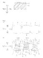
- FIG. 1 shows a cross-sectional view of a conductive adhesive sheet in an embodiment of the present invention
- FIG. 2 shows a solar cell module in an embodiment of the present invention
- FIG. 3 shows a cross-sectional view taken along line A-A of the solar cell module shown in FIG. 2 (b)
- FIG. 4 is a process drawing illustrating a method for producing a solar cell module shown in FIG. 3 .
- the directions of the conductive adhesive sheet 1 and the solar cell module 6 are based on the arrows showing directions in FIG. 1 to FIG. 4 .
- lead-free solder particles 14, high melting point metal particles 11, and a resin 15 are omitted to clearly show relative positions of the light reflective layer 3 and the conductive adhesive layer 2.
- the conductive adhesive sheet 1 is formed into an elongated sheet extending in the front-back directions, and includes a conductive adhesive layer 2, and a light reflective layer 3 formed on the surface (one surface in the thickness direction) of the conductive adhesive layer 2.
- the conductive adhesive layer 2 is formed from a conductive adhesive composition.
- the conductive adhesive composition contains, for example, lead-free solder particles, high melting point metal particles, and a resin.
- the lead-free solder that forms the lead-free solder particles is a solder that does not contain lead, and examples thereof include low melting point metal alloys such as a tin-bismuth alloy (Sn-Bi) and a tin-silver-copper alloy (Sn-Ag-Cu).
- a tin-bismuth alloy is used.
- the amount of tin in the tin-bismuth alloy is, for example, 10 to 50 mass%, preferably 25 to 45 mass%, and the amount of bismuth is, for example, 50 to 90 mass%, preferably 55 to 75 mass%.
- the lead-free solder has a melting point of, for example, 200°C or less, and for example, 140°C or more.
- the form of the lead-free solder particles is not particularly limited, and for example, the lead-free solder particles is spherical, plate-like, or needle-like. Preferably, spherical lead-free solder particles are used.
- the lead-free solder particles have an average maximum length of (when spherical, the average particle size), for example, 10 to 50 ⁇ m, preferably 20 to 40 ⁇ m.
- the lead-free solder particles When the lead-free solder particles have an average maximum length below the above-described range, the lead-free solder particles are easily oxidized, and melting (described later, ref: FIG. 4 (c) ) of the lead-free solder particles at a desired temperature (to be specific, 200°C or less) may become difficult.
- the lead-free solder particles have an average maximum length of more than the above-described range, forming of the conductive adhesive sheet 1 into a thin sheet may become difficult.
- the average maximum length is measured by using a laser diffraction/scattering particle size distribution analyzer.
- the average maximum lengths of the high melting point metal particles and the reflective particles to be described later are also measured by such a method.
- the lead-free solder particles can be used singly or in a combination of two or more.
- Examples of the high melting point metal that forms the high melting point metal particles include silver, copper, gold, platinum, titanium, zinc, aluminum, iron, nickel, and alloys thereof. Preferably, copper is used.
- the high melting point metal has a melting point of, for example, 300°C or more, preferably 400°C or more.
- the high melting point metal particles have an average maximum length (when spherical, average particle size) of, for example, 10 to 50 ⁇ m, preferably 20 to 40 ⁇ m.
- average maximum length when the high melting point metal particles have an average maximum length below the above-described range, densely filling with the high melting point metal particles may become difficult.
- the high melting point metal particles when the high melting point metal particles have an average maximum length of more than the above-described range, forming of the conductive adhesive sheet 1 into a thin sheet may become difficult.
- the high melting point metal particles can be used singly or in a combination of two or more.
- Examples of the resin include a thermosetting resin.
- thermosetting resin examples include epoxy resin, thermosetting polyimide, phenol resin, urea resin, melamine resin, diallyl phthalate resin, silicone resin, and thermosetting urethane resin.
- thermosetting resin preferably, epoxy resin, phenol resin, or thermosetting polyurethane resin is used, and more preferably, epoxy resin, or phenol resin is used.
- the epoxy resin examples include aromatic epoxy resins such as bisphenol epoxy resin (e.g., bisphenol A epoxy resin, bisphenol F epoxy resin, bisphenol S epoxy resin, hydrogenated bisphenol A epoxy resin, dimer-acid-modified bisphenol epoxy resin, etc.), novolak epoxy resin (eg., phenol novolak epoxy resin, cresol novolak epoxy resin, biphenyl epoxy resin, etc.), naphthalene epoxy resin, fluorene epoxy resin (e.g., bisarylfluorene epoxy resin, etc.), and triphenylmethane epoxy resin (e.g., trishydroxyphenylmethane epoxy resin, etc.); nitrogen-containing-cyclic epoxy resins such as triepoxypropylisocyanurate (triglycidylisocyanurate), and hydantoin epoxy resin; aliphatic epoxy resin; alicyclic epoxy resin (e.g., dicyclo ring-type epoxy resin, etc.); glycidylether epoxy resin; and
- epoxy resin preferably aromatic epoxy resin, more preferably bisphenol epoxy resin, and particularly preferably bisphenol F epoxy resin is used.
- epoxy resin a commercially available product may be used, to be specific, YSLV-80XY (bisphenol F epoxy resin, manufactured by Nippon Steel Chemical Co., Ltd.) is used.
- phenol resin examples include novolak phenol resin obtained by allowing phenol and formaldehyde to condensate in the presence of an acidic catalyst; and phenol-aralkyl resin synthesized from phenol and dimethoxyparaxylene or bis(methoxymethyl) biphenyl.
- phenol-aralkyl resin is used.
- phenol-aralkyl resin a commercially available product can be used.
- MEH-7851-SS and MEHC-7800H both manufactured by MEIWA PLASTIC INDUSTRIES, LTD. are used.
- thermosetting resin can also be prepared as a resin composition containing a thermosetting resin and a curing agent by using a curing agent in combination.
- the curing agent examples include organic phosphine compounds, imidazole compounds, amine compounds, acid anhydride compounds, amide compounds, hydrazide compounds, imidazoline compounds, and urea compounds.
- organic phosphine compounds are used.
- organic phosphine compound examples include tetraphenylphosphoniumtetraphenylborate, tetraphenylphosphoniumtetra-p-toluylborate, and tetraphenylphosphoniumtriphenylborate.
- TPP-K tetraphenylphosphoniumtetraphenylborate, manufactured by HOKKO CHEMICAL INDUSTRY CO., LTD.
- the amount of the curing agent relative to 100 parts by mass of the thermosetting resin is, for example, 0.01 to 5 parts by mass, preferably 0.05 to 1 part by mass.
- thermoplastic resins examples include thermoplastic resins.
- thermoplastic resin examples include polyolefin (e.g., polyethylene, polypropylene, ethylene-propylene copolymer, etc.), acrylic resin, polyester resin, polyvinyl acetate, an ethylene-vinyl acetate copolymer, polyvinyl chloride, polystyrene, polyacrylonitrile, polyamide (nylon (registered trademark)), polycarbonate, polyacetal, polyethylene terephthalate, polyphenylene oxide, polyphenylene sulfide, polysulfone, polyether sulfone, poly ether ether ketone, polyarylsulfone, thermoplasticpolyimide, thermoplastic urethane resin, polyaminobismaleimide, polyamideimide, polyetherimide, bismaleimidetriazine resin, polymethylpentene, fluorinated resin, liquid crystal polymer, an olefin-vinyl alcohol copolymer, ionomer, polyarylate, acrylonit
- thermoplastic resin preferably, acrylic resin, and polyester resin are used, and more preferably, acrylic resin is used.
- the acrylic resin is composed of an acrylic polymer, and examples of such an acrylic polymer include a polymer of a monomer containing alkyl (meth) acrylate having 1 to 12 carbon atoms in its alkyl moiety as a main component, including methyl (meth) acrylate, ethyl (meth) acrylate, propyl (meth) acrylate, butyl (meth) acrylate, hexyl (meth) acrylate, octyl (meth) acrylate, decyl (meth) acrylate, and dodecyl (meth) acrylate.
- acrylic polymer a commercially available product can be used.
- LA polymer manufactured by Kuraray Co., Ltd.
- SG-700AS manufactured by Nagase ChemteX Corporation
- UC-3510 manufactured by TOAGOSEI CO., LTD.
- thermosetting resin and a thermoplastic resin are used in combination, or a thermosetting resin is used alone.
- thermosetting resin As an example of a combination of a thermosetting resin and a thermoplastic resin, to be specific, a combination of epoxy resin and phenol resin as thermosetting resins, and acrylic resin as a thermoplastic resin may be used.
- the amount of the thermosetting resin relative to the resin is, for example, 10 to 90 mass%, preferably 20 to 80 mass%.
- the epoxy resin is used in an amount of, relative to the thermosetting resin, for example, 10 to 90 mass%, preferably 20 to 80 mass%; and phenol resin is used in an amount of, relative to the thermosetting resin, for example, 10 to 90 mass%, preferably 20 to 80 mass%.
- the amount of the thermoplastic resin used in combination with the thermosetting resin relative to 100 parts by mass of the thermosetting resin is, for example, 10 to 90 parts by mass, preferably 20 to 80 parts by mass.
- the resin can also be prepared as a resin composition containing a resin and an activator.
- the activator is optionally blended to the resin composition to melt the lead-free solder particles easily.
- activator examples include organic carboxylic acids such as adipic acid, sebacic acid, 2-phenoxybenzoic acid.
- the amount of the activator relative to the total amount of the lead-free solder particles and the high melting point metal particles is, for example, 0.1 to 20 mass%, preferably 0.5 to 5 mass%.
- the proportion of the total amount in volume of the lead-free solder particles and the high melting point metal particles relative to the conductive adhesive composition is, for example, 50 to 90 vol%, preferably 60 to 85 vol%.
- the proportion of the above-described the total volume amount is more than the above-described range, the lead-free solder particles and the high melting point metal particles may not be blended into the conductive adhesive composition.
- the above-described total volume amount is below the above-described range, electrical connection may not be obtained.
- the ratio of the lead-free solder particles relative to the high melting point metal particles is, on the basis of volume, for example, 0.25 to 4, preferably 0.4 to 2.5.
- the ratio is more than the above-described range, costs may increase.
- the ratio is below the above-described lower limit, conductive path (described later, ref: FIG. 4 (c) ) between the high melting point metal particles may not be obtained.
- the conductive adhesive composition is prepared by blending the lead-free solder particles, the high melting point metal particles, the resin, and as necessary, an activator in the above-described amounts.
- the above-described components are kneaded by a kneader, so as to prepare the conductive adhesive composition as a kneaded material.
- the prepared kneaded material is molded into a sheet, thereby producing a conductive adhesive layer 2.
- the conductive adhesive layer 2 is molded into a sheet, for example, by extrusion molding using a T-die.
- the conductive adhesive layer 2 has a thickness of, for example, 10 to 200 ⁇ m, preferably 50 to 100 ⁇ m.
- the thickness of the conductive adhesive layer 2 is more than the above-described range, costs may increase.
- the thickness of the conductive adhesive layer 2 is below the above-described range, the thickness may become smaller than the average maximum length of the lead-free solder particles and/or the high melting point metal particles, and in such a case, molding into a sheet may be difficult.
- the light reflective layer 3 is laminated on the entire top surface of the conductive adhesive layer 2.
- the light reflective layer 3 is formed from a reflective composition.
- the reflective composition contains reflective particles and a resin.
- the reflective particles are blended in the reflective composition to impart light reflectivity to the light reflective layer 3.
- the reflective particles are, for example, white particles, and examples of such white particles include, to be specific, white pigment.
- white pigment examples include white inorganic pigment, and such white inorganic pigment include, for example, oxides such as titanium oxide particles, silicon oxide (silica) particles, aluminum oxide (alumina), zinc oxide, and zirconium oxide; and carbonates such as white lead (lead carbonate), and calcium carbonate; and clay minerals such as kaolin (kaolinite).
- oxides such as titanium oxide particles, silicon oxide (silica) particles, aluminum oxide (alumina), zinc oxide, and zirconium oxide
- carbonates such as white lead (lead carbonate), and calcium carbonate
- clay minerals such as kaolin (kaolinite).
- oxide particles more preferably, titanium oxide particles are used.
- titanium oxide particles characteristics such as high whiteness, high light reflectivity, high dispersiveness, excellent weatherability, and high chemical stability can be obtained.
- Such titanium oxide particles are, to be specific, particles composed of TiO 2 (titanium oxide (IV), titanium dioxide).
- the form of the reflective particles is not particularly limited, and for example, spherical, plate-like, or needle-like.
- the reflective particles have an average maximum length of (when spherical, the average particle size), for example, 100 to 500 nm. When the average maximum length of the reflective particles is outside the above-described range, reflectance of the light reflective layer 3 for visible light (wavelength 300 to 800 nm) is reduced, and effects of sunlight reflection (described later) may not be obtained sufficiently.
- the above-described resin may be used, and preferably, a combination of a thermosetting resin and a thermoplastic resin may be used.
- thermosetting resin preferably, an aromatic epoxy resin is used, and more preferably, bisphenol epoxy resin, or novolak epoxy resin is used, and particularly preferably, bisphenol A epoxy resin, or cresol novolak epoxy resin is used.
- An example of a commercially available product of bisphenol A epoxy resin includes Epikote YL980 (manufactured by JER), and an example of a commercially available product of cresol novolak epoxy resin include KI-3000 (manufactured by JER).
- thermoplastic resin preferably, acrylic resin is used.
- Examples of a commercially available product of acrylic resin include SG-700AS (manufactured by Nagase ChemteX Corporation) and UC-3510 (manufactured by TOAGOSEI CO., LTD.).
- the amount of the thermosetting resin relative to the resin is, for example, 10 to 90 mass%, preferably 20 to 80 mass%.
- the amount of the epoxy resin relative to the thermosetting resin is, for example, 10 to 90 mass%, preferably 20 to 80 mass%.
- the amount of the thermoplastic resin relative to 100 parts by mass of the thermosetting resin is, for example, 10 to 90 parts by mass, preferably 20 to 80 parts by mass.
- the amount of the reflective particles relative to the reflective composition is, on volume basis, for example, 10 to 40 vol%, preferably 15 to 35 vol%.
- the reflectance of the light reflective layer 3 decreases. Furthermore, to prevent such a decrease in reflectance, the thickness of the light reflective layer 3 has to be made larger to that extent. Then, as shown in FIG. 4 (c) , fusion bonding (described later) of the lead-free solder particles 14 encapsulated by the light reflective layer 3 to the back electrode 4 may become difficult.
- the amount of the reflective particles is more than the above-described range, that is, when the amount of the resin is extremely small, the viscosity of the reflective composition becomes excessively high, and therefore fusion bonding (described later) of the lead-free solder particles 14 encapsulated by the light reflective layer 3 to the back electrode 4 may become difficult.
- the amount of the resin relative to the reflective composition is, on volume basis, for example, 60 to 90 vol%, preferably 65 to 85 vol%.
- the reflective composition can be prepared as a kneaded material, by blending reflective particles and a resin, and for example, by kneading the mixture with a kneader.
- the light reflective layer 3 is formed by molding the prepared kneaded material into a sheet.
- the light reflective layer 3 is molded into a sheet by extrusion molding with a T-die provided in a kneader.
- the reflectance of the light reflective layer 3 for light at a wavelength of 460 nm is, for example, 70 to 90%.
- the light reflective layer 3 has a thickness of, for example, 1 to 15 ⁇ m, preferably 5 to 12 ⁇ m. When the thickness of the light reflective layer 3 is more than the above-described range, as shown in FIG. 4 (c) , fusion bonding (described later) of the lead-free solder particles 14 encapsulated by the light reflective layer 3 to the back electrode 4 may become difficult.
- the thickness of the light reflective layer 3 is below the above-described range, the reflectance of the light reflective layer 3 decreases, and effects of sunlight reflection (described later) may not be obtained sufficiently.
- the conductive adhesive sheet 1 is obtained by, as shown in FIG. 1 , bonding the above-described conductive adhesive layer 2 and the light reflective layer 3 together.
- a solar cell module 6 including a plurality of back contact solar cells 5 having back electrodes 4 connected by a conductive adhesive sheet 1 .
- the solar cell module 6 includes, as shown in FIG. 2 (b) , a plurality of back contact solar cells 5 disposed in the front-back directions in spaced-apart relation to each other, and a conductive adhesive sheet 1 that connects the back electrodes 4 of the plurality of back contact solar cells 5.
- the back contact solar cell 5 is formed into a generally rectangular shape when viewed from the top, and the plurality of back contact solar cells 5 are arranged in line along the front-back directions.
- the top surfaces of the plurality of back contact solar cells 5 serve as a light-receiving surface that receives sunlight and generates electric energy.
- back electrodes 4 for taking out the electric energy generated at the light-receiving surface are provided at the bottom surfaces (rear surface) of the plurality of back contact solar cells 5.
- the back electrodes 4 are formed into an electrode pattern having a positive electrode 7 and a negative electrode 8.
- the positive electrode 7 is formed into a generally comb shape with opening toward a rear side.
- the positive electrode 7 integrally includes, at the front end portion of the rear surface of the back contact solar cell 5, a positive electrode-side current collecting portion 9 extending in the left-right directions, and a plurality of positive electrode-side comb tooth portions 10 extending toward the rear side from the positive electrode-side current collecting portion 9 and arranged parallely in the left-right directions in spaced-apart relation to each other.
- the negative electrode 8 is formed into a generally comb shape with opening toward the front side.
- the negative electrode 8 integrally includes, at the rear end portion of the rear surface of the back contact solar cell 5, a negative electrode-side current collecting portion 12 extending in the left-right directions, and a plurality of negative electrode-side comb tooth portions 13 extending from the negative electrode-side current collecting portion 12 toward the front side and arranged parallely in the left-right directions in spaced-apart relation to each other.
- the positive electrode-side comb tooth portion 10 and the negative electrode-side comb tooth portion 13 are alternately disposed in spaced-apart relation in the left-right directions.
- the conductive adhesive sheet 1 connects, as shown in FIG. 2 (b) and FIG. 3 , the back electrodes 4 of the back contact solar cells 5 that are adjacent to each other in front-back directions.
- the conductive adhesive sheet 1 allows connection between the positive electrode 7 of the first back contact solar cell 5A and the negative electrode 8 of the second back contact solar cell 5B that is disposed adjacently in front of the first back contact solar cell 5A.
- the conductive adhesive sheet 1 allows connection between the positive electrode 7 and the negative electrode 8 so as to extend over the positive electrode-side current collecting portion 9 of the first back contact solar cell 5A and the negative electrode-side current collecting portion 12 of the second back contact solar cell 5B.
- the top surface of the both end portions in the front-back directions of the light reflective layer 3 are in contact with the edge portion (inner side portion) of the positive electrode-side current collecting portion 9 of the first back contact solar cell 5A, and with edge portion (inner side portion) of the negative electrode-side current collecting portion 12 of the second back contact solar cell 5B.
- the light reflective layer 3 is not formed at a portion facing the back electrode 4, and the surface of the conductive adhesive layer 2 not overlapping the light reflective layer 3 is directly in contact with the back electrode 4.
- the conductive adhesive layer 2 at both end portions in the front-back directions is allowed to directly contact with the positive electrode-side current collecting portion 9 of the first back contact solar cell 5A and the negative electrode-side current collecting portion 12 of the second back contact solar cell 58.
- the light reflective layer 3 at the middle portion of the conductive adhesive sheet 1 in the front-back directions is exposed from the gaps between the plurality of back contact solar cells 5 to the upper side, and is allowed to directly contact with the bottom surface and the side surface of the end portions of the first back contact solar cell 5A and the second back contact solar cell 5B at the side where they are facing each other (inner side).
- a plurality of back contact solar cells 5 are prepared, and these are arranged in line in the front-back directions.
- the conductive adhesive sheet 1 is placed on the rear surface of the back contact solar cell 5 so as to extend over the positive electrode-side current collecting portion 9 and the negative electrode-side current collecting portion 12 of the adjacent back contact solar cells 5.
- the conductive adhesive sheet 1 is allowed to adhere to the back electrodes 4 (the positive electrode 7 and the negative electrode 8).
- thermocompression bonding step To allow the conductive adhesive sheet 1 to adhere to the back electrodes 4, as shown in FIG. 4 (b) , the conductive adhesive sheet I and the back electrodes 4 are thermocompression bonded (first thermocompression bonding step).
- the temperature in the first thermocompression bonding step is, for example, 80°C or more and below 140°C, preferably 100°C or more and 130°C or less, and the pressure is, for example, 0.1 to 2MPa, preferably 0.2 to 1MPa.
- the conductive adhesive sheet 1 softens.
- thermosetting resin when the conductive adhesive composition contains a thermosetting resin, the thermosetting resin is brought into B-stage state (semi-cured state). Furthermore, when the conductive adhesive layer 2 contains a thermoplastic resin, the thermosetting resin softens.
- thermosetting resin when the reflective composition contains a thermosetting resin, the thermosetting resin is brought into B-stage state (semi-cured state). Furthermore, when the conductive adhesive layer 2 contains a thermoplastic resin, the thermosetting resin softens.
- the light reflective layer 3 facing the back electrodes 4 moves downwardly, and enters into the B-staged and/or softened conductive adhesive layer 2.
- the light reflective layer 3 (widthwise center) that does not face the back electrode 4 in the thickness direction relatively moves upwardly relative to the light reflective layer 3 (widthwise both end portions) that faces the back electrode 4.
- the widthwise both end portions of the light reflective layer 3 that entered into the conductive adhesive layer 2 encapsulate (embeds) the lead-free solder particles 14.
- the lead-free solder particles 14 that are encapsulated in the light reflective layer 3 are in contact with the back electrode 4, or present in the proximity of the back electrode 4.
- thermocompression bonding step Thereafter, as shown in FIG. 4 (c) , the conductive adhesive sheet 1 and the back electrodes 4 are further thermocompression bonded (second thermocompression bonding step).
- the temperature is, for example, 140°C or more, and 200°C or less
- the pressure is, for example, 0.1 to 2MPa, preferably 0.2 to 1MPa.
- the lead-free solder particles 14 cover the high melting point metal particles 11 that are adjacent to each other, and are formed to be continuous, extending over the high melting point metal particles 11.
- a conductive path 20 composed of a lead-free solder that forms the lead-free solder particles 14 is formed in the conductive adhesive layer 2.
- the lead-free solder particles 14 that are facing the back electrode 4 fusion bond (weld) the bottom surface of the back electrodes 4.
- the conductive path 20 that electrically connects (allows electrical continuity) the positive electrode 7 and the negative electrode 8 is formed.
- thermosetting resin is brought into C stage state (completely cured).
- the reflective composition contains a thermoplastic resin
- the thermosetting resin melts, and therefore the reflective particles are diffused in the conductive adhesive layer 2.
- the light reflective layer 3 that faces the back contact solar cell 5 substantially disappears.
- the conductive adhesive sheet 1 is allowed to adhere to the back electrodes 4 (the positive electrode 7 and the negative electrode 8) of the back contact solar cell 5.
- the conductive adhesive sheet 1 connects the back electrodes 4 of the plurality of back contact solar cells 5 disposed in spaced-apart relation to each other.
- the plurality of back contact solar cells 5 are bonded and fixed, electrical conduction between the back electrodes 4 is achieved.
- the conductive adhesive layer 2 and the light reflective layer 3 allow reinforcement around the solder joining portion between the conductive adhesive sheet 1, and the back electrodes 4 joined by the conductive adhesive sheet 1.
- the resin reinforces the above-described portion for sure.
- the rear surface of the conductive adhesive layer 2 is exposed.
- a metal foil 16 can be provided on the rear surface of the conductive adhesive layer 2.
- the metal foil 16 is laminated on the entire rear surface of the conductive adhesive layer 2.
- metals that form the metal foil 16 include copper, silver, and gold. Preferably, copper is used.
- the metal foil 16 has a thickness of, for example, 18 to 150 ⁇ m, preferably 30 to 75 ⁇ m.
- the metal foil 16 supports the conductive adhesive layer 2 to further improve the mechanical strength of the solar cell module 6.
- a resin composition was prepared as a kneaded material by blending 32 parts by mass of epoxy resin (YSLV-80XY, bisphenol F epoxy resin, manufactured by Nippon Steel Chemical Co., Ltd.); 33 parts by mass of phenol resin (MEH-7851-SS, phenol-aralkyl resin, manufactured by MEIWA PLASTIC INDUSTRIES, LTD.); 30 parts by mass of acrylic resin (LA polymer, acrylic polymer, manufactured by Kuraray Co., Ltd.); and 5 parts by mass of active agent (2-phenoxybenzoic acid).
- epoxy resin YSLV-80XY, bisphenol F epoxy resin, manufactured by Nippon Steel Chemical Co., Ltd.
- MEH-7851-SS phenol-aralkyl resin, manufactured by MEIWA PLASTIC INDUSTRIES, LTD.
- acrylic resin LA polymer, acrylic polymer, manufactured by Kuraray Co., Ltd.
- active agent (2-phenoxybenzoic acid 2-phenoxybenzoic acid
- the resin composition lead-free solder particles (42Sn-58Bi, copper-bismuth alloy particles, melting point 139°C, spherical, average particle size 35 ⁇ m), and copper particles (melting point 1083°C, spherical, average particle size 20 ⁇ m) were kneaded so that their volume ratio was 30: 20: 50, thereby preparing a conductive adhesive composition as a kneaded material.
- lead-free solder particles 42Sn-58Bi, copper-bismuth alloy particles, melting point 139°C, spherical, average particle size 35 ⁇ m
- copper particles melting point 1083°C, spherical, average particle size 20 ⁇ m
- the kneaded material was molded into a 50 ⁇ m sheet, thereby producing a conductive adhesive layer.
- a varnish was prepared by blending the following in 41 parts by mass of methyl ethyl ketone: 41 parts by mass of acrylic resin A (SG-700AS, acrylic polymer, manufactured by Nagase ChemteX Corporation); 1.7 parts by mass of acrylic resin B (UC-3510, acrylic polymer, manufactured by TOAGOSEI CO., LTD.); 7.9 parts by mass of epoxy resin A (KI-3000, cresol novolak epoxy resin, manufactured by JER); 21 parts by mass of epoxy resin B (EpikoteYL980, bisphenol A epoxy resin, manufactured by JER); 28 parts by mass of phenol resin (MEHC-7800H, phenol-aralkyl resin, manufactured by MEIWA PLASTIC INDUSTRIES.LTD.); and 0.068 parts by mass of a curing agent (TPP-K, tetraphenylphosphoniumtetraphenylborate, manufactured by HOKKO CHEMICAL INDUSTRY CO., LTD.).
- acrylic resin A SG-700AS, acrylic
- the varnish and titanium oxide particles (spherical, average particle size 250 nm) were mixed so that their volume ratio was 82: 18 (solid content: titanium oxide particles), and the mixture was kneaded so that their volume ratio was 30: 20: 50, thereby preparing a reflective composition as a kneaded material.
- the kneaded material was molded into a 10 ⁇ m sheet, thereby producing a light reflective layer.
- the conductive adhesive layer and the light reflective layer were bonded together, thereby producing a conductive adhesive sheet (ref: FIG. 1 ).
- a conductive adhesive layer was made in the same manner as in Example 1, except that the resin composition, the lead-free solder particles, and the copper particles were kneaded so that the volume ratio between them was 30: 35: 35 in the preparation of a conductive adhesive layer; and then a conductive adhesive sheet was made.
- a conductive adhesive layer was made in the same manner as in Example I , except that the resin composition, the lead-free solder particles, and the copper particles were kneaded so that the volume ratio between them was 30: 50: 20 in the preparation of a conductive adhesive layer; and then a conductive adhesive sheet was made.
- a conductive adhesive layer was made in the same manner as in Example 1, except that in the preparation of the conductive adhesive layer, lead-free solder particles (Sn-Ag-Cu, 96.5: 3: 0.5 mass ratio, melting point 220°C, spherical, average particle size 35 ⁇ m) were blended instead of the lead-free solder particles (42Sn-58Bi); and then a conductive adhesive sheet was made.
- lead-free solder particles Sn-Ag-Cu, 96.5: 3: 0.5 mass ratio, melting point 220°C, spherical, average particle size 35 ⁇ m
- a conductive adhesive layer was made in the same manner as in Example 1, except that the resin composition, the lead-free solder particles, and the copper particles were kneaded so that the volume ratio between them was 30: 10: 60 in the preparation of a conductive adhesive layer; and then a conductive adhesive sheet was made.
- a resin layer composed of acrylic resins A and B, a phenol resin, epoxy resins A and B, and a curing agent was made in the same manner as in Example 1, except that titanium oxide particles were not blended in the production of the light reflective layer; and then a conductive adhesive sheet was made.
- Adhesiveness of the conductive adhesive sheets was evaluated by allowing the conductive adhesive sheet of Examples and Comparative Examples to adhere to copper foil with its front surface and rear surface covered (plated) with tin, and conducting their continuity test.
- thermocompression bonding step ref: FIG. 4 (b) ).
- the conductive adhesive sheet was softened in this manner.
- thermocompression bonding step ref: FIG. 4 (c) ).
- the conductive adhesive sheet was allowed to adhere to the copper foil in this manner.
- the surfaces of the copper particles were covered with the lead-free solder particles, and the light reflective layer disappeared.
- a conductive path electrically connecting with the copper foil was formed in the conductive adhesive layer.
- the reflectance of the conductive adhesive sheets of Examples and Comparative Examples for light at a wavelength of 460 nm was measured with a spectrometer for evaluation.
- the light reflectivity of the conductive adhesive sheet was evaluated based on the following evaluation criteria.
- the reflectance of the conductive adhesive sheet was 70% or more.
Landscapes
- Chemical & Material Sciences (AREA)
- Organic Chemistry (AREA)
- Inorganic Chemistry (AREA)
- Photovoltaic Devices (AREA)
- Conductive Materials (AREA)
- Non-Insulated Conductors (AREA)
Applications Claiming Priority (1)
| Application Number | Priority Date | Filing Date | Title |
|---|---|---|---|
| JP2012002070A JP2013143426A (ja) | 2012-01-10 | 2012-01-10 | 導電性接着シートおよび太陽電池モジュール |
Publications (1)
| Publication Number | Publication Date |
|---|---|
| EP2615146A2 true EP2615146A2 (fr) | 2013-07-17 |
Family
ID=47563187
Family Applications (1)
| Application Number | Title | Priority Date | Filing Date |
|---|---|---|---|
| EP13150469.8A Withdrawn EP2615146A2 (fr) | 2012-01-10 | 2013-01-08 | Élément adhésif conducteur et module de cellule solaire |
Country Status (6)
| Country | Link |
|---|---|
| US (1) | US20130174886A1 (fr) |
| EP (1) | EP2615146A2 (fr) |
| JP (1) | JP2013143426A (fr) |
| KR (1) | KR20130082109A (fr) |
| CN (1) | CN103199122A (fr) |
| TW (1) | TW201329192A (fr) |
Cited By (4)
| Publication number | Priority date | Publication date | Assignee | Title |
|---|---|---|---|---|
| EP2869349A3 (fr) * | 2013-10-29 | 2015-05-27 | Lg Electronics Inc. | Cellule solaire et module de cellule solaire |
| EP2879188A1 (fr) * | 2013-11-29 | 2015-06-03 | LG Electronics Inc. | Cellule solaire et son procédé de fabrication |
| EP2911206A3 (fr) * | 2014-02-24 | 2015-11-25 | LG Electronics Inc. | Module de cellule solaire et son procédé de fabrication |
| WO2016086466A1 (fr) * | 2014-12-04 | 2016-06-09 | 友达光电股份有限公司 | Module solaire comprenant un ruban adhésif |
Families Citing this family (11)
| Publication number | Priority date | Publication date | Assignee | Title |
|---|---|---|---|---|
| JP6092754B2 (ja) * | 2013-11-12 | 2017-03-08 | 信越化学工業株式会社 | 導電性エポキシ樹脂組成物、該組成物を用いた太陽電池セル、及び該太陽電池セルの製造方法 |
| CN103943704A (zh) * | 2014-03-18 | 2014-07-23 | 连云港神舟新能源有限公司 | 一种指叉背接触太阳电池组件及其制备方法 |
| KR102271055B1 (ko) * | 2014-06-26 | 2021-07-01 | 엘지전자 주식회사 | 태양 전지 모듈 |
| US20160163901A1 (en) * | 2014-12-08 | 2016-06-09 | Benjamin Ian Hsia | Laser stop layer for foil-based metallization of solar cells |
| JP6624418B2 (ja) * | 2015-03-13 | 2019-12-25 | パナソニックIpマネジメント株式会社 | 太陽電池モジュール |
| JP6310954B2 (ja) * | 2015-05-29 | 2018-04-11 | 株式会社タムラ製作所 | 導電性接着剤および電子基板の製造方法 |
| JP6710120B2 (ja) * | 2015-09-30 | 2020-06-17 | 太陽インキ製造株式会社 | 導電性接着剤、電子部品および電子部品の製造方法 |
| JP6830201B2 (ja) * | 2016-03-29 | 2021-02-17 | パナソニックIpマネジメント株式会社 | 太陽電池モジュールの製造方法 |
| CN106449823A (zh) * | 2016-11-30 | 2017-02-22 | 庞倩桃 | 双玻光伏组件 |
| US10640232B2 (en) * | 2016-12-20 | 2020-05-05 | The Boeing Company | Conductive fastening system for composite structures |
| CN111403118B (zh) * | 2018-12-27 | 2021-09-07 | 广西纵览线缆集团有限公司 | 抗拉耐热铝合金导线的制造工艺 |
Citations (1)
| Publication number | Priority date | Publication date | Assignee | Title |
|---|---|---|---|---|
| JP2011159726A (ja) | 2010-01-29 | 2011-08-18 | Toppan Printing Co Ltd | 太陽電池モジュールの製造方法 |
Family Cites Families (21)
| Publication number | Priority date | Publication date | Assignee | Title |
|---|---|---|---|---|
| US4232070A (en) * | 1978-11-07 | 1980-11-04 | Trw Inc. | Non-arcing dielectric modular array |
| JPH0697573B2 (ja) * | 1984-09-18 | 1994-11-30 | 日立化成工業株式会社 | 回路の接続部材 |
| JPH065116A (ja) * | 1992-06-19 | 1994-01-14 | Shin Etsu Polymer Co Ltd | 低融点金属接合型異方導電膜 |
| US5428249A (en) * | 1992-07-15 | 1995-06-27 | Canon Kabushiki Kaisha | Photovoltaic device with improved collector electrode |
| JP2939075B2 (ja) * | 1992-12-24 | 1999-08-25 | キヤノン株式会社 | 太陽電池モジュール |
| JP3493101B2 (ja) * | 1996-08-15 | 2004-02-03 | 三井金属鉱業株式会社 | 半田粉及びその製造方法、及びその半田粉を用いた半田ペースト |
| US6008449A (en) * | 1997-08-19 | 1999-12-28 | Cole; Eric D. | Reflective concentrating solar cell assembly |
| JP2006199937A (ja) * | 2004-12-15 | 2006-08-03 | Tamura Kaken Co Ltd | 導電性接着剤、これを用いた導電部及び電子部品モジュール |
| US20090293934A1 (en) * | 2005-11-10 | 2009-12-03 | Kyocera Corporation | Photoelectric Conversion Device |
| CN102942883B (zh) * | 2006-04-26 | 2015-08-26 | 日立化成株式会社 | 粘接带及使用其的太阳能电池模块 |
| US20100155964A1 (en) * | 2006-04-27 | 2010-06-24 | Sumitomo Bakelite Co., Ltd. | Adhesive Tape, Semiconductor Package and Electronics |
| JP5121181B2 (ja) * | 2006-07-28 | 2013-01-16 | 三洋電機株式会社 | 光起電力素子及びその製造方法 |
| EP2109894A2 (fr) * | 2007-01-31 | 2009-10-21 | Renewable Energy Corporation ASA | Ruban d'interconnexion réfléchissant pour modules solaires |
| US20090032087A1 (en) * | 2007-02-06 | 2009-02-05 | Kalejs Juris P | Manufacturing processes for light concentrating solar module |
| JP4989549B2 (ja) * | 2007-08-24 | 2012-08-01 | 三洋電機株式会社 | 太陽電池及び太陽電池モジュール |
| US20090050190A1 (en) * | 2007-08-24 | 2009-02-26 | Sanyo Electric Co., Ltd. | Solar cell and solar cell module |
| JP5317712B2 (ja) * | 2008-01-22 | 2013-10-16 | 株式会社半導体エネルギー研究所 | 半導体装置及び半導体装置の作製方法 |
| KR20110008284A (ko) * | 2008-04-29 | 2011-01-26 | 어플라이드 머티어리얼스, 인코포레이티드 | 모놀리식 모듈 어셈블리 기술들을 이용하여 제조된 광전지 모듈들 |
| US20100206352A1 (en) * | 2009-02-13 | 2010-08-19 | Applied Materials, Inc. | Low-concentration flat profile photovoltaic modules |
| JP5402109B2 (ja) * | 2009-02-27 | 2014-01-29 | デクセリアルズ株式会社 | 異方性導電フィルム及び発光装置 |
| PH12012500718A1 (en) * | 2009-10-15 | 2012-10-29 | Hitachi Chemical Co Ltd | Conductive adhesive, solar cell, method for manufacturing solar cell, and solar cell module |
-
2012
- 2012-01-10 JP JP2012002070A patent/JP2013143426A/ja not_active Ceased
- 2012-12-28 TW TW101150974A patent/TW201329192A/zh unknown
-
2013
- 2013-01-08 EP EP13150469.8A patent/EP2615146A2/fr not_active Withdrawn
- 2013-01-09 US US13/737,259 patent/US20130174886A1/en not_active Abandoned
- 2013-01-09 KR KR1020130002419A patent/KR20130082109A/ko not_active Withdrawn
- 2013-01-10 CN CN2013100098838A patent/CN103199122A/zh active Pending
Patent Citations (1)
| Publication number | Priority date | Publication date | Assignee | Title |
|---|---|---|---|---|
| JP2011159726A (ja) | 2010-01-29 | 2011-08-18 | Toppan Printing Co Ltd | 太陽電池モジュールの製造方法 |
Cited By (10)
| Publication number | Priority date | Publication date | Assignee | Title |
|---|---|---|---|---|
| EP2869349A3 (fr) * | 2013-10-29 | 2015-05-27 | Lg Electronics Inc. | Cellule solaire et module de cellule solaire |
| US9871149B2 (en) | 2013-10-29 | 2018-01-16 | Lg Electronics Inc. | Solar cell and solar cell module |
| EP2879188A1 (fr) * | 2013-11-29 | 2015-06-03 | LG Electronics Inc. | Cellule solaire et son procédé de fabrication |
| US10170647B2 (en) | 2013-11-29 | 2019-01-01 | Lg Electronics Inc. | Solar cell and method for manufacturing the same |
| EP2911206A3 (fr) * | 2014-02-24 | 2015-11-25 | LG Electronics Inc. | Module de cellule solaire et son procédé de fabrication |
| US9553226B2 (en) | 2014-02-24 | 2017-01-24 | Lg Electronics Inc. | Solar cell module and method for manufacturing the same |
| US10475944B2 (en) | 2014-02-24 | 2019-11-12 | Lg Electronics Inc. | Solar cell module and method for manufacturing the same |
| US11538952B2 (en) | 2014-02-24 | 2022-12-27 | Shangrao Jinko Solar Technology Development Co., Ltd. | Solar cell module and method for manufacturing the same |
| WO2016086466A1 (fr) * | 2014-12-04 | 2016-06-09 | 友达光电股份有限公司 | Module solaire comprenant un ruban adhésif |
| DE112014007230B4 (de) * | 2014-12-04 | 2020-12-10 | Au Optronics Corporation | Klebeband und dessen verwendung für ein solarmodul |
Also Published As
| Publication number | Publication date |
|---|---|
| JP2013143426A (ja) | 2013-07-22 |
| CN103199122A (zh) | 2013-07-10 |
| KR20130082109A (ko) | 2013-07-18 |
| TW201329192A (zh) | 2013-07-16 |
| US20130174886A1 (en) | 2013-07-11 |
Similar Documents
| Publication | Publication Date | Title |
|---|---|---|
| EP2615146A2 (fr) | Élément adhésif conducteur et module de cellule solaire | |
| EP2645827B1 (fr) | Feuille de jonction, composant électronique et procédé de production associé | |
| KR102159992B1 (ko) | 이방성 도전 접착제 | |
| KR102568476B1 (ko) | 접속체의 제조 방법, 이방성 접합 필름, 접속체 | |
| EP2654389B1 (fr) | Feuille de jonction, composant électronique et procédé de fabrication associé | |
| KR102190150B1 (ko) | 도전성 접착 필름 및 이를 이용한 다이싱·다이본딩 필름 | |
| EP2086018A1 (fr) | Procede de connexion de cellules de batterie solaire et module batterie solaire | |
| KR101254474B1 (ko) | 회로 접속 재료 및 접속 구조체 | |
| EP2899244A1 (fr) | Adhésif conducteur anisotrope et structure de jonction | |
| EP3675180B1 (fr) | Module de cellule solaire incluant des cellules solaires | |
| JP2012009706A (ja) | 太陽電池モジュール及びその製造方法 | |
| KR20120007008A (ko) | 태양전지 모듈 및 그 제조 방법 | |
| TW201447922A (zh) | 光反射性導電粒子、異向性導電接著劑及發光裝置 | |
| JP2009283606A (ja) | 配線部材の接続構造体及び配線部材の接続方法 | |
| US10412838B2 (en) | Conductive particle, and connection material, connection structure, and connecting method of circuit member | |
| TWI568005B (zh) | A solar cell module manufacturing method, a solar cell conductive adhesive agent, a solar cell module | |
| JP2012009753A (ja) | 太陽電池モジュール用導電材料及び太陽電池モジュール | |
| US20250219004A1 (en) | Connecting structure | |
| CN1783471A (zh) | 半导体封装及半导体模块 | |
| CN213960387U (zh) | 一种耐候性能好的线路板 | |
| CN105324854A (zh) | 背接触式的太阳能电池模块的制造方法 | |
| KR20240135250A (ko) | 도전성 필름의 접합체 및 이의 제조방법 | |
| JP2012216294A (ja) | 複合粒子、樹脂組成物及び接続構造体 | |
| JP2016195201A (ja) | 導電性接着ペースト、並びに太陽電池モジュール及びその製造方法 | |
| JP2014225443A (ja) | 導電性粒子、導電性粒子の製造方法、導電材料及び接続構造体 |
Legal Events
| Date | Code | Title | Description |
|---|---|---|---|
| PUAI | Public reference made under article 153(3) epc to a published international application that has entered the european phase |
Free format text: ORIGINAL CODE: 0009012 |
|
| AK | Designated contracting states |
Kind code of ref document: A2 Designated state(s): AL AT BE BG CH CY CZ DE DK EE ES FI FR GB GR HR HU IE IS IT LI LT LU LV MC MK MT NL NO PL PT RO RS SE SI SK SM TR |
|
| AX | Request for extension of the european patent |
Extension state: BA ME |
|
| STAA | Information on the status of an ep patent application or granted ep patent |
Free format text: STATUS: THE APPLICATION HAS BEEN WITHDRAWN |
|
| 18W | Application withdrawn |
Effective date: 20151027 |