EP2620747A2 - Vibrator und Vibrationskreisel - Google Patents
Vibrator und Vibrationskreisel Download PDFInfo
- Publication number
- EP2620747A2 EP2620747A2 EP13165482.4A EP13165482A EP2620747A2 EP 2620747 A2 EP2620747 A2 EP 2620747A2 EP 13165482 A EP13165482 A EP 13165482A EP 2620747 A2 EP2620747 A2 EP 2620747A2
- Authority
- EP
- European Patent Office
- Prior art keywords
- vibration piece
- vibrator
- driving
- detection
- thickness
- Prior art date
- Legal status (The legal status is an assumption and is not a legal conclusion. Google has not performed a legal analysis and makes no representation as to the accuracy of the status listed.)
- Granted
Links
- 238000001514 detection method Methods 0.000 claims abstract description 52
- 238000005452 bending Methods 0.000 claims abstract description 18
- 238000005530 etching Methods 0.000 claims description 8
- 239000013078 crystal Substances 0.000 claims description 7
- 239000010453 quartz Substances 0.000 claims description 5
- VYPSYNLAJGMNEJ-UHFFFAOYSA-N silicon dioxide Inorganic materials O=[Si]=O VYPSYNLAJGMNEJ-UHFFFAOYSA-N 0.000 claims description 5
- 238000002474 experimental method Methods 0.000 description 10
- VYZAMTAEIAYCRO-UHFFFAOYSA-N Chromium Chemical compound [Cr] VYZAMTAEIAYCRO-UHFFFAOYSA-N 0.000 description 9
- 229910052804 chromium Inorganic materials 0.000 description 9
- 239000011651 chromium Substances 0.000 description 9
- PCHJSUWPFVWCPO-UHFFFAOYSA-N gold Chemical compound [Au] PCHJSUWPFVWCPO-UHFFFAOYSA-N 0.000 description 9
- 239000010931 gold Substances 0.000 description 9
- 229910052737 gold Inorganic materials 0.000 description 9
- 239000000758 substrate Substances 0.000 description 8
- 239000007864 aqueous solution Substances 0.000 description 7
- 238000006073 displacement reaction Methods 0.000 description 7
- 238000005259 measurement Methods 0.000 description 6
- 238000000034 method Methods 0.000 description 6
- VLTRZXGMWDSKGL-UHFFFAOYSA-N perchloric acid Chemical compound OCl(=O)(=O)=O VLTRZXGMWDSKGL-UHFFFAOYSA-N 0.000 description 6
- 230000035945 sensitivity Effects 0.000 description 6
- 238000010586 diagram Methods 0.000 description 5
- 229920002120 photoresistant polymer Polymers 0.000 description 5
- 230000008859 change Effects 0.000 description 4
- 230000008569 process Effects 0.000 description 4
- 230000009467 reduction Effects 0.000 description 4
- MIMUSZHMZBJBPO-UHFFFAOYSA-N 6-methoxy-8-nitroquinoline Chemical compound N1=CC=CC2=CC(OC)=CC([N+]([O-])=O)=C21 MIMUSZHMZBJBPO-UHFFFAOYSA-N 0.000 description 3
- KRHYYFGTRYWZRS-UHFFFAOYSA-N Fluorane Chemical compound F KRHYYFGTRYWZRS-UHFFFAOYSA-N 0.000 description 3
- DKNPRRRKHAEUMW-UHFFFAOYSA-N Iodine aqueous Chemical compound [K+].I[I-]I DKNPRRRKHAEUMW-UHFFFAOYSA-N 0.000 description 3
- XMPZTFVPEKAKFH-UHFFFAOYSA-P ceric ammonium nitrate Chemical compound [NH4+].[NH4+].[Ce+4].[O-][N+]([O-])=O.[O-][N+]([O-])=O.[O-][N+]([O-])=O.[O-][N+]([O-])=O.[O-][N+]([O-])=O.[O-][N+]([O-])=O XMPZTFVPEKAKFH-UHFFFAOYSA-P 0.000 description 3
- 230000000694 effects Effects 0.000 description 3
- 229960002050 hydrofluoric acid Drugs 0.000 description 3
- 229910052744 lithium Inorganic materials 0.000 description 3
- 239000000463 material Substances 0.000 description 3
- 229910052751 metal Inorganic materials 0.000 description 3
- 239000002184 metal Substances 0.000 description 3
- 238000012937 correction Methods 0.000 description 2
- 230000008878 coupling Effects 0.000 description 2
- 238000010168 coupling process Methods 0.000 description 2
- 238000005859 coupling reaction Methods 0.000 description 2
- 238000004519 manufacturing process Methods 0.000 description 2
- 230000007246 mechanism Effects 0.000 description 2
- 238000001039 wet etching Methods 0.000 description 2
- DDFHBQSCUXNBSA-UHFFFAOYSA-N 5-(5-carboxythiophen-2-yl)thiophene-2-carboxylic acid Chemical compound S1C(C(=O)O)=CC=C1C1=CC=C(C(O)=O)S1 DDFHBQSCUXNBSA-UHFFFAOYSA-N 0.000 description 1
- WHXSMMKQMYFTQS-UHFFFAOYSA-N Lithium Chemical compound [Li] WHXSMMKQMYFTQS-UHFFFAOYSA-N 0.000 description 1
- 239000000853 adhesive Substances 0.000 description 1
- 230000001070 adhesive effect Effects 0.000 description 1
- 229910052782 aluminium Inorganic materials 0.000 description 1
- XAGFODPZIPBFFR-UHFFFAOYSA-N aluminium Chemical compound [Al] XAGFODPZIPBFFR-UHFFFAOYSA-N 0.000 description 1
- 238000001312 dry etching Methods 0.000 description 1
- 230000005484 gravity Effects 0.000 description 1
- GQYHUHYESMUTHG-UHFFFAOYSA-N lithium niobate Chemical compound [Li+].[O-][Nb](=O)=O GQYHUHYESMUTHG-UHFFFAOYSA-N 0.000 description 1
- 238000012986 modification Methods 0.000 description 1
- 230000004048 modification Effects 0.000 description 1
- 238000000059 patterning Methods 0.000 description 1
- 238000012545 processing Methods 0.000 description 1
- 239000004065 semiconductor Substances 0.000 description 1
- 229920002050 silicone resin Polymers 0.000 description 1
- 239000006104 solid solution Substances 0.000 description 1
- RIUWBIIVUYSTCN-UHFFFAOYSA-N trilithium borate Chemical compound [Li+].[Li+].[Li+].[O-]B([O-])[O-] RIUWBIIVUYSTCN-UHFFFAOYSA-N 0.000 description 1
- 238000007740 vapor deposition Methods 0.000 description 1
Images






Classifications
-
- G—PHYSICS
- G01—MEASURING; TESTING
- G01C—MEASURING DISTANCES, LEVELS OR BEARINGS; SURVEYING; NAVIGATION; GYROSCOPIC INSTRUMENTS; PHOTOGRAMMETRY OR VIDEOGRAMMETRY
- G01C19/00—Gyroscopes; Turn-sensitive devices using vibrating masses; Turn-sensitive devices without moving masses; Measuring angular rate using gyroscopic effects
- G01C19/56—Turn-sensitive devices using vibrating masses, e.g. vibratory angular rate sensors based on Coriolis forces
- G01C19/5607—Turn-sensitive devices using vibrating masses, e.g. vibratory angular rate sensors based on Coriolis forces using vibrating tuning forks
Definitions
- the present invention relates to a vibrator and vibratory gyroscope.
- a vibratory gyroscope as a turning angular rate sensor employed in a vehicle control system of an automobile body based on a vehicle turning rate feedback system.
- a vibratory gyroscope detects the direction of a steering wheel itself by a turning angle of the steering wheel.
- the turning rate of the car vehicle is detected by the vibratory gyroscope.
- the system finds a difference by comparing the direction of the steering wheel with the actual body turning velocity, and attains a stable vehicle control by correcting a wheel torque and a steering angle on the basis of this difference.
- a vibratory gyroscope and its vibrator is subjected to a wide temperature range including high and low temperatures, for example from minus 40 °C to plus 85 °C. Even after the resonance frequency of a pair of bending vibration pieces is adjusted at a specific value, the resonance frequency may be substantially changed or deviated when the temperature is changed to a higher or lower temperature. As a result, so-called zero point temperature drift may be induced.
- the inventors have studied such technique and found the following problems, depending on the material of the vibrator. That is, as described in Japanese patent publication 2001-12952A , tapered parts are provided in the bases of the side faces of a bending vibration piece so that the tapered parts have substantially the same planar shape. It is considered that the vibration mode of the bending vibration piece may be made more symmetrical to reduce the temperature drift. When the zero point temperature drift is measured for each of vibrators actually fabricated, however, the drift may be deviated among the vibrators. The deviation of zero point temperature drift may be increased so that the yield of off-specification products may be increased.
- An object of the present invention is to reduce the zero point temperature drift of a vibrator and the deviation or change of the drift among vibrators fabricated.
- a first invention provides a vibrator having a driving vibration piece, a detection vibration piece and a base portion connecting the driving and detection vibration pieces.
- the driving vibration piece is composed of a bending vibration piece having a pair of surfaces parallel with each other and a pair of side faces.
- the driving vibration piece has a ratio (WD/TD) of a width WD to a thickness TD of not smaller than 1.5 and not larger than 2.4.
- a second invention provides a vibrator having a driving vibration piece, a detection vibration piece and a base portion connecting the driving and detection vibration pieces.
- the driving vibration piece is composed of a bending vibration piece having a pair of surfaces substantially parallel with each other and a pair of side faces.
- the driving vibration piece has a ratio (WD/TD) of a width WD to a thickness TD of not smaller than 0.3 and not larger than 0.8.
- the invention further provides a vibratory gyroscope having any one of the vibrators.
- the inventors have studied the cause of the deviation of the zero point temperature drift among vibrators and the increase of the drift. They finally found that it is possible to reduce the drift and the deviation or change of the drift among vibrators by adjusting a ratio (WD/TD) of a width WD to a thickness TD of a driving vibration piece at a value from 1.5 to 2.4.
- the invention is based on the discovery.
- a wafer made of, for example, a piezoelectric single crystal is etched for forming the outer shape of a vibrating piece.
- a photoresist is applied on both of upper and lower faces of the wafer.
- Photo masks are mounted on the photoresists, and the photo masks on the upper and lower faces are aligned with each other.
- the photoresist are exposed to light to harden it, and the photo masks are removed to complete the patterning of the photo resists.
- the wafer is then etched so that an outline corresponding with the pattern of the photoresist is formed on the wafer.
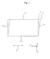
- the cross sectional shape of the vibrating piece 2 is deformed to a shape of a parallelogram (see dotted lines).
- unnecessary vibration component in the direction of z-axis is induced so that torsion vibration is induced in the detection vibration piece.
- Such noise component may be substantially changed depending on temperature to generate the zero point temperature drift.
- the deformation of the cross sectional shape of the vibration piece 2 is considered to be a cause of the drift.
- WD/TD exceeds 2.4, (when the width is too large in other words), torsion vibration component may be induced so that the unnecessary vibration component in Z-axis made considerable to increase the drift. It is thus necessary that WD/TD be not larger than 2.4.
- WD/TD when WD/TD is below 0.3 (when the width of the cross sectional shape is too narrow in other words), torsion vibration component may be induced so that the unnecessary vibration component in Z-azis made considerable to increase the drift. It is thus necessary that WD/TD be not smaller than 0.3.
- WD/TD may preferably be not smaller than 1.7 and more preferably be not smaller than 2.0 for further reducing the deviation of zero point temperature drift.
- the width WD of the driving vibration piece may preferably be not larger than 300 ⁇ m for improving the sensitivity. This width WD may preferably be not smaller than 200 ⁇ m for reducing the unnecessary vibration component.
- the thickness TD of the driving vibration piece may preferably be not larger than 150 ⁇ m for improving the sensitivity. This thickness TD may preferably be not smaller than 50 ⁇ m for reducing the unnecessary vibration component.
- WD/TD may preferably be not larger than 0.7 and more preferably be not larger than 0.6 for further reducing the deviation of zero point temperature drift.
- the width WD of the driving vibration piece may preferably be not smaller than 40 ⁇ m for improving the sensitivity.
- the width WD may preferably be not larger than 150 ⁇ m for reducing the unnecessary vibration component.
- the thickness TD of the driving vibration piece may preferably be not larger than 300 ⁇ m for improving the sensitivity. This thickness TD may preferably be not smaller than 100 ⁇ m for reducing the unnecessary vibration component.
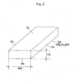
- the driving and detection vibration pieces are plate-shaped.
- the operational mode of the vibration pieces is not limited and may preferably be bending vibration mode.
- the vibration pieces may preferably be formed along a specified plane. In this case, it is not required that the vibration piece is formed along a specified plane in a geometrically strict meaning and production error is allowed.
- a vibrator may have the vibration pieces and the other parts which is not plate-shaped. In a preferred embodiment, the whole of the vibrator is plate shaped.
- the vibrator has surfaces 2c and 2d both substantially parallel with the specified plane (X-Y plane).
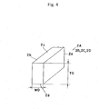
- detection vibration pieces 11A are bending vibration pieces each having a pair of surfaces 11c and 11d substantially parallel with each other and a pair of side faces 11a and 11b.
- a ratio (WT/TT) of the thickness WT to the thickness TT of the detection vibration piece is not smaller than 1.5 and not larger than 3.0. That is, also in the detection vibration piece, zero point temperature drift may be generated due to the torsion vibration component. It is found that such unnecessary vibration component may also be reduced by the present invention. On this point of view, it is possible to reduce the unnecessary vibration component in the direction of Z-axis by adjusting WT/TT at a value not smaller than 1.5, that is by applying a wider cross sectional shape.
- WT/TT exceeds 3.0 (the width becomes too large), the torsion vibration component become large so that zero point temperature drift may be increased.
- WT/TT may preferably be not larger than 3.0.
- WT/TT may preferably be not smaller than 1.7 and may more preferably be smaller than 2.0 for further reducing the change of zero point temperature drift. WT/TT may preferably be not larger than 2.5.
- the width WT of the detection vibration piece may preferably be not larger than 300 ⁇ m.
- WT may preferably be not smaller than 150 ⁇ m for reducing the unnecessary vibration component.
- the thickness TT of the detection vibration piece may preferably be not larger than 150 ⁇ m for improving the sensitivity.
- TT may preferably be not smaller than 50 ⁇ m for reducing the unnecessary vibration component.
- the inventors have successfully reduced the unnecessary vibration component in the direction of z-axis by adjusting WT/TT at a value not larger than 0.8 as shown in Fig. 5 .
- WT/TT When WT/TT is below 0.3 (the width becomes too small), the torsion vibration component become large so that zero point temperature drift may be increased.
- WT/TT may preferably be not smaller than 0.3.
- WT/TT may preferably be not larger than 0.7 and more preferably be not larger than 0.6 for reducing the deviation of zero point temperature drift.
- the width WT of the detection vibration piece may preferably be not smaller than 40 ⁇ m.
- WT may preferably be not larger than 150 ⁇ m for reducing the unnecessary vibration component.
- the thickness TT of the detection vibration piece may preferably be not larger than 300 ⁇ m for improving the sensitivity. TT may preferably be not smaller than 100 ⁇ m for reducing the unnecessary vibration component.
- the material of the vibrator is not particularly limited, and may preferably be a piezoelectric single crystal.
- the material may more preferably be a piezoelectric single crystal selected from the group consisting of quartz, lithium niobate, lithium tantalite, lithium niobate-lithium tantalite solid solution, lithium borate and langasite.
- the vibrator is made of a piezoelectric single crystal having three a-axes of tri-centrosymmetrical system in a specified plane and a c-axis in a direction perpendicular to the specified plane.
- the single crystal is preferably quartz.
- one side face is [2 1 1 0] face and the other side face is [ - ,2110] face.
- the shape of a protrusion formed on the other side face 2b may be considerably changed so that zero point temperature drift may be increased.
- the zero point temperature drift due to the deviation of output from the inventive vibrator may be affected by the cross sectional shape of the vibrator, irrelevant of a process for forming the vibrator.
- the process for forming the vibration pieces and vibrator according to the present invention is thus not particularly limited and may be wet etching, dry etching as well as laser beam processing.
- an etchant is not limited and may be as follows.
- the etchant may contain fluoric acid and may preferably be aqueous solution of fluoric acid or fluoric acid and ammonium fluoride mixed at an arbitrary ratio.
- the content of the etchant may preferably be not higher than 40 weight percent and the temperature of the etchant may preferably be 40 to 80 °C.
- the vibratory gyroscope according to the present invention has the vibrator as described above.
- the gyroscope further has a driving means and detecting means.
- the driving and detecting means are generally composed of electrodes formed on the vibrator, respectively.
- the vibratory gyroscope of the present invention measures a turning angular rate around a turning axis Z substantially perpendicular to the specified plane X-Y.
- each vibration piece is bent in bending vibration mode along the specified plane X-Y.
- the vibrator has a supporting part protruding from a base portion and the supporting part supports the driving vibration piece.
- Fig. 6 is a plan view showing a vibrator according to this embodiment of the present invention
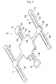
- Fig. 7 is a perspective view showing the vibrator.
- the vibrator 5 measures a turning angular rate around Z-axis substantially perpendicular to the specified plane (X-Y plane).
- the vibrator 5 has a fixing part 4B having a square shape of quad-symmetrical with respect to the center of gravity GO of the vibrator.
- Elongate supporting parts 6 are protruded from the edge of the fixing part 4B.
- a pair of driving vibration pieces 2A and 2B on z-axis are protruded from the tip part of each supporting part 6 in the direction perpendicular to the supporting part 6.
- the base part 30 of each driving vibration piece is protruded from the tip part of each supporting part so that the base part 30 may function as a fixing part for each driving vibration piece.
- Driving electrodes 7 are provided on each driving vibration piece.
- Elongate detection vibration piece 11A or 11B is protruded from the outer edge of the fixing part 4B.
- Detection vibration pieces 8 are provided on each of the detection vibration pieces.
- An weight portion 10 is provided on each of the detection vibration pieces 11A or 11B for detection.
- each of the driving vibration pieces 2A, 2B, 2C and 2D is vibrated in bending vibration mode as an arrow A around the base part 30.
- each supporting part 6 is vibrated in bending vibration mode circumferentially as an arrow C around the base part to the fixing part 4B. Responsive to this, each of the detection vibration pieces 11A and 11B is vibrated as an arrow B. Detection vibration induced in each of the detection vibration pieces 11A and 11B is measured to calculate a turning angular rate around Z-axis.
- each vibration piece has a weight or enlarged portion in the tip part, or, a groove or through hole therein.
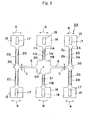
- Fig. 8 shows a vibrator 5A according to this embodiment
- Fig. 9 is a perspective view showing the vibrator 5A of Fig. 8 .
- elongate grooves 20 are formed in the surfaces 2c and 2d of each of the driving vibration pieces 2A, 2B, 2C and 2D.
- a driving electrode is formed in each groove 20.
- a weight part or enlarged part 15 is provided in the tip part of each of the detection vibration pieces 2A, 2B, 2C and 2D.
- a through hole 17 is formed in the weight or enlarged part 15.
- elongate grooves 21 are formed in the surfaces 11c and 11d of each of the detection vibration pieces 11A and 11B.
- a detection electrode is provided in the groove 21.
- an enlarged or weight part 16 is provided in the tip part of each of the detection vibration pieces 11A and 11B.
- a through hole 18 is formed in the weight part 16.
- the vibrator and vibratory gyroscope shown in Figs. 6 and 7 were produced. Specifically, chromium films of 200 angstroms in thickness and gold films of 1000 angstroms in thickness were formed in turns on a wafer made of a Z-plate of quartz with a predetermined thickness. Both main faces of the wafer were coated with resist films, respectively, and photo masks were mounted for exposing light.
- the wafer was then immersed in aqueous solution of iodine and potassium iodide to remove excessive gold in the gold film by etching, and was further immersed in aqueous solution of cerium-ammonium nitrate and perchloric acid to remove excessive chromium in the chromium film by etching.
- the wafer was etched by immersing the wafer in ammonium bifluoride at a temperature of 80 °C for 20 hours to form the external shape of the vibrator 5.
- Aluminum films each having a thickness of 2000 angstrom was formed as electrode films 7 and 8 using a metal mask.
- the thus obtained vibrator 5 had a fixing part 4B with a length of 6.0 mm and a width of 6.0 mm.
- Each of the driving vibration pieces 2A, 2B, 2C and 2D had a length of 6.0 mm.
- Each of the detection vibration pieces 11A and 11B had a length of 6.0 mm.
- Each detecting electrode 8 had a length of 2.8 mm.
- the width WD and thickness TD of each of the driving vibration pieces 2A, 2B, 2C and 2D, and the ratio (WD/TD) were changed as shown in table 1.
- the ratio (WT/TT) of the width WT to thickness TT of each of the detection vibration pieces 11A and 11B was adjusted at 1.9.
- a supporting hole having a length of 0.75 mm and width of 0.75 mm was formed in the central part of the fixing part 4B of the vibrator.
- a metal pin with a diameter of 0.6 mm was inserted through the hole.
- the vibrator was adhered with the metal pin with a silicone resin adhesive.
- the thus obtained vibratory gyroscope was subjected to measurement of the zero point signal of the detection signal within a temperature range of minus 40 °C to plus 80 °C.
- Vibratory gyroscopes were produced according to the same process as the experiment 1 and subjected to measurement of the zero point temperature drift. Different from the experiment 1, the ratio (WD/TD) of the width WD to thickness TD of each of the driving vibration pieces 2A, 2B, 2C and 2D was adjusted at 2.0. The width WT, thickness TT and ratio (WT/TT) of each of the detection vibration pieces 11A and 11B were changed as shown in table 2.
- the vibrator and vibratory gyroscope shown in Figs. 8 and 9 were produced. Specifically, chromium films of 200 angstroms in thickness and gold films of 1000 angstroms in thickness were formed in turns on a wafer made of a Z-plate of quartz with a predetermined thickness. Both main faces of the wafer were coated with resist films, respectively, and photo masks were mounted for exposing light.
- the wafer was then immersed in aqueous solution of iodine and potassium iodide to remove excessive gold in the gold film by etching, and was further immersed in aqueous solution of cerium-ammonium nitrate and perchloric acid to remove excessive chromium in the chromium film by etching.
- the wafer was etched by immersing the wafer in ammonium bifluoride at a temperature of 80 °C for 20 hours to form the external shape of the vibrator 5A. Resists on both faces of the wafer were removed and the wafer was then immersed in ammonium bifluoride at a temperature of 80 °C for 30 minutes to half etch the wafer. The grooves 20 and 21 were thus formed in the vibrator 5A.
- Chromium films of 200 angstroms in thickness and gold films of 1000 angstroms in thickness were formed in turns on the wafer by means of vapor deposition. Both main faces of the wafer were coated with resist films, respectively, and photo masks were mounted for exposing light. The wafer was then immersed in aqueous solution of iodine and potassium iodide to remove excessive gold in the gold film by etching, and was further immersed in aqueous solution of cerium-ammonium nitrate and perchloric acid to remove excessive chromium in the chromium film by etching. The electrode films 7 and 8 were thus formed.
- the thus obtained vibrator 5A had a fixing part 4B with a length of 0.4 mm and a width of 0.4 mm.
- Each of the driving vibration pieces 2A, 2B, 2C and 2D had a length of 1.0 mm.
- Each of the detection vibration pieces 11A and 11B had a length of 0.8 mm.
- Each detecting electrode 8 had a length of 0.5 mm.
- the width WD and thickness TD of each of the driving vibration pieces 2A, 2B, 2C and 2D, and the ratio (WD/TD) were changed as shown in table 3.
- the ratio (WT/TT) of the width WT to thickness TT of each of the detection vibration pieces 11A and 11B was adjusted at 0.5.
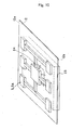
- the vibrator 5 is fixed as shown in Figs. 10 and 11 . That is, the substrate 22 has a shape of a flat plate having one and the other opposing faces 12a and 12b.
- the vibrator 5 or 5A is supported at its lower face with bonding wires 24 over the one face 12a.
- the bonding wire 24 is electrically connected with electrodes (not shown) on the vibrator 5 or 5A.
- a semiconductor integrated circuit chip 23 is supported on the other face 12b with bonding wires 25.
- the electrode terminals on the vibrator 5 or 5A and the terminals of the chip 23 are connected with the electrodes on the substrate 12 by means of bonding wires, respectively.
- the vibrator 5 or 5A and chip 23 are provided at positions overlapping with each other viewed in the direction of thickness of the substrate 12.
- the substrate 12 of the present example is a so-called flexible substrate.
- the thus obtained vibratory gyroscope was subjected to measurement of the zero point signal of the detection signal within a temperature range of minus 40 °C to + 80 °C.
- 10 vibrators were produced as described above and subjected to the above measurement.
- a difference of the maximum and minimum values of the zero point signal between minus 40 °C and plus 85 °C was calculated to obtain a zero point temperature drift.
- the standard deviation of the drift for 10 vibrators was also shown in table 3.
- Vibratory gyroscopes were produced according to the same process as the experiment 3 and subjected to measurement of the zero point temperature drift. Different from the experiment 3, the ratio (WD/TD) of the width WD to thickness TD of each of the driving vibration pieces 2A, 2B, 2C and 2D at 0.5. The width WT, thickness TT and ratio (WT/TT) of each of the detection vibration pieces 11A and 11B were changed as shown in table 4.
- the vibrator of the experiment 1 was prepared except that the ratio of width to thickness of each driving vibration piece is variously changed.
- the displacement on z-axis was simulated and the results were shown in Fig. 12 .
- the vertical axis shows the displacement on the z-axis (unnecessary displacement) and the horizontal axis shows the ratio of width/thickness of the driving vibration piece.
- the driving frequency of the driving vibration was set at 45 kHz and applied voltage was set at 1 volt. It was thus proved that the displacement on the z-axis may be considerably reduced within the range of the present invention. It is considered that the reduction of displacement may contribute to the reduction of the zero point temperature drift.
- the zero point temperature drift of a vibrator and the deviation or change of the drift among vibrators fabricated may be reduced according to the present invention.
- the present invention has been explained referring to the preferred embodiments, however, the present invention is not limited to the illustrated embodiments which are given by way of examples only, and may be carried out in various modes without departing from the scope of the invention.
Landscapes
- Physics & Mathematics (AREA)
- Engineering & Computer Science (AREA)
- General Physics & Mathematics (AREA)
- Radar, Positioning & Navigation (AREA)
- Remote Sensing (AREA)
- Gyroscopes (AREA)
Applications Claiming Priority (3)
| Application Number | Priority Date | Filing Date | Title |
|---|---|---|---|
| JP2002068862 | 2002-03-13 | ||
| JP2003028600A JP4305623B2 (ja) | 2002-03-13 | 2003-02-05 | 振動子および振動型ジャイロスコープ |
| EP03005604A EP1345008A3 (de) | 2002-03-13 | 2003-03-12 | Vibratoren und Vibrationskreisel |
Related Parent Applications (2)
| Application Number | Title | Priority Date | Filing Date |
|---|---|---|---|
| EP03005604A Division EP1345008A3 (de) | 2002-03-13 | 2003-03-12 | Vibratoren und Vibrationskreisel |
| EP03005604.8 Division | 2003-03-12 |
Publications (3)
| Publication Number | Publication Date |
|---|---|
| EP2620747A2 true EP2620747A2 (de) | 2013-07-31 |
| EP2620747A3 EP2620747A3 (de) | 2014-07-02 |
| EP2620747B1 EP2620747B1 (de) | 2018-12-26 |
Family
ID=27767230
Family Applications (2)
| Application Number | Title | Priority Date | Filing Date |
|---|---|---|---|
| EP13165482.4A Expired - Lifetime EP2620747B1 (de) | 2002-03-13 | 2003-03-12 | Vibrator und Vibrationskreisel |
| EP03005604A Withdrawn EP1345008A3 (de) | 2002-03-13 | 2003-03-12 | Vibratoren und Vibrationskreisel |
Family Applications After (1)
| Application Number | Title | Priority Date | Filing Date |
|---|---|---|---|
| EP03005604A Withdrawn EP1345008A3 (de) | 2002-03-13 | 2003-03-12 | Vibratoren und Vibrationskreisel |
Country Status (3)
| Country | Link |
|---|---|
| US (1) | US6698292B2 (de) |
| EP (2) | EP2620747B1 (de) |
| JP (1) | JP4305623B2 (de) |
Families Citing this family (37)
| Publication number | Priority date | Publication date | Assignee | Title |
|---|---|---|---|---|
| AU4056799A (en) * | 1999-05-31 | 2000-12-18 | Nanomotion Ltd. | Multilayer piezoelectric motor |
| WO2001063679A1 (en) * | 2000-02-24 | 2001-08-30 | Nanomotion Ltd. | Resonance shifting |
| JP4389480B2 (ja) * | 2003-05-28 | 2009-12-24 | セイコーエプソン株式会社 | 振動子の支持機構及び振動子ユニット |
| JP4163067B2 (ja) | 2003-07-14 | 2008-10-08 | 日本碍子株式会社 | 物理量測定方法および装置 |
| JP4352975B2 (ja) * | 2003-07-25 | 2009-10-28 | セイコーエプソン株式会社 | 圧電振動片、圧電振動片の支持構造、圧電振動子及び振動型圧電ジャイロスコープ |
| CN1879007B (zh) * | 2003-11-12 | 2010-09-08 | 精工爱普生株式会社 | 振动式陀螺仪 |
| US7140251B2 (en) * | 2004-05-19 | 2006-11-28 | Ngk Insulators, Ltd. | Devices for measuring physical values and vibrators |
| KR100618342B1 (ko) * | 2004-07-29 | 2006-09-04 | 삼성전자주식회사 | 소형 구조물 및 그 제작방법 |
| JP4381354B2 (ja) * | 2004-09-10 | 2009-12-09 | セイコーエプソン株式会社 | 振動子の支持構造および物理量測定装置 |
| JP4428309B2 (ja) * | 2004-09-10 | 2010-03-10 | セイコーエプソン株式会社 | 振動型ジャイロスコープ |
| JP2006105614A (ja) * | 2004-09-30 | 2006-04-20 | Seiko Epson Corp | 振動型ジャイロスコープ、及び振動型ジャイロスコープの製造方法 |
| ATE374355T1 (de) | 2004-12-20 | 2007-10-15 | Eta Sa Mft Horlogere Suisse | Wandler zur winkelgeschwindigkeitsmessung |
| JP4415382B2 (ja) * | 2005-01-20 | 2010-02-17 | セイコーエプソン株式会社 | 振動ジャイロ素子、振動ジャイロ素子の支持構造およびジャイロセンサ |
| JP2006201053A (ja) * | 2005-01-21 | 2006-08-03 | Seiko Epson Corp | 圧電振動ジャイロ素子、圧電振動ジャイロ素子の支持構造およびジャイロセンサ |
| JP2006201118A (ja) * | 2005-01-24 | 2006-08-03 | Seiko Epson Corp | 圧電振動ジャイロ素子およびジャイロセンサ |
| JP4415383B2 (ja) * | 2005-01-24 | 2010-02-17 | セイコーエプソン株式会社 | 振動ジャイロ素子、振動ジャイロ素子の支持構造およびジャイロセンサ |
| US7554343B2 (en) * | 2005-07-25 | 2009-06-30 | Piezoinnovations | Ultrasonic transducer control method and system |
| US20090064783A1 (en) * | 2006-01-24 | 2009-03-12 | Matsushita Electric Industrial Co., Ltd. | Inertial force sensor |
| JP4924873B2 (ja) * | 2006-08-02 | 2012-04-25 | セイコーエプソン株式会社 | 圧電振動ジャイロモジュール及び圧電振動ジャイロセンサ |
| JP5205725B2 (ja) * | 2006-08-21 | 2013-06-05 | パナソニック株式会社 | 角速度センサ |
| WO2008059757A1 (en) * | 2006-11-14 | 2008-05-22 | Panasonic Corporation | Sensor |
| JP2008139054A (ja) * | 2006-11-30 | 2008-06-19 | Epson Toyocom Corp | 角速度センサ |
| JP2008157810A (ja) * | 2006-12-25 | 2008-07-10 | Tdk Corp | 角速度センサ素子および角速度センサ装置 |
| JP4915246B2 (ja) * | 2007-01-26 | 2012-04-11 | セイコーエプソン株式会社 | ジャイロモジュール |
| JP4893335B2 (ja) * | 2007-01-26 | 2012-03-07 | セイコーエプソン株式会社 | ジャイロモジュール |
| US8117914B2 (en) * | 2007-02-20 | 2012-02-21 | Panasonic Corporation | Inertia force sensor and composite sensor for detecting inertia force |
| JP4395171B2 (ja) * | 2007-02-23 | 2010-01-06 | 多摩川精機株式会社 | 角速度センサおよびその製造方法 |
| JP2008249489A (ja) * | 2007-03-30 | 2008-10-16 | Tdk Corp | 角速度センサ素子および角速度センサ装置 |
| US8446079B2 (en) * | 2008-05-23 | 2013-05-21 | Statek Corporation | Piezoelectric resonator with vibration isolation |
| WO2010019278A1 (en) * | 2008-08-15 | 2010-02-18 | Sural | Solid-state inertial sensor on chip |
| EP2330381A4 (de) | 2008-10-07 | 2012-07-04 | Panasonic Corp | Winkelgeschwindigkeitssensorelement, winkelgeschwindigkeitssensor und winkelgeschwindigkeitssensoreinheit mit dem winkelgeschwindigkeitssensorelement sowie signalerkennungsverfahren für die winkelgeschwindigkeitssensoreinheit |
| JP2010190706A (ja) * | 2009-02-18 | 2010-09-02 | Panasonic Corp | 慣性力センサ |
| CN102725606A (zh) * | 2010-01-29 | 2012-10-10 | 松下电器产业株式会社 | 角速度传感器 |
| JP2011220997A (ja) * | 2010-03-26 | 2011-11-04 | Seiko Epson Corp | 物理量検出素子、物理量検出装置、および電子機器 |
| JP5838543B2 (ja) * | 2010-09-30 | 2016-01-06 | セイコーエプソン株式会社 | センサーデバイス、モーションセンサー、および電子機器 |
| JP2015087262A (ja) * | 2013-10-31 | 2015-05-07 | セイコーエプソン株式会社 | 振動素子、振動子、電子機器および移動体 |
| US10690500B2 (en) * | 2017-03-28 | 2020-06-23 | Seiko Epson Corporation | Sensor element, sensor, electronic apparatus, and vehicle |
Citations (1)
| Publication number | Priority date | Publication date | Assignee | Title |
|---|---|---|---|---|
| JP2001012952A (ja) | 1999-07-01 | 2001-01-19 | Ngk Insulators Ltd | 振動系、振動子および振動型ジャイロスコープ |
Family Cites Families (8)
| Publication number | Priority date | Publication date | Assignee | Title |
|---|---|---|---|---|
| JPH07113645A (ja) * | 1993-10-15 | 1995-05-02 | Toyota Motor Corp | 振動ジャイロ |
| US5824900A (en) * | 1995-04-04 | 1998-10-20 | Matsushita Electric Industrial Co., Ltd. | Angular velocity sensor |
| JPH1054726A (ja) * | 1996-08-08 | 1998-02-24 | Murata Mfg Co Ltd | 振動ジャイロおよびその製造方法 |
| CA2241929A1 (en) * | 1996-10-29 | 1998-05-07 | Mitsui Chemicals, Incorporated | Vibration gyroscope |
| JP3285140B2 (ja) * | 1997-09-04 | 2002-05-27 | 株式会社村田製作所 | 振動ジャイロの調整方法 |
| JP3844784B2 (ja) * | 1997-09-08 | 2006-11-15 | 日本碍子株式会社 | 圧電/電歪デバイス |
| US6397667B1 (en) * | 1997-12-26 | 2002-06-04 | Mitutoyo Corporation | Surface property measuring device |
| US6621194B1 (en) * | 1999-11-15 | 2003-09-16 | Matsushita Electric Industrial Co., Ltd. | Piezoelectric element having thickness shear vibration and mobile communication device using the same |
-
2003
- 2003-02-05 JP JP2003028600A patent/JP4305623B2/ja not_active Expired - Lifetime
- 2003-03-10 US US10/384,958 patent/US6698292B2/en not_active Expired - Lifetime
- 2003-03-12 EP EP13165482.4A patent/EP2620747B1/de not_active Expired - Lifetime
- 2003-03-12 EP EP03005604A patent/EP1345008A3/de not_active Withdrawn
Patent Citations (1)
| Publication number | Priority date | Publication date | Assignee | Title |
|---|---|---|---|---|
| JP2001012952A (ja) | 1999-07-01 | 2001-01-19 | Ngk Insulators Ltd | 振動系、振動子および振動型ジャイロスコープ |
Also Published As
| Publication number | Publication date |
|---|---|
| JP4305623B2 (ja) | 2009-07-29 |
| US20030177836A1 (en) | 2003-09-25 |
| JP2003337025A (ja) | 2003-11-28 |
| EP2620747B1 (de) | 2018-12-26 |
| EP1345008A3 (de) | 2012-02-15 |
| EP1345008A2 (de) | 2003-09-17 |
| EP2620747A3 (de) | 2014-07-02 |
| US6698292B2 (en) | 2004-03-02 |
Similar Documents
| Publication | Publication Date | Title |
|---|---|---|
| EP2620747B1 (de) | Vibrator und Vibrationskreisel | |
| EP1498693B1 (de) | Verfahren und Vorrichtungen zum Messen physikalischer Grössen | |
| EP1898180B1 (de) | Vibratoren und Vibrationskreisel | |
| KR100906178B1 (ko) | 진동자의 지지 구조 및 물리량 측정 장치 | |
| US20140152153A1 (en) | Piezoelectric resonating device, manufacturing method thereof, piezoelectric resonator, and piezoelectric oscillator | |
| US7150386B2 (en) | Systems and structures for supporting vibrators | |
| CN1938944B (zh) | 石英晶体振荡器的制造方法 | |
| US7278313B2 (en) | Structures for supporting vibrators and devices for measuring physical quantities | |
| EP1030164B1 (de) | Vibrationskreisel und ihre Herstellungsverfahren | |
| EP1496337B1 (de) | Vibrationskreisel mit Strukturen zur Halterung des Schwingers | |
| JP2004226181A (ja) | 振動ジャイロ | |
| EP1684047B1 (de) | Trägerglied eines vibrators | |
| JP2007108053A (ja) | 振動子および振動型ジャイロスコープ用測定素子 | |
| JP2003207338A (ja) | 振動型ジャイロスコープ用振動子および振動型ジャイロスコープ | |
| JP4067044B2 (ja) | 振動子および振動型ジャイロスコープ | |
| JP3856108B2 (ja) | 振動型ジャイロスコープ用振動子および振動型ジャイロスコープ | |
| JP2003315048A (ja) | 振動片、振動子、振動型ジャイロスコープおよび振動片の製造方法 | |
| JP2003240558A (ja) | 振動子および振動型ジャイロスコープ |
Legal Events
| Date | Code | Title | Description |
|---|---|---|---|
| PUAI | Public reference made under article 153(3) epc to a published international application that has entered the european phase |
Free format text: ORIGINAL CODE: 0009012 |
|
| AC | Divisional application: reference to earlier application |
Ref document number: 1345008 Country of ref document: EP Kind code of ref document: P |
|
| AK | Designated contracting states |
Kind code of ref document: A2 Designated state(s): DE FR GB |
|
| PUAL | Search report despatched |
Free format text: ORIGINAL CODE: 0009013 |
|
| AK | Designated contracting states |
Kind code of ref document: A3 Designated state(s): DE FR GB |
|
| RIC1 | Information provided on ipc code assigned before grant |
Ipc: G01C 19/56 20120101AFI20140527BHEP |
|
| 17P | Request for examination filed |
Effective date: 20141229 |
|
| RBV | Designated contracting states (corrected) |
Designated state(s): DE FR GB |
|
| 17Q | First examination report despatched |
Effective date: 20170302 |
|
| GRAP | Despatch of communication of intention to grant a patent |
Free format text: ORIGINAL CODE: EPIDOSNIGR1 |
|
| INTG | Intention to grant announced |
Effective date: 20180629 |
|
| GRAS | Grant fee paid |
Free format text: ORIGINAL CODE: EPIDOSNIGR3 |
|
| GRAA | (expected) grant |
Free format text: ORIGINAL CODE: 0009210 |
|
| AC | Divisional application: reference to earlier application |
Ref document number: 1345008 Country of ref document: EP Kind code of ref document: P |
|
| AK | Designated contracting states |
Kind code of ref document: B1 Designated state(s): DE FR GB |
|
| REG | Reference to a national code |
Ref country code: GB Ref legal event code: FG4D |
|
| REG | Reference to a national code |
Ref country code: DE Ref legal event code: R096 Ref document number: 60351738 Country of ref document: DE |
|
| PGFP | Annual fee paid to national office [announced via postgrant information from national office to epo] |
Ref country code: GB Payment date: 20190325 Year of fee payment: 17 Ref country code: FR Payment date: 20190326 Year of fee payment: 17 |
|
| REG | Reference to a national code |
Ref country code: DE Ref legal event code: R097 Ref document number: 60351738 Country of ref document: DE |
|
| PLBE | No opposition filed within time limit |
Free format text: ORIGINAL CODE: 0009261 |
|
| STAA | Information on the status of an ep patent application or granted ep patent |
Free format text: STATUS: NO OPPOSITION FILED WITHIN TIME LIMIT |
|
| 26N | No opposition filed |
Effective date: 20190927 |
|
| PG25 | Lapsed in a contracting state [announced via postgrant information from national office to epo] |
Ref country code: FR Free format text: LAPSE BECAUSE OF NON-PAYMENT OF DUE FEES Effective date: 20200331 |
|
| GBPC | Gb: european patent ceased through non-payment of renewal fee |
Effective date: 20200312 |
|
| PG25 | Lapsed in a contracting state [announced via postgrant information from national office to epo] |
Ref country code: GB Free format text: LAPSE BECAUSE OF NON-PAYMENT OF DUE FEES Effective date: 20200312 |
|
| PGFP | Annual fee paid to national office [announced via postgrant information from national office to epo] |
Ref country code: DE Payment date: 20220203 Year of fee payment: 20 |
|
| REG | Reference to a national code |
Ref country code: DE Ref legal event code: R071 Ref document number: 60351738 Country of ref document: DE |