EP2620945B1 - Structure et procédé de réparation du diélectrique de tunnel de cellules de mémoire non-volatiles - Google Patents
Structure et procédé de réparation du diélectrique de tunnel de cellules de mémoire non-volatiles Download PDFInfo
- Publication number
- EP2620945B1 EP2620945B1 EP13151698.1A EP13151698A EP2620945B1 EP 2620945 B1 EP2620945 B1 EP 2620945B1 EP 13151698 A EP13151698 A EP 13151698A EP 2620945 B1 EP2620945 B1 EP 2620945B1
- Authority
- EP
- European Patent Office
- Prior art keywords
- healing
- memory cells
- tunnel dielectric
- voltage
- healing process
- Prior art date
- Legal status (The legal status is an assumption and is not a legal conclusion. Google has not performed a legal analysis and makes no representation as to the accuracy of the status listed.)
- Active
Links
Images


Classifications
-
- G—PHYSICS
- G11—INFORMATION STORAGE
- G11C—STATIC STORES
- G11C16/00—Erasable programmable read-only memories
- G11C16/02—Erasable programmable read-only memories electrically programmable
- G11C16/04—Erasable programmable read-only memories electrically programmable using variable threshold transistors, e.g. FAMOS
- G11C16/0408—Erasable programmable read-only memories electrically programmable using variable threshold transistors, e.g. FAMOS comprising cells containing floating gate transistors
- G11C16/0416—Erasable programmable read-only memories electrically programmable using variable threshold transistors, e.g. FAMOS comprising cells containing floating gate transistors comprising cells containing a single floating gate transistor and no select transistor, e.g. UV EPROM
-
- G—PHYSICS
- G11—INFORMATION STORAGE
- G11C—STATIC STORES
- G11C16/00—Erasable programmable read-only memories
- G11C16/02—Erasable programmable read-only memories electrically programmable
- G11C16/04—Erasable programmable read-only memories electrically programmable using variable threshold transistors, e.g. FAMOS
- G11C16/0483—Erasable programmable read-only memories electrically programmable using variable threshold transistors, e.g. FAMOS comprising cells having several storage transistors connected in series
-
- G—PHYSICS
- G11—INFORMATION STORAGE
- G11C—STATIC STORES
- G11C16/00—Erasable programmable read-only memories
- G11C16/02—Erasable programmable read-only memories electrically programmable
- G11C16/06—Auxiliary circuits, e.g. for writing into memory
- G11C16/34—Determination of programming status, e.g. threshold voltage, overprogramming or underprogramming, retention
- G11C16/349—Arrangements for evaluating degradation, retention or wearout, e.g. by counting erase cycles
-
- H—ELECTRICITY
- H10—SEMICONDUCTOR DEVICES; ELECTRIC SOLID-STATE DEVICES NOT OTHERWISE PROVIDED FOR
- H10D—INORGANIC ELECTRIC SEMICONDUCTOR DEVICES
- H10D64/00—Electrodes of devices having potential barriers
- H10D64/01—Manufacture or treatment
- H10D64/031—Manufacture or treatment of data-storage electrodes
- H10D64/035—Manufacture or treatment of data-storage electrodes comprising conductor-insulator-conductor-insulator-semiconductor structures
Definitions
- This disclosure relates generally to non-volatile memories, and more specifically, to healing tunnel dielectrics of non-volatile memory cells.
- Non-volatile memories have a limited life due to a limited number of cycles, which is called endurance, and to a limited amount of time that the NVM can retain data, which is called data retention.
- Data retention is primarily related to how well the charge in a floating gate of an NVM cell is retained in the floating gate. There is a point at which enough charge has leaked out of the floating gate that the state of the NVM cell cannot be reliably detected.
- endurance after enough cycles of programming and erasing, charge is not easily placed into the floating gate or removed from the floating gate.
- the basic notion of healing is desirable because it can potentially be used to improve an NVM made using an existing process. Thus, whatever improvements made by the healing are additive to improvements in the processing.
- US 2010/025811 A1 discloses an integrated circuit device that includes structures that exhibit performance degradation as a function of use (e.g., accumulated defects within the tunnelling oxide of a Flash memory cell, or trapped charge within a charge storage layer) and heating circuitry disposed in proximity to the structures to heat the structures to a temperature that reverses the degradation.
- the word lines or the bit lines of the memory device are used as heating elements.
- US 5930173 A1 discloses a method of initializing a flash EEPROM.
- the method comprises a preprogramming operation of a predetermined data that is first performed in a plurality of memory cells of a memory cell array and then an erasing operation is performed to the plurality of memory cells. Then, a verifying operation of whether the erasing operation is correctly performed is performed. During an initializing operation composed of the pre-programming operation, the erasing operation and the verifying operation, electrons or holes trapped in a tunnel oxide film are pulled out.
- the present invention provides a semiconductor device as defined in independent device claim 1, wherein advantageous embodiments are defined in dependent claims 2-6.
- Tunnel dielectric healing is achieved using a drain voltage that is higher than the control gate voltage, the well voltage, and the source voltage. This approach is effective in drawing electrons that have been trapped in the tunnel dielectric out of the tunnel dielectric and thereby improving endurance and data retention.
- the semiconductor substrate described herein can be any semiconductor material or combinations of materials, such as gallium arsenide, silicon germanium, silicon-on-insulator (SOI), silicon, monocrystalline silicon, the like, and combinations of the above.
- SOI silicon-on-insulator
- bus is used to refer to a plurality of signals or conductors which may be used to transfer one or more various types of information, such as data, addresses, control, or status.
- the conductors as discussed herein may be illustrated or described in reference to being a single conductor, a plurality of conductors, unidirectional conductors, or bidirectional conductors. However, different embodiments may vary the implementation of the conductors. For example, separate unidirectional conductors may be used rather than bidirectional conductors and vice versa.
- plurality of conductors may be replaced with a single conductor that transfers multiple signals serially or in a time multiplexed manner. Likewise, single conductors carrying multiple signals may be separated out into various different conductors carrying subsets of these signals. Therefore, many options exist for transferring signals.
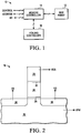
- FIG. 1 Shown in FIG. 1 is a non-volatile memory (NVM) 10 having an NVM array 12, a memory controller 14, and a healing controller 16.
- Memory controller 14 and array 12 are connected by a bus.
- Healing controller 16 is a connected to memory controller 14 by a bus.
- Memory controller 14 inputs and outputs data using a bus and receives control signals from a bus and addresses from a bus.
- Memory controller 14 controls what data is written into and read out from NVM array 12 using the control, address, and I/O signals.
- the writing is typically called programming for NVMs and, in the case of NVM 12 being a flash memory, NVM cells are erased in large blocks in preparation for being programmed.
- Writing data includes both erasing and programming and thus is often referenced as a program/erase cycle.
- Healing controller 16 monitors the operation of memory controller 14 and indicates to memory controller 14 when a healing operation is to be performed.
- NVM cell 18 representative of the memory cells of NVM array 12.
- NVM cell 18 is a floating gate type NVM cell having a control gate 20, an interface dielectric 22 under control gate 20, a floating gate 24 under interface dielectric 22, a tunnel dielectric 26 under floating gate 24, a channel region in a semiconductor layer 32 under tunnel dielectric 26, a source 28 in semiconductor layer 32 substantially aligned to a first side of floating gate 24, and a drain substantially aligned to a second side of floating gate 24.
- Control gate 20 is substantially aligned to source 28 and drain 30 also.
- the channel region is between source 28 and drain 30.
- Semiconductor layer 32 may be formed in a semiconductor substrate.
- An effective way of achieving desired characteristics of semiconductor layer 32 is to dope the substrate to a desired conductivity type and concentration for use in forming NVM cells.
- One way to achieve this is to begin with a P-type substrate, form an N-type well in the P-type substrate, and then form a P well within the N well whereby the P well is isolated from the substrate.
- semiconductor layer 32 may be referenced as a well and, because the typical preference is that the conductivity type be P, more specifically as P well 32.
- Terminals are connected control gate 20, source 28, drain 30, and P well 32 so that a selected control gate voltage VCG, a selected source voltage VS, a selected drain voltage VD, and a selected well voltage VPW may be applied to them, respectively. Shown in FIG.
- stage 34 is a stage 34, a stage 36, and a stage 38 of tunnel dielectric 26 as program/erase cycles are performed.
- stage 34 minimal program/erase cycles have been performed and there is no discernible charge trapping in tunnel dielectric 26.
- charge trapping has occurred that has begun to affect endurance and data retention as shown in stage 36.
- stage 38 of FIG. 3 After a healing cycle has been performed, the charge trapping has been significantly reduced as shown in stage 38 of FIG. 3 .
- Shown in FIG. 4 is a plot of the number of erase pulses required to achieve erasure of the NVM array versus the number of program/erase cycles and the result of a first healing, a second healing, and a third healing.
- the number of pulses per cycle increases very slowly and then begins to increase exponentially.
- the first healing is performed which brings the number of pulses per cycle to the nearly the same level as at the beginning.
- the dotted lines show that the erase pulses per cycle will continue to increase in the absence of the first healing.
- a similar situation to that at the beginning commences after the first healing in which the erase pulses per cycle slightly increases then again begins increasing exponentially.
- a second healing is then performed after about another 20,000 more cycles. This may be shortened as needed to ensure that the erase pulses per cycle is about the same as for the timing of the first healing.
- a third healing is then performed with similar results for the first and second healing.
- Shown in FIG. 5 is a plot of the number of program pulses required to achieve programming of cells NVM array 12 versus the number of program/erase cycles and the result of the first healing, the second healing, and the third healing.
- the number of pulses per cycle increases very slowly and then begins to increase exponentially.
- the first healing is performed which brings the number of pulses per cycle to the nearly the same level as at the beginning.
- the dotted lines show that the program pulses per cycle will continue to increase in the absence of the first healing.
- a similar situation to that at the beginning commences after the first healing in which the program pulses per cycle slightly increases then again begins increasing exponentially.
- a second healing is then performed after about another 20,000 more cycles. This may be shortened as needed to ensure that the program pulses per cycle is about the same as for the timing of the first healing.
- a third healing is then performed with similar results for the first and second healing.
- FIG. 6 Shown in FIG. 6 is a table showing the conditions for source voltage VS, drain voltage VD, control gate voltage VCG, and P well voltage VPW as applied by memory controller 14.
- source voltage VS is applied at ground
- drain voltage VD is at 4.5 volts
- control gate voltage VCG is applied at 9.0 volts
- well voltage VPW is applied at ground. This provides for current flow from drain to source in which the positive control gate voltage attracts electrons to the floating gate by hot carrier injection. Pulses are applied at these conditions until desired programming has been reached. Each such pulse is considered one of the pulses in a program/erase cycle. Programming and erasing are performed in response to control signals.
- source 28 and drain 30 are untied, control gate voltage VCG is applied at negative 9.0 (-9.0) volts, and well voltage VPW is stepped from 4.2 up to 9.0 volts. Each step is considered one of the pulses in the program/erase cycle.
- VCG negative 9.0 (-9.0) volts
- well voltage VPW is stepped from 4.2 up to 9.0 volts. Each step is considered one of the pulses in the program/erase cycle.
- With up to an 18 volt differential between P well 32 and control gate 20 electrons are pulled from floating gate to P well 32 by Fowler-Nordheim tunneling.
- Source 28 and drain 30 will naturally fall to a P/N junction drop below the positive voltage applied at P well 32 which will be about 8.3 volts in this case.
- source voltage VS For healing, which is in response to signals from healing controller 16, source voltage VS, control gate voltage VCG, and well voltage VPW are applied at ground, and drain voltage VD is applied at 4.5 volts.
- source voltage VS control gate voltage VCG, and well voltage VPW are applied at ground, and drain voltage VD is applied at 4.5 volts.
- drain voltage VD is applied at 4.5 volts.
- the result is that a high percentage of electrons are drawn from tunnel dielectric 26 and also holes are pushed out of tunnel dielectric 26.
- the healing procedure takes advantage of an elevated temperature at the junction between drain 30 and P well 32.
- Alternative techniques for determining when a healing step should be performed include simply performing a healing step after every set number of cycles, reducing the number of cycles between healing steps for each additional healing step, and performing a healing step when the number of erase/program pulses per cycle reaches a certain level. This may be for a single NVM cell or for an average or for some small set number such as ten NVM cells that exceed a predetermined pulse count. Another possibility is to base the healing steps on time or some combination of time with one of the above criteria. For example, perform a healing step every 20,000 cycles or after 6 months if the 20,000 cycles had not occurred within the 6 months.
- the detection that it is time for a healing step does not necessarily mean that it needs to be done immediately.
- Power down may be the preferred time to perform a healing step. In such case, assuming that power is still available, the performance of the healing step can be done after it appears the device has shut down.
- typically power is still available when the vehicle is turned off so the healing step can be performed when the vehicle is turned off.
- It may be necessary to have a memory available to temporarily store the information in the NVM during the healing step.
- the random access memory is not expected to be actively storing data in which case the random access memory can be used to store the NVM data during the healing step.
- each of the memory cells includes a tunnel dielectric, a well region including a first current electrode, a second current electrode, and a channel region between the first current electrode and the second current electrode, a floating gate wherein the tunnel dielectric is over the channel region and the floating gate is over the tunnel dielectric, an interface dielectric over the floating gate, and a control gate over the interface dielectric.
- the semiconductor device further includes a controller coupled to the memory cells, wherein the controller includes logic to determine when to perform a healing process in the tunnel dielectric of the memory cells, and to apply a first voltage to the first current electrode of the memory cells during the healing process to remove trapped electrons and holes from the tunnel dielectric.
- the semiconductor device may further include logic to apply another voltage to the second current electrode and a control gate during the healing process.
- the semiconductor device may have a further characterization by which the controller includes logic to apply another voltage to the well region during the healing process.
- the semiconductor device may have a further characterization by which the healing process takes advantage of an elevated temperature at a junction between the first current electrode and the well region.
- the semiconductor device may further include logic to perform the healing process after a threshold number of program and erase cycles.
- the semiconductor device may further include logic to perform subsequent healing processes after successively reduced numbers of program and erase cycles.
- the semiconductor device may further include logic to perform the healing process when a threshold number of pulses are required to erase the memory cells.
- the semiconductor device may further include logic to perform the healing process once a threshold number of pulses are required to program the memory cells.
- the semiconductor device may have a further characterization by which the controller is further operable to perform the healing process after the memory cells have operated over a specified number of program/erase cycles.
- the method may further include applying a second voltage to a second current electrode of the semiconductor memory cell.
- the method may further include applying other voltages to a second current electrode, a control gate, and a well region of the semiconductor memory cell during the healing process.
- the method may further include performing the healing process after a threshold number of program and erase cycles.
- the method may further include performing subsequent healing processes after successively lower threshold numbers of program and erase cycles.
- the method may further include performing the healing process when a number of pulse counts indicates degraded operation of the semiconductor memory cell.
- the method may further include performing the healing process after a fixed time of operation of the semiconductor memory cell.
- the method may have a further characterization by which the healing process takes advantage of an elevated temperature at a junction between the first current electrode and a well region.
- the semiconductor device includes an array of nonvolatile memory cells.
- the Semiconductor device further includes a controller coupled to the array, wherein the controller is configured with logic operable to perform a healing process to reduce trapped holes and electrons in a tunnel dielectric, wherein the tunnel dielectric is located over a well region with current electrodes and a floating gate in the memory cells, and the healing process includes applying a first voltage to one of the current electrodes and a second voltage to a control gate and another one of the current electrodes.
- the semiconductor device may further include logic in the controller to determine when to perform the healing process based on efficiency of program or erase operations of the memory cells.
- the semiconductor device may have a further characterization by which the first voltage is low enough to avoid causing electrons in the floating gate to move to the tunnel dielectric.
- Coupled is not intended to be limited to a direct coupling or a mechanical coupling.
Landscapes
- Engineering & Computer Science (AREA)
- Microelectronics & Electronic Packaging (AREA)
- Non-Volatile Memory (AREA)
- Semiconductor Memories (AREA)
- Read Only Memory (AREA)
Claims (6)
- Dispositif semi-conducteur comprenant :un réseau (12) de cellules de mémoire (18), chacune des cellules de mémoire comportant un diélectrique tunnel (26), une région de puits comportant une première électrode de courant (30), une deuxième électrode de courant (28), et une région de canal entre la première électrode de courant et la deuxième électrode de courant, une grille flottante (24), le diélectrique tunnel étant par-dessus la région de canal et la grille flottante étant par-dessus le diélectrique tunnel, un diélectrique d'interface (22) par-dessus la grille flottante, et une grille de contrôle (20) par-dessus le diélectrique d'interface ; etun contrôleur (16) couplé aux cellules de mémoire (18), le contrôleur (16) comportant une logique pour déterminer le moment où effectuer un processus de réparation dans le diélectrique tunnel (26) des cellules de mémoire (18), et où appliquer une première tension à la première électrode de courant (30) des cellules de mémoire (18) et où appliquer une deuxième tension à la deuxième électrode de courant (28) et à la grille de contrôle (20), pendant le processus de réparation, pour retirer des électrons et trous piégés du diélectrique tunnel (26), de telle sorte que la première tension est suffisante pour extraire au moins certains des électrons piégés du diélectrique tunnel,caractérisé en ce que la logique est configurée pour effectuer le processus de réparation après un nombre seuil de cycles de programmation et d'effacement et pour effectuer des processus de réparation consécutifs après des nombres successivement réduits de cycles de programmation et d'effacement.
- Dispositif de la revendication 1 dans lequel le contrôleur (16) comporte une logique pour appliquer une autre tension à la région de puits (32) pendant le processus de réparation.
- Dispositif de la revendication 1 ou 2 dans lequel :
le processus de réparation tire avantage d'une température élevée à une jonction entre la première électrode de courant et la région de puits. - Dispositif de la revendication 1, 2 ou 3 comprenant en outre :
une logique pour effectuer le processus de réparation quand un nombre seuil d'impulsions est nécessaire pour effacer les cellules de mémoire. - Dispositif de la revendication 1, 2, 3 ou 4 comprenant en outre :
une logique pour effectuer le processus de réparation une fois qu'un nombre seuil d'impulsions est nécessaire pour programmer les cellules de mémoire. - Dispositif de la revendication 1 dans lequel la première tension est suffisamment basse pour éviter de faire bouger des électrons dans la grille flottante (24) jusqu'au diélectrique tunnel (26).
Applications Claiming Priority (1)
| Application Number | Priority Date | Filing Date | Title |
|---|---|---|---|
| US13/361,191 US8947940B2 (en) | 2012-01-30 | 2012-01-30 | Structure and method for healing tunnel dielectric of non-volatile memory cells |
Related Parent Applications (2)
| Application Number | Title | Priority Date | Filing Date |
|---|---|---|---|
| US201213361191 Previously-Filed-Application | 2012-01-30 | ||
| US13/361,191 Previously-Filed-Application US8947940B2 (en) | 2012-01-30 | 2012-01-30 | Structure and method for healing tunnel dielectric of non-volatile memory cells |
Publications (3)
| Publication Number | Publication Date |
|---|---|
| EP2620945A2 EP2620945A2 (fr) | 2013-07-31 |
| EP2620945A3 EP2620945A3 (fr) | 2014-03-19 |
| EP2620945B1 true EP2620945B1 (fr) | 2019-03-13 |
Family
ID=47561425
Family Applications (1)
| Application Number | Title | Priority Date | Filing Date |
|---|---|---|---|
| EP13151698.1A Active EP2620945B1 (fr) | 2012-01-30 | 2013-01-17 | Structure et procédé de réparation du diélectrique de tunnel de cellules de mémoire non-volatiles |
Country Status (4)
| Country | Link |
|---|---|
| US (1) | US8947940B2 (fr) |
| EP (1) | EP2620945B1 (fr) |
| JP (1) | JP6137743B2 (fr) |
| CN (1) | CN103226978A (fr) |
Families Citing this family (4)
| Publication number | Priority date | Publication date | Assignee | Title |
|---|---|---|---|---|
| US9378832B1 (en) | 2014-12-10 | 2016-06-28 | Sandisk Technologies Inc. | Method to recover cycling damage and improve long term data retention |
| EP3355980B1 (fr) | 2015-10-01 | 2025-05-14 | QXMedical, LLC | Structure de cathéter avec support amélioré |
| US11986607B2 (en) | 2015-10-01 | 2024-05-21 | Qxmedical, Llc | Catheter structure with improved support and related systems, methods, and devices |
| KR102925594B1 (ko) * | 2022-03-23 | 2026-02-11 | 에스케이하이닉스 주식회사 | 메모리 시스템 및 그것의 동작 방법 |
Citations (5)
| Publication number | Priority date | Publication date | Assignee | Title |
|---|---|---|---|---|
| JPH08329693A (ja) * | 1995-05-29 | 1996-12-13 | Hitachi Ltd | 半導体記憶装置、データ処理装置 |
| US5930173A (en) * | 1996-05-24 | 1999-07-27 | Nec Corporation | Non-volatile semiconductor memory device having trapped charges pulled out |
| US20020121653A1 (en) * | 2001-03-05 | 2002-09-05 | Andrei Mihnea | Method of reducing trapped holes induced by erase operations in the tunnel oxide of flash memory cells |
| US20080298123A1 (en) * | 2007-05-31 | 2008-12-04 | Andrei Mihnea | Non-volatile memory cell healing |
| US20090103371A1 (en) * | 2007-10-22 | 2009-04-23 | Micron Technology, Inc. | Memory cell operation |
Family Cites Families (6)
| Publication number | Priority date | Publication date | Assignee | Title |
|---|---|---|---|---|
| US5619454A (en) | 1993-11-15 | 1997-04-08 | Micron Technology, Inc. | Programming method for healing over-erased cells for a flash memory device |
| US5424993A (en) | 1993-11-15 | 1995-06-13 | Micron Technology, Inc. | Programming method for the selective healing of over-erased cells on a flash erasable programmable read-only memory device |
| US6484232B2 (en) | 2000-11-30 | 2002-11-19 | Compaq Information Technologies Group, L.P. | Adaptive calibration technique for high speed memory devices |
| US7495966B2 (en) | 2006-05-01 | 2009-02-24 | Micron Technology, Inc. | Memory voltage cycle adjustment |
| US20100025811A1 (en) | 2006-11-29 | 2010-02-04 | Gary Bronner | Integrated circuit with built-in heating circuitry to reverse operational degeneration |
| US8065573B2 (en) | 2007-03-26 | 2011-11-22 | Cray Inc. | Method and apparatus for tracking, reporting and correcting single-bit memory errors |
-
2012
- 2012-01-30 US US13/361,191 patent/US8947940B2/en active Active
-
2013
- 2013-01-17 EP EP13151698.1A patent/EP2620945B1/fr active Active
- 2013-01-28 CN CN2013100311190A patent/CN103226978A/zh active Pending
- 2013-01-29 JP JP2013014353A patent/JP6137743B2/ja active Active
Patent Citations (5)
| Publication number | Priority date | Publication date | Assignee | Title |
|---|---|---|---|---|
| JPH08329693A (ja) * | 1995-05-29 | 1996-12-13 | Hitachi Ltd | 半導体記憶装置、データ処理装置 |
| US5930173A (en) * | 1996-05-24 | 1999-07-27 | Nec Corporation | Non-volatile semiconductor memory device having trapped charges pulled out |
| US20020121653A1 (en) * | 2001-03-05 | 2002-09-05 | Andrei Mihnea | Method of reducing trapped holes induced by erase operations in the tunnel oxide of flash memory cells |
| US20080298123A1 (en) * | 2007-05-31 | 2008-12-04 | Andrei Mihnea | Non-volatile memory cell healing |
| US20090103371A1 (en) * | 2007-10-22 | 2009-04-23 | Micron Technology, Inc. | Memory cell operation |
Also Published As
| Publication number | Publication date |
|---|---|
| US8947940B2 (en) | 2015-02-03 |
| JP6137743B2 (ja) | 2017-05-31 |
| CN103226978A (zh) | 2013-07-31 |
| EP2620945A3 (fr) | 2014-03-19 |
| US20130194875A1 (en) | 2013-08-01 |
| EP2620945A2 (fr) | 2013-07-31 |
| JP2013157075A (ja) | 2013-08-15 |
Similar Documents
| Publication | Publication Date | Title |
|---|---|---|
| CN101510442B (zh) | 存储器阵列的操作方法 | |
| US20130229873A1 (en) | Non-volatile semiconductor memory device | |
| CN100524776C (zh) | 用以解决电荷陷获非易失性存储器中难以擦除状态的方法 | |
| US5452248A (en) | Method of operating a nonvolatile semiconductor memory device | |
| US20070036001A1 (en) | Floating-gate nonvolatile semiconductor memory device | |
| JP2005506653A (ja) | メモリセルを消去するための方法 | |
| US7746715B2 (en) | Erase and read schemes for charge trapping non-volatile memories | |
| WO2009045400A1 (fr) | Procédé et appareil pour programmer un réseau de cellules de mémoire | |
| US9245644B2 (en) | Method and apparatus for reducing erase disturb of memory by using recovery bias | |
| US6469939B1 (en) | Flash memory device with increase of efficiency during an APDE (automatic program disturb after erase) process | |
| US20120243328A1 (en) | Nonvolatile semiconductor memory device and data erase method of the same | |
| EP2620945B1 (fr) | Structure et procédé de réparation du diélectrique de tunnel de cellules de mémoire non-volatiles | |
| US7342833B2 (en) | Nonvolatile memory cell programming | |
| US8953378B2 (en) | Split gate programming | |
| US7400538B2 (en) | NROM memory device with enhanced endurance | |
| US7859904B1 (en) | Three cycle memory programming | |
| CN100353529C (zh) | 识别程序化及抹除存储单元中的逻辑信息的方法 | |
| US20060098492A1 (en) | Erase-verifying method of NAND type flash memory device and NAND type flash memory device thereof | |
| JP2005044454A (ja) | 半導体記憶装置、半導体記憶装置の駆動制御方法 | |
| CN100437829C (zh) | 非易失性存储单元阵列的操作方法 | |
| US7936607B2 (en) | Non-volatile memory | |
| CN106782656A (zh) | 一种提升闪存存储器数据保持力的方法 | |
| JP2008262626A (ja) | 不揮発性半導体メモリ | |
| US20080165578A1 (en) | Method of operating multi-level cell | |
| US6754109B1 (en) | Method of programming memory cells |
Legal Events
| Date | Code | Title | Description |
|---|---|---|---|
| PUAI | Public reference made under article 153(3) epc to a published international application that has entered the european phase |
Free format text: ORIGINAL CODE: 0009012 |
|
| AK | Designated contracting states |
Kind code of ref document: A2 Designated state(s): AL AT BE BG CH CY CZ DE DK EE ES FI FR GB GR HR HU IE IS IT LI LT LU LV MC MK MT NL NO PL PT RO RS SE SI SK SM TR |
|
| AX | Request for extension of the european patent |
Extension state: BA ME |
|
| RIC1 | Information provided on ipc code assigned before grant |
Ipc: H01L 21/28 20060101ALN20131220BHEP Ipc: H01L 29/792 20060101ALI20131220BHEP Ipc: G11C 16/04 20060101ALI20131220BHEP Ipc: G11C 16/34 20060101AFI20131220BHEP Ipc: H01L 21/3105 20060101ALN20131220BHEP |
|
| PUAL | Search report despatched |
Free format text: ORIGINAL CODE: 0009013 |
|
| AK | Designated contracting states |
Kind code of ref document: A3 Designated state(s): AL AT BE BG CH CY CZ DE DK EE ES FI FR GB GR HR HU IE IS IT LI LT LU LV MC MK MT NL NO PL PT RO RS SE SI SK SM TR |
|
| AX | Request for extension of the european patent |
Extension state: BA ME |
|
| RIC1 | Information provided on ipc code assigned before grant |
Ipc: G11C 16/34 20060101AFI20140213BHEP Ipc: G11C 16/04 20060101ALI20140213BHEP Ipc: H01L 21/3105 20060101ALN20140213BHEP Ipc: H01L 29/792 20060101ALI20140213BHEP Ipc: H01L 21/28 20060101ALN20140213BHEP |
|
| 17P | Request for examination filed |
Effective date: 20140919 |
|
| RBV | Designated contracting states (corrected) |
Designated state(s): AL AT BE BG CH CY CZ DE DK EE ES FI FR GB GR HR HU IE IS IT LI LT LU LV MC MK MT NL NO PL PT RO RS SE SI SK SM TR |
|
| 17Q | First examination report despatched |
Effective date: 20160608 |
|
| STAA | Information on the status of an ep patent application or granted ep patent |
Free format text: STATUS: EXAMINATION IS IN PROGRESS |
|
| RAP1 | Party data changed (applicant data changed or rights of an application transferred) |
Owner name: NXP USA, INC. |
|
| RIC1 | Information provided on ipc code assigned before grant |
Ipc: H01L 21/28 20060101ALN20181017BHEP Ipc: H01L 21/3105 20060101ALN20181017BHEP Ipc: G11C 16/04 20060101ALI20181017BHEP Ipc: G11C 16/34 20060101AFI20181017BHEP Ipc: H01L 29/792 20060101ALI20181017BHEP |
|
| GRAP | Despatch of communication of intention to grant a patent |
Free format text: ORIGINAL CODE: EPIDOSNIGR1 |
|
| STAA | Information on the status of an ep patent application or granted ep patent |
Free format text: STATUS: GRANT OF PATENT IS INTENDED |
|
| INTG | Intention to grant announced |
Effective date: 20181130 |
|
| GRAS | Grant fee paid |
Free format text: ORIGINAL CODE: EPIDOSNIGR3 |
|
| GRAA | (expected) grant |
Free format text: ORIGINAL CODE: 0009210 |
|
| STAA | Information on the status of an ep patent application or granted ep patent |
Free format text: STATUS: THE PATENT HAS BEEN GRANTED |
|
| AK | Designated contracting states |
Kind code of ref document: B1 Designated state(s): AL AT BE BG CH CY CZ DE DK EE ES FI FR GB GR HR HU IE IS IT LI LT LU LV MC MK MT NL NO PL PT RO RS SE SI SK SM TR |
|
| REG | Reference to a national code |
Ref country code: GB Ref legal event code: FG4D |
|
| REG | Reference to a national code |
Ref country code: CH Ref legal event code: EP Ref country code: AT Ref legal event code: REF Ref document number: 1108815 Country of ref document: AT Kind code of ref document: T Effective date: 20190315 |
|
| REG | Reference to a national code |
Ref country code: IE Ref legal event code: FG4D |
|
| REG | Reference to a national code |
Ref country code: DE Ref legal event code: R096 Ref document number: 602013052123 Country of ref document: DE |
|
| REG | Reference to a national code |
Ref country code: NL Ref legal event code: MP Effective date: 20190313 |
|
| REG | Reference to a national code |
Ref country code: LT Ref legal event code: MG4D |
|
| PG25 | Lapsed in a contracting state [announced via postgrant information from national office to epo] |
Ref country code: LT Free format text: LAPSE BECAUSE OF FAILURE TO SUBMIT A TRANSLATION OF THE DESCRIPTION OR TO PAY THE FEE WITHIN THE PRESCRIBED TIME-LIMIT Effective date: 20190313 Ref country code: FI Free format text: LAPSE BECAUSE OF FAILURE TO SUBMIT A TRANSLATION OF THE DESCRIPTION OR TO PAY THE FEE WITHIN THE PRESCRIBED TIME-LIMIT Effective date: 20190313 Ref country code: SE Free format text: LAPSE BECAUSE OF FAILURE TO SUBMIT A TRANSLATION OF THE DESCRIPTION OR TO PAY THE FEE WITHIN THE PRESCRIBED TIME-LIMIT Effective date: 20190313 Ref country code: NO Free format text: LAPSE BECAUSE OF FAILURE TO SUBMIT A TRANSLATION OF THE DESCRIPTION OR TO PAY THE FEE WITHIN THE PRESCRIBED TIME-LIMIT Effective date: 20190613 |
|
| PG25 | Lapsed in a contracting state [announced via postgrant information from national office to epo] |
Ref country code: NL Free format text: LAPSE BECAUSE OF FAILURE TO SUBMIT A TRANSLATION OF THE DESCRIPTION OR TO PAY THE FEE WITHIN THE PRESCRIBED TIME-LIMIT Effective date: 20190313 Ref country code: RS Free format text: LAPSE BECAUSE OF FAILURE TO SUBMIT A TRANSLATION OF THE DESCRIPTION OR TO PAY THE FEE WITHIN THE PRESCRIBED TIME-LIMIT Effective date: 20190313 Ref country code: HR Free format text: LAPSE BECAUSE OF FAILURE TO SUBMIT A TRANSLATION OF THE DESCRIPTION OR TO PAY THE FEE WITHIN THE PRESCRIBED TIME-LIMIT Effective date: 20190313 Ref country code: BG Free format text: LAPSE BECAUSE OF FAILURE TO SUBMIT A TRANSLATION OF THE DESCRIPTION OR TO PAY THE FEE WITHIN THE PRESCRIBED TIME-LIMIT Effective date: 20190613 Ref country code: GR Free format text: LAPSE BECAUSE OF FAILURE TO SUBMIT A TRANSLATION OF THE DESCRIPTION OR TO PAY THE FEE WITHIN THE PRESCRIBED TIME-LIMIT Effective date: 20190614 Ref country code: LV Free format text: LAPSE BECAUSE OF FAILURE TO SUBMIT A TRANSLATION OF THE DESCRIPTION OR TO PAY THE FEE WITHIN THE PRESCRIBED TIME-LIMIT Effective date: 20190313 |
|
| REG | Reference to a national code |
Ref country code: AT Ref legal event code: MK05 Ref document number: 1108815 Country of ref document: AT Kind code of ref document: T Effective date: 20190313 |
|
| PG25 | Lapsed in a contracting state [announced via postgrant information from national office to epo] |
Ref country code: AL Free format text: LAPSE BECAUSE OF FAILURE TO SUBMIT A TRANSLATION OF THE DESCRIPTION OR TO PAY THE FEE WITHIN THE PRESCRIBED TIME-LIMIT Effective date: 20190313 Ref country code: PT Free format text: LAPSE BECAUSE OF FAILURE TO SUBMIT A TRANSLATION OF THE DESCRIPTION OR TO PAY THE FEE WITHIN THE PRESCRIBED TIME-LIMIT Effective date: 20190713 Ref country code: IT Free format text: LAPSE BECAUSE OF FAILURE TO SUBMIT A TRANSLATION OF THE DESCRIPTION OR TO PAY THE FEE WITHIN THE PRESCRIBED TIME-LIMIT Effective date: 20190313 Ref country code: EE Free format text: LAPSE BECAUSE OF FAILURE TO SUBMIT A TRANSLATION OF THE DESCRIPTION OR TO PAY THE FEE WITHIN THE PRESCRIBED TIME-LIMIT Effective date: 20190313 Ref country code: SK Free format text: LAPSE BECAUSE OF FAILURE TO SUBMIT A TRANSLATION OF THE DESCRIPTION OR TO PAY THE FEE WITHIN THE PRESCRIBED TIME-LIMIT Effective date: 20190313 Ref country code: RO Free format text: LAPSE BECAUSE OF FAILURE TO SUBMIT A TRANSLATION OF THE DESCRIPTION OR TO PAY THE FEE WITHIN THE PRESCRIBED TIME-LIMIT Effective date: 20190313 Ref country code: CZ Free format text: LAPSE BECAUSE OF FAILURE TO SUBMIT A TRANSLATION OF THE DESCRIPTION OR TO PAY THE FEE WITHIN THE PRESCRIBED TIME-LIMIT Effective date: 20190313 Ref country code: ES Free format text: LAPSE BECAUSE OF FAILURE TO SUBMIT A TRANSLATION OF THE DESCRIPTION OR TO PAY THE FEE WITHIN THE PRESCRIBED TIME-LIMIT Effective date: 20190313 |
|
| PG25 | Lapsed in a contracting state [announced via postgrant information from national office to epo] |
Ref country code: PL Free format text: LAPSE BECAUSE OF FAILURE TO SUBMIT A TRANSLATION OF THE DESCRIPTION OR TO PAY THE FEE WITHIN THE PRESCRIBED TIME-LIMIT Effective date: 20190313 Ref country code: SM Free format text: LAPSE BECAUSE OF FAILURE TO SUBMIT A TRANSLATION OF THE DESCRIPTION OR TO PAY THE FEE WITHIN THE PRESCRIBED TIME-LIMIT Effective date: 20190313 |
|
| REG | Reference to a national code |
Ref country code: DE Ref legal event code: R097 Ref document number: 602013052123 Country of ref document: DE |
|
| PG25 | Lapsed in a contracting state [announced via postgrant information from national office to epo] |
Ref country code: IS Free format text: LAPSE BECAUSE OF FAILURE TO SUBMIT A TRANSLATION OF THE DESCRIPTION OR TO PAY THE FEE WITHIN THE PRESCRIBED TIME-LIMIT Effective date: 20190713 Ref country code: AT Free format text: LAPSE BECAUSE OF FAILURE TO SUBMIT A TRANSLATION OF THE DESCRIPTION OR TO PAY THE FEE WITHIN THE PRESCRIBED TIME-LIMIT Effective date: 20190313 |
|
| PLBE | No opposition filed within time limit |
Free format text: ORIGINAL CODE: 0009261 |
|
| STAA | Information on the status of an ep patent application or granted ep patent |
Free format text: STATUS: NO OPPOSITION FILED WITHIN TIME LIMIT |
|
| PG25 | Lapsed in a contracting state [announced via postgrant information from national office to epo] |
Ref country code: DK Free format text: LAPSE BECAUSE OF FAILURE TO SUBMIT A TRANSLATION OF THE DESCRIPTION OR TO PAY THE FEE WITHIN THE PRESCRIBED TIME-LIMIT Effective date: 20190313 |
|
| 26N | No opposition filed |
Effective date: 20191216 |
|
| PG25 | Lapsed in a contracting state [announced via postgrant information from national office to epo] |
Ref country code: SI Free format text: LAPSE BECAUSE OF FAILURE TO SUBMIT A TRANSLATION OF THE DESCRIPTION OR TO PAY THE FEE WITHIN THE PRESCRIBED TIME-LIMIT Effective date: 20190313 |
|
| PG25 | Lapsed in a contracting state [announced via postgrant information from national office to epo] |
Ref country code: TR Free format text: LAPSE BECAUSE OF FAILURE TO SUBMIT A TRANSLATION OF THE DESCRIPTION OR TO PAY THE FEE WITHIN THE PRESCRIBED TIME-LIMIT Effective date: 20190313 |
|
| PG25 | Lapsed in a contracting state [announced via postgrant information from national office to epo] |
Ref country code: MC Free format text: LAPSE BECAUSE OF FAILURE TO SUBMIT A TRANSLATION OF THE DESCRIPTION OR TO PAY THE FEE WITHIN THE PRESCRIBED TIME-LIMIT Effective date: 20190313 |
|
| REG | Reference to a national code |
Ref country code: CH Ref legal event code: PL |
|
| GBPC | Gb: european patent ceased through non-payment of renewal fee |
Effective date: 20200117 |
|
| REG | Reference to a national code |
Ref country code: BE Ref legal event code: MM Effective date: 20200131 |
|
| PG25 | Lapsed in a contracting state [announced via postgrant information from national office to epo] |
Ref country code: FR Free format text: LAPSE BECAUSE OF NON-PAYMENT OF DUE FEES Effective date: 20200131 Ref country code: GB Free format text: LAPSE BECAUSE OF NON-PAYMENT OF DUE FEES Effective date: 20200117 Ref country code: LU Free format text: LAPSE BECAUSE OF NON-PAYMENT OF DUE FEES Effective date: 20200117 |
|
| PG25 | Lapsed in a contracting state [announced via postgrant information from national office to epo] |
Ref country code: LI Free format text: LAPSE BECAUSE OF NON-PAYMENT OF DUE FEES Effective date: 20200131 Ref country code: BE Free format text: LAPSE BECAUSE OF NON-PAYMENT OF DUE FEES Effective date: 20200131 Ref country code: CH Free format text: LAPSE BECAUSE OF NON-PAYMENT OF DUE FEES Effective date: 20200131 |
|
| PG25 | Lapsed in a contracting state [announced via postgrant information from national office to epo] |
Ref country code: IE Free format text: LAPSE BECAUSE OF NON-PAYMENT OF DUE FEES Effective date: 20200117 |
|
| PG25 | Lapsed in a contracting state [announced via postgrant information from national office to epo] |
Ref country code: MT Free format text: LAPSE BECAUSE OF FAILURE TO SUBMIT A TRANSLATION OF THE DESCRIPTION OR TO PAY THE FEE WITHIN THE PRESCRIBED TIME-LIMIT Effective date: 20190313 Ref country code: CY Free format text: LAPSE BECAUSE OF FAILURE TO SUBMIT A TRANSLATION OF THE DESCRIPTION OR TO PAY THE FEE WITHIN THE PRESCRIBED TIME-LIMIT Effective date: 20190313 |
|
| PG25 | Lapsed in a contracting state [announced via postgrant information from national office to epo] |
Ref country code: MK Free format text: LAPSE BECAUSE OF FAILURE TO SUBMIT A TRANSLATION OF THE DESCRIPTION OR TO PAY THE FEE WITHIN THE PRESCRIBED TIME-LIMIT Effective date: 20190313 |
|
| P01 | Opt-out of the competence of the unified patent court (upc) registered |
Effective date: 20230725 |
|
| PGFP | Annual fee paid to national office [announced via postgrant information from national office to epo] |
Ref country code: DE Payment date: 20251217 Year of fee payment: 14 |