EP2629367B1 - Flache wellenförmige Ultrabreitband-Schlitzantennengruppe - Google Patents
Flache wellenförmige Ultrabreitband-Schlitzantennengruppe Download PDFInfo
- Publication number
- EP2629367B1 EP2629367B1 EP13155549.2A EP13155549A EP2629367B1 EP 2629367 B1 EP2629367 B1 EP 2629367B1 EP 13155549 A EP13155549 A EP 13155549A EP 2629367 B1 EP2629367 B1 EP 2629367B1
- Authority
- EP
- European Patent Office
- Prior art keywords
- antenna
- sinuous
- sinuous slot
- antenna system
- hollow
- Prior art date
- Legal status (The legal status is an assumption and is not a legal conclusion. Google has not performed a legal analysis and makes no representation as to the accuracy of the status listed.)
- Not-in-force
Links
Images




Classifications
-
- H—ELECTRICITY
- H01—ELECTRIC ELEMENTS
- H01Q—ANTENNAS, i.e. RADIO AERIALS
- H01Q9/00—Electrically-short antennas having dimensions not more than twice the operating wavelength and consisting of conductive active radiating elements
- H01Q9/04—Resonant antennas
- H01Q9/16—Resonant antennas with feed intermediate between the extremities of the antenna, e.g. centre-fed dipole
- H01Q9/26—Resonant antennas with feed intermediate between the extremities of the antenna, e.g. centre-fed dipole with folded element or elements, the folded parts being spaced apart a small fraction of operating wavelength
- H01Q9/27—Spiral antennas
-
- H—ELECTRICITY
- H01—ELECTRIC ELEMENTS
- H01Q—ANTENNAS, i.e. RADIO AERIALS
- H01Q11/00—Electrically-long antennas having dimensions more than twice the shortest operating wavelength and consisting of conductive active radiating elements
- H01Q11/02—Non-resonant antennas, e.g. travelling-wave antenna
- H01Q11/10—Logperiodic antennas
-
- H—ELECTRICITY
- H01—ELECTRIC ELEMENTS
- H01Q—ANTENNAS, i.e. RADIO AERIALS
- H01Q13/00—Waveguide horns or mouths; Slot antennas; Leaky-waveguide antennas; Equivalent structures causing radiation along the transmission path of a guided wave
- H01Q13/10—Resonant slot antennas
-
- H—ELECTRICITY
- H01—ELECTRIC ELEMENTS
- H01Q—ANTENNAS, i.e. RADIO AERIALS
- H01Q21/00—Antenna arrays or systems
- H01Q21/06—Arrays of individually energised antenna units similarly polarised and spaced apart
- H01Q21/061—Two dimensional planar arrays
- H01Q21/064—Two dimensional planar arrays using horn or slot aerials
Definitions
- the present invention relates, in general, to a phased array with low-profile Ultra-Wide-Band (UWB) radiating elements for Electronic Counter Measure (ECM) applications, and, in particular, to a UWB low-profile sinuous slot antenna array for ECM applications.
- UWB Ultra-Wide-Band
- ECM systems must cover an extremely wide band of the frequency spectrum (i.e., multiple octaves). Therefore, the electromagnetic sensors exploited in such systems must be designed to cover a frequency band of multiple octaves presenting very "flat" Radio Frequency (RF) performances in terms of gain, half-power beam-width and return loss level lower than 10 dB.
- RF Radio Frequency
- ECM systems especially for avionic applications, require low-size, low-profile and mechanically-robust electromagnetic sensors.
- electromagnetic sensors in order to be exploitable in phased arrays for ECM applications, must meet the following requirements:
- UWB end-fire radiating element structures such as Tapered Slot Antennas (TSA), Vivaldi antennas, etc.
- TSA Tapered Slot Antennas
- Vivaldi antennas Vivaldi antennas
- figures 1, 2 and 3 show, respectively, a perspective view, a side view and a top view of a three-dimensional (3D) Computer-Aided Design (CAD) model of an antenna array 10 of example based on Vivaldi radiating elements.
- 3D Three-dimensional
- CAD Computer-Aided Design
- Vivaldi radiating elements presents the following two non-negligible drawbacks.
- Vivaldi radiating elements are not low-profile elements (in fact, the current flows in the plane of maximum radiation) and the total antenna height must be at least equal to half of the wavelength at the lowest operating frequency. Consequently Vivaldi elements cannot be used to populate conformal apertures.
- figure 4 shows a perspective view of a 3D CAD model of a Vivaldi array 20 of example with polarizer for slant 45° polarization.
- MANNA A ET AL "Novel UWB low-profile sinuous slot antenna”,ANTENNAS AND PROPAGATION (EUCAP), PROCEEDINGS OF THE 5TH EUROPEAN CONFERENCE ON, IEEE, 11 April 2011 (2011-04-11), pages 783-786 .
- the object of the present invention is therefore that of providing an antenna array which, in general, meets all the previously-listed ECM requirements and, thence, is exploitable in phased arrays for ECM applications, and, in particular, which merges the respective advantages of TSA antennas and frequency-independent antennas avoiding, at the same time, the respective drawbacks previously described.
- the present invention relates to an antenna system for Electronic Counter Measures, which antenna system comprises a flat antenna array of three or more sinuous slot antennas arranged so as to form a triangular array lattice.
- the flat antenna array has a closed peripheral edge.
- Each sinuous slot antenna includes a respective feeding structure arranged on a bottom surface of the flat antenna array.
- the antenna system according to the present invention further comprises a hollow metallic structure, which includes:
- the hollow is superiorly closed by the flat antenna array whose closed peripheral edge is fixed on or to the closed top edge of the hollow metallic structure and whose bottom surface faces the hollow.
- the antenna system according to the present invention further comprises a foam spacer which fills the hollow and keeps the sinuous slot antennas spaced apart from the base of the given height.
- the given height is equal to a quarter of a wavelength corresponding to a central operating frequency of the antenna array.
- the antenna system according to the present invention further comprises an absorbing sheet that covers the base on the bottom of the hollow, said absorbing sheet being designed to absorb surface currents on the base on the bottom of the hollow.
- the hollow metallic structure further includes:
- the antenna system according to present invention can operate, without the need of modifications, also as a receiving system according to the well-known reciprocity principle.
- the present invention stems from Applicant's idea of exploiting, as radiating elements of a phased array for ECM applications, sinuous slot antennas.
- a sinuous antenna comprises an array of N identical sinuous arms (with N>1), for example N sinuous metal strips, which lie on a common surface, extend outwardly from a common point and are arranged symmetrically on the common surface at intervals of 360°/N about a central axis containing the common point.
- the array of N identical sinuous arms has a rotational symmetry with respect to (i.e., around) the central axis such that a rotation of 360°/N degrees about said central axis leaves the overall sinuous structure unchanged.
- the sinuous arms have widths which increase with distance from the common point.
- the common surface can be planar or conical or pyramidal.
- each antenna arm comprises P cells of bends and curves, wherein said cells are scaled in size one with respect to another and are numbered from 1 to P, where 1 is the outermost cell that is the largest one, and P is the innermost cell that is the smallest one.
- figure 5 schematically illustrates the geometric structure of a single sinuous arm of a planar sinuous antenna with respect to a two-dimensional (2D) reference system of polar coordinates r and ⁇ centred on a point C that is the common point from which the N sinuous arms of the planar sinuous antenna extend.
- the curve is a log-periodic function of the logarithm of the radius r and, thence, satisfies the log-periodic principle; otherwise, namely if ⁇ p and ⁇ p are not independent of p, the curve can be referred to as a quasi-log-periodic curve.
- the bandwidth of the sinuous antenna depends mainly on the physical size of the sinuous curve.
- the external maximum radius R 1 and the internal minimum radius R p are strictly related to, respectively, the lowest operating frequency f low and the highest operating frequency f high so that it results that: R 1 ⁇ ⁇ low / 4 ⁇ 1 + ⁇ and R P ⁇ ⁇ high / 4 ⁇ P + ⁇ , where ⁇ low and ⁇ high denote, respectively, the wavelength associated with the lowest operating frequency f low and the wavelength associated with the highest operating frequency f high .
- the present invention relates to the use, in order to realize a phased arrays for ECM applications, of a sinuous slot antenna array, i.e., an array of sinuous slot antennas.
- an antenna system for ECM phased arrays comprises a sinuous slot antenna array based on a sinuous slot antenna which is presented and described in A. Manna, P. Baldonero, F. Trotta, "Novel UWB Low-Profile Sinuous Slot Antenna", Proceedings of 5th European Conference on Antennas and Propagation (EUCAP), Rome, 11-15 April 2011 , and which is a "quasi" frequency-independent antenna, has all the advantages of frequency-independent antennas, and has also a unique extremely-simple feeding structure.
- figure 6 shows the sinuous slot structure (indicated as a whole by 30) proposed in "Novel UWB Low-Profile Sinuous Slot Antenna".
- the sinuous slot structure 30 is designed to operate in 6-18 GHz frequency band and comprises:
- the sinuous slot structure 30 is based on the following parameters:
- the sinuous slot antenna described in the afore-mentioned paper is realized by:
- the disc-shaped dielectric element may be, for example, obtained from a Rogers RT/duroid® 5880 laminate with a thickness of 0.254 mm.
- the sinuous slot structure 30 does not exploit all the area available on the front and back surfaces of the dielectric element. Such strategy seems to be disadvantageous due to the lower total length of the external cells that consequently resonate at higher minimum frequency. In reality such choice hides a very attractive advantage, namely the possibility of exploiting the free metallic part of the front planar surface of the disc-shaped dielectric element as a ground plane for a microstrip printed on the back planar surface of the disc-shaped dielectric element. In this way it is possible to feed the sinuous slots 31 and 32 by means of a microstrip ending with a UWB fan-shaped open stub that causes the RF signal to flow into the straight feeding slot 33 and, then, into the sinuous slots 31 and 32.
- FIG. 7a shows the back planar surface (indicated by 40) of the disc-shaped dielectric element and the figure 7b is a zoomed view of a central region of said back planar surface 40 extending around a central point O' thereof (in figures 7a and 7b the disc-shaped dielectric element is not shown for the sake of illustration clarity).
- a feeding structure 41 is realized, which includes a feeding line 42 in the form a straight strip that:
- the straight feeding line 42 and the fan-shaped open stub 43 extend from opposite sides of the straight feeding slot 33 and have one and the same axis of symmetry that is perpendicular to the straight feeding slot 33 and passes through the central point O'.
- the metallization(s) in the areas of the back planar surface 40 not occupied by said feeding line 42 and by said fan-shaped open stub 43 is/are removed so as to expose the underlying dielectric.
- the metallization(s) defining said feeding line 42 and said fan-shaped open stub 43 are present, while the dielectric is exposed in the rest of said back planar surface 40.
- the width W m of the feeding line 42 and the radius R F and the angular size ⁇ F of the fan-shaped open stub 43 can be optimised to achieve a return loss lower than -15 dB in the 6-18 GHz frequency band.
- the sinuous slot structure 30 Since, the sinuous slot structure 30 has a bidirectional radiation pattern, namely, in use, it radiates forward and backward, a proper metallic back cavity is needed. For a 3:1 frequency band it is possible to easily exploit the back-radiation by means of a metallic cavity spaced apart from the the top planar surface of about ⁇ 0 /4 at central frequency of operation (where ⁇ 0 denotes the wavelength corresponding to the central frequency of operation). Furthermore the cavity is designed also to properly feed the feeding structure 41 and, thence, the sinuous slot structure 30 by means of a RF transition structure.
- FIG. 8a is a perspective view of the overall sinuous slot antenna (indicated as a whole by 50) proposed in "Novel UWB Low-Profile Sinuous Slot Antenna" and the figure 8b is a zoomed perspective view only of a 90° RF transition structure (indicated as a whole by 60) employed in said sinuous slot antenna 50.
- the 90° RF transition structure 60 comprises a GPO® connector (exploited due to small size of the antenna 50).
- the pin of the GPO® connector bead is soldered on the the top planar surface (indicated by 51) of the sinuous slot antenna 50.
- the RF signal travels through the feeding line 42 up to the straight feeding slot 33.
- the sinuous slot antenna proposed in "Novel UWB Low-Profile Sinuous Slot Antenna” presents excellent RF performances in terms of gain at boresight, half-power beam-width and return loss level.
- the antenna system 70 is designed to cover a 3:1 frequency band directly in slant 45° polarization (without the need of a polarizer), specifically it is designed to operate in 6-18 GHz frequency band thereby being a UWB antenna system.
- the antenna system 70 includes:
- the hollow metallic structure 73 has a hollow 731 which is superiorly closed, i.e., stopped, by the sinuous slot antenna array 71 and the foam spacer 72 fills said hollow 731.
- the sinuous slot antenna array 71 includes:
- the number of the sinuous slot antennas can be different from twelve. Indeed, it can be equal to, or higher than, three so as to allow a triangular mesh arrangement of the sinuous slot antennas.
- each of the sinuous slot antennas 712 includes the sinuous slot structure 30 and the feeding structure 41 proposed in "Novel UWB Low-Profile Sinuous Slot Antenna" and previously described. But, differently from “Novel UWB Low-Profile Sinuous Slot Antenna", in the antenna system 70 the twelve sinuous slot antennas 712 are printed on one and the same dielectric sheet and, thence, the antenna system 70 is designed so as to take into account and properly manage the mutual coupling between the sinuous slot antennas 712.
- figures 11a and 11b show respectively:
- each feeding structure 41 includes the straight feeding line 42 ending, at a first end, with the fan-shaped open stub 43 and, at a second end, with an end portion designed for 90° RF transition coupling.
- figure 12 shows the lattice distances selected as a good tradeoff between single element allotted area (i.e., the wider is the area, the lower is the operating minimum frequency) and the presence of grating lobes.
- the sinuous slot antenna array 71 covers a frequency band wider than one octave (i.e., 3:1).
- the sinuous slot antenna array 71 is arranged so as to superiorly close, i.e., stop, the hollow 731 of the hollow metallic structure 73 and so that the bottom surface 713 of the dielectric sheet faces said hollow 731.
- the foam spacer 72 (for example ROHACELL® 71HF) is inserted in the hollow 731 to guarantee the correct distance between the sinuous slot antenna array 71 and the bottom of the hollow 731.
- figure 13 shows a perspective view of the hollow metallic structure 73, which includes:
- an absorbing sheet of an absorbing material covers the base 732 on the bottom of the hollow 731, wherein the reflecting tapered elements 734 and the feeding turrets 735 protrude from the base 732 into the hollow 731 through the absorbing sheet and the foam spacer 72.
- the closed peripheral edge of the dielectric sheet of the sinuous slot antenna array 71 is fixed, for example glued, on or to the closed top edge of the closed side wall 733 of the hollow metallic structure 73 so as to close, i.e., stop, the hollow 731 and so that the bottom surface 713 of the dielectric sheet faces said hollow 731.
- the base 732, the closed side wall 733 and the reflecting tapered elements 734 are made integrally in one piece of a metallic material.
- each of the connection portions of the feeding turrets 735 includes the 90° RF transition structure 60 with the GPO® connector proposed in "Novel UWB Low-Profile Sinuous Slot Antenna" and previously described.
- the hollow metallic structure 73 has no internal metallic walls protruding into the hollow 731 and thus a particular attention has been paid in the design of such an item.
- the absorbing sheet is arranged on the bottom of the hollow 731 in order to, in use, absorb surface currents thereon (i.e., on the bottom of the hollow 731, namely on the base 732) and avoid destructive back radiations.
- the given height H of the closed side wall 733 and of the feeding turrets 735 is equal to ⁇ 0 /4, where ⁇ 0 denotes the wavelength at the central operating frequency f 0 at which the antenna system 70 is designed to operate, i.e., to transmit and receive.
- the foam spacer 72 fills the hollow 731 so as to keep the sinuous slot antenna array 71 and the bottom of the hollow 731 spaced apart of the given height H.
- This given height H which, thence, is substantially the height of the overall antenna system 70, causes said antenna system 70 to have a low profile.
- the sinuous slot antenna array 71, the foam spacer 72 and the hollow metallic structure 73 are glued together by means of structural adhesive (for example Araldite AV138) to guarantee structural robustness.
- structural adhesive for example Araldite AV138
- a further important feature of the antenna system 70 is the shape, in particular the side profile, of said antenna system 70.
- the side profile of the base 732, of the closed side wall 733 and of the sinuous slot antenna array 71 is substantially sinusoidal so as to allow two or more antenna systems 70 to be placed side by side to form a modular structure.
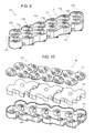
- figure 14 shows a modular array of twenty-four sinuous slot elements realized using two "twelve-sinuous-slot-elements arrays", in particular two antenna systems 70 in which no changes in inter-distances between elements and no modifications of the mechanics (i.e., of the hollow metallic structure 73) have been introduced.
- a second preferred embodiment of the present invention relates to an antenna system which differs from the antenna system 70 according to the first preferred embodiment only in the sinuous slot antenna array.
- the sinuous slot structures of sinuous slot antennas arranged along one and the same row are connected.
- figure 15 shows a sinuous slot antenna array 80 of an antenna system according to the second preferred embodiment of the present invention, said sinuous slot antenna array 80 comprising two rows of six sinuous slot antennas 81 each having a respective sinuous slot structure 82 with two sinuous slots (similar to the sinuous slot structure 30 previously described).
- the sinuous slot structure 82 of each sinuous slot antenna 81 having two adjacent sinuous slot antennas 81 along one and the same row has:
- each single sinuous slot antenna 81 is loaded with the surrounding ones, the total electrical length of the antenna grows significantly and, thence, the minimum operating frequency lowers.
- figure 16 the average gain of single element of the antenna system 70 at boresight versus frequency is shown.
- the graph shown in figure 16 has been calculated measuring all twelve elements pattern once at time with the other elements loaded to 50 Ohm. Then, by means of post-processing, the element average gain at boresight has been obtained.
- FIG 17 the scan losses of the antenna system 70 at four particular steering points versus frequency are shown.
- the curves shown in figure 17 represent the "losses" of array gain at the previously listed steering points compared to boresight.
Landscapes
- Variable-Direction Aerials And Aerial Arrays (AREA)
Claims (12)
- Antennensystem (70) für elektronische Gegenmaßnahmen, eine flach-Gruppenantenne (71; 80) aus drei oder mehr gewundenen Schlitzantennen (712; 81) aufweisend, die ein dreieckiges Gruppen-Gitter bildend angeordnet sind; wobei die Flach-Gruppenantenne (71; 80) einen geschlossenen Umfangsrand hat; wobei jede gewundene Schlitzantenne (712; 81) über eine jeweilige Speisestruktur (41) verfügt, die an einer unteren Fläche (713) der Flach-Gruppenantenne (71; 80) angeordnet ist;
wobei das Antennensystem (70) darüber hinaus eine hohle metallische Struktur (73) aufweist, die verfügt über:• eine Basis (732) mit einem geschlossenen Umfangsrand,• eine geschlossene Seitenwand (733), die sich vom geschlossenen Umfangsrand der Basis (732) bis zu einer vorgegebenen Höhe (H) erhebt, in der die geschlossene Seitenwand (733) mit einem geschlossenen oberen Rand endet; und• einen Hohlraum (731), der durch die Basis (732) und die geschlossene Seitenwand (733) bestimmt ist;wobei der Hohlraum (731) oben durch die Flach-Gruppenantenne (71; 80) geschlossen ist, deren geschlossener Umfangsrand auf/an dem geschlossenen oberen Rand der hohlen metallischen Struktur (73) befestigt ist, und deren Bodenfläche (713) dem Hohlraum (731) zugewandt ist;
wobei das Antennensystem (70) darüber hinaus einen Schaumstoffabstandhalter (72) aufweist, der den Hohlraum (731) füllt und die gewundenen Schlitzantennen (712; 81) von der Basis (732) mit der vorgegebenen Höhe (H) beabstandet hält;
wobei die vorgegebene Höhe (H) gleich einem Viertel einer Wellenlänge ist, die einer mittleren Betriebsfrequenz der Antennengruppe (71; 80) entspricht;
wobei eine absorbierende Schicht die Basis (732) am Boden des Hohlraums (731) bedeckt, wobei die absorbierende Schicht dazu konzipiert ist, Oberflächenströme an der Basis (732) am Boden des Hohlraums (731) zu absorbieren;
und wobei für jede gewundene Schlitzantenne (712; 81) die hohle metallische Struktur (73) darüber hinaus über ein entsprechendes Speisetürmchen (735) verfügt, das von der Basis (732) durch die absorbierende Schicht und den Schaumstoffabstandhalter (72) in den Hohlraum (731) bis zur Speisestruktur (41) der gewundenen Schlitzantenne (712; 81) vorragt, und der mit der Speisestruktur (41) der gewundenen Schlitzantenne (712; 81) verbunden ist;
wobei das Antennensystem (70) dadurch gekennzeichnet ist, dass für jede gewundene Schlitzantenne (712; 81) die hohle metallische Struktur (73) darüber hinaus über ein entsprechendes reflektierendes, sich verjüngendes Element (734) verfügt, das von der Basis (732) durch die absorbierende Schicht und den Schaumstoffabstandhalter (72) in den Hohlraum (731) vorragt, unter der gewundenen Schlitzantenne (712; 81) angeordnet und dazu konzipiert ist, eine Rückstrahlung von der gewundenen Schlitzantenne (712; 81) zu reflektieren. - Antennensystem nach Anspruch 1, wobei das dreieckigen Gruppen-Gitter zwei oder mehr Reihen aus gewundenen Schlitzantennen (712; 81) aufweist;
wobei benachbarte gewundene Schlitzantennen (712; 81) in ein und derselben Reihe um einen ersten Abstand voneinander beabstandet sind, der gleich drei Hälften einer Wellenlänge ist, die der niedrigsten Betriebsfrequenz der Gruppenantenne (71; 80) entspricht;
und wobei benachbarte Reihen um einen zweiten Abstand voneinander beabstandet sind, der gleich sieben Sechstel der Wellenlänge ist, die der niedrigsten Betriebsfrequenz der Gruppenantenne (71; 80) entspricht. - Antennensystem nach Anspruch 1 oder 2, wobei die Flach-Gruppenantenne (71; 80) über eine dielektrische Schicht mit einer Oberseite (711) und einer Unterseite (713) verfügt;
wobei die Oberseite (711) der dielektrischen Schicht metallisiert ist;
wobei jede gewundene Schlitzantenne (712; 81) in einem jeweiligen Teilbereich der dielektrischen Schicht hergestellt ist;
und wobei die Speisestrukturen (41) der gewundenen Schlitzantennen (712; 81) auf der Unterseite (713) der dielektrischen Schicht ausgebildet sind. - Antennensystem nach einem der vorhergehenden Ansprüche, wobei die Speisestruktur (41) jeder gewundenen Schlitzantenne (712; 81) über einen Endabschnitt verfügt, der zu einem 90°-Funkfrequenzübergang konzipiert ist;
und wobei jedes Speisetürmchen (735) über einen Verbindungsabschnitt verfügt, der zu einem 90°-Funkfrequenzübergang konzipiert ist, und der mit dem Endabschnitt der Speisestruktur (41) der entsprechenden gewundenen Schlitzantenne (712; 81) gekoppelt ist. - Antennensystem nach einem der vorhergehenden Ansprüche, wobei jede gewundene Schlitzantenne (712) über eine jeweilige gewundene Schlitzstruktur (30) verfügt; und wobei die gewundene Schlitzstruktur (30) von verschiedenen gewundenen Schlitzantennen (712) nicht verbunden sind.
- Antennensystem nach einem der Ansprüche 1 bis 4, wobei jede gewundene Schlitzantenne (81) über eine jeweilige gewundene Schlitzstruktur (82) verfügt;
wobei das dreieckige Gruppen-Gitter zwei oder mehr Reihen aus gewundenen Schlitzantennen (81) aufweist;
und wobei die gewundenen Schlitzstrukturen (82) der gewundenen Schlitzantennen (81) in ein und derselben Reihe verbunden sind. - Antennensystem nach Anspruch 6, wobei die gewundene Schlitzstruktur (82) jeder gewundenen Schlitzantenne (81) über zwei gewundene Schlitze verfügt;
und wobei die gewundene Schlitzstruktur (82) jeder gewundenen Schlitzantenne (81) angrenzend an zwei gewundene Schlitzantennen (81) in ein und derselben Reihe:• die äußerste Zelle eines ihrer zwei gewundenen Schlitze an die äußerste Zelle eines gewundenen Schlitzes einer der zwei angrenzenden gewundenen Schlitzantennen (81) angeschlossen hat; und• die äußerste Zelle des anderen ihrer zwei gewundenen Schlitze an die äußerste Zelle eines gewundenen Schlitzes der anderen der zwei angrenzenden Schlitzantennen (81) angeschlossen hat. - Antennensystem nach einem der vorhergehenden Ansprüche, wobei es sich bei der Flach-Gruppenantenne (71; 80) um eine planare oder konforme Gruppenantenne handelt.
- Modulares Antennensystem, mehrere Antennensysteme (70) nach einem der vorhergehenden Ansprüche umfassend; wobei die Antennensysteme (70) nebeneinander angeordnet sind, wodurch eine modulare Antennenstruktur gebildet ist.
- Modulares Antennensystem nach Anspruch 9, wobei das Seitenprofil jedes Antennensystems (70) sinusförmig ist.
- Phasengesteuertes Gruppensystem für elektronische Gegenmaßnahmen, das Antennensystem (70) nach einem der Ansprüche 1 bis 8 oder das modulare Antennensystem nach Anspruch 9 oder 10 umfassend.
- System für elektronische Gegenmaßnahmen, das Antennensystem (70) nach einem der Ansprüche 1 bis 8 oder das modulare Antennensystem nach Anspruch 9 oder 10 umfassend.
Priority Applications (1)
| Application Number | Priority Date | Filing Date | Title |
|---|---|---|---|
| EP13155549.2A EP2629367B1 (de) | 2012-02-17 | 2013-02-15 | Flache wellenförmige Ultrabreitband-Schlitzantennengruppe |
Applications Claiming Priority (2)
| Application Number | Priority Date | Filing Date | Title |
|---|---|---|---|
| EP12425035 | 2012-02-17 | ||
| EP13155549.2A EP2629367B1 (de) | 2012-02-17 | 2013-02-15 | Flache wellenförmige Ultrabreitband-Schlitzantennengruppe |
Publications (2)
| Publication Number | Publication Date |
|---|---|
| EP2629367A1 EP2629367A1 (de) | 2013-08-21 |
| EP2629367B1 true EP2629367B1 (de) | 2016-01-13 |
Family
ID=47720423
Family Applications (1)
| Application Number | Title | Priority Date | Filing Date |
|---|---|---|---|
| EP13155549.2A Not-in-force EP2629367B1 (de) | 2012-02-17 | 2013-02-15 | Flache wellenförmige Ultrabreitband-Schlitzantennengruppe |
Country Status (5)
| Country | Link |
|---|---|
| EP (1) | EP2629367B1 (de) |
| BR (1) | BR102013003551A8 (de) |
| ES (1) | ES2566204T3 (de) |
| IL (1) | IL224742A (de) |
| SG (1) | SG193102A1 (de) |
Families Citing this family (9)
| Publication number | Priority date | Publication date | Assignee | Title |
|---|---|---|---|---|
| EP3041135A1 (de) | 2014-12-30 | 2016-07-06 | Elettronica S.p.A. | Aktives Balun und monolithische integrierte Mikrowellenschaltung damit, für ultrabreitbandigen Empfang |
| US9991605B2 (en) | 2015-06-16 | 2018-06-05 | The Mitre Corporation | Frequency-scaled ultra-wide spectrum element |
| US10056699B2 (en) | 2015-06-16 | 2018-08-21 | The Mitre Cooperation | Substrate-loaded frequency-scaled ultra-wide spectrum element |
| US10854993B2 (en) | 2017-09-18 | 2020-12-01 | The Mitre Corporation | Low-profile, wideband electronically scanned array for geo-location, communications, and radar |
| US20190097299A1 (en) * | 2017-09-22 | 2019-03-28 | Kymeta Corporation | Integrated transceiver for antenna systems |
| US10886625B2 (en) | 2018-08-28 | 2021-01-05 | The Mitre Corporation | Low-profile wideband antenna array configured to utilize efficient manufacturing processes |
| CN110658563B (zh) * | 2019-10-23 | 2021-09-28 | 中国工程物理研究院电子工程研究所 | 一种应用于毫米波人体安检系统的收发天线阵列 |
| CN112803173B (zh) * | 2021-04-15 | 2021-06-22 | 中航富士达科技股份有限公司 | 一种Ka波段双极化缝隙天线同轴馈电网络 |
| CN114122671A (zh) * | 2021-12-03 | 2022-03-01 | 国网辽宁省电力有限公司辽阳供电公司 | 应用于隔离刀闸的数据采集天线 |
Family Cites Families (3)
| Publication number | Priority date | Publication date | Assignee | Title |
|---|---|---|---|---|
| US4658262A (en) | 1985-02-19 | 1987-04-14 | Duhamel Raymond H | Dual polarized sinuous antennas |
| US6219006B1 (en) * | 1999-02-17 | 2001-04-17 | Ail Systems, Inc. | High efficiency broadband antenna |
| FR2925771B1 (fr) * | 2007-12-21 | 2010-02-26 | Thales Sa | Reseau d'antennes directives multi polarisations large bande |
-
2013
- 2013-02-14 IL IL224742A patent/IL224742A/en not_active IP Right Cessation
- 2013-02-15 SG SG2013011655A patent/SG193102A1/en unknown
- 2013-02-15 ES ES13155549.2T patent/ES2566204T3/es active Active
- 2013-02-15 EP EP13155549.2A patent/EP2629367B1/de not_active Not-in-force
- 2013-02-15 BR BR102013003551A patent/BR102013003551A8/pt not_active IP Right Cessation
Also Published As
| Publication number | Publication date |
|---|---|
| IL224742A (en) | 2017-01-31 |
| IL224742A0 (en) | 2013-06-27 |
| SG193102A1 (en) | 2013-09-30 |
| EP2629367A1 (de) | 2013-08-21 |
| BR102013003551A8 (pt) | 2015-11-24 |
| BR102013003551A2 (pt) | 2015-09-08 |
| ES2566204T3 (es) | 2016-04-11 |
Similar Documents
| Publication | Publication Date | Title |
|---|---|---|
| EP2629367B1 (de) | Flache wellenförmige Ultrabreitband-Schlitzantennengruppe | |
| US6642898B2 (en) | Fractal cross slot antenna | |
| EP2335316B1 (de) | Kompakte zirkularpolarisierte antenne mit erweiterter frequenzbandbreite | |
| EP1958290B1 (de) | Patch-antennenelement und seine anwendung in einer phasengesteuerten gruppenantenne | |
| US8354972B2 (en) | Dual-polarized radiating element, dual-band dual-polarized antenna assembly and dual-polarized antenna array | |
| EP0345454B1 (de) | Streifenleiter Array-Antenne | |
| US10862210B2 (en) | Multiple band polarization rotating phased array element | |
| ES2314295T3 (es) | Antena miniatura que tiene una estructura volumetrica. | |
| US10978812B2 (en) | Single layer shared aperture dual band antenna | |
| US9413073B2 (en) | Augmented E-plane taper techniques in variable inclination continuous transverse (VICTS) antennas | |
| US20230378662A1 (en) | Uwb vivaldi array antenna | |
| Edalati et al. | Wideband reflectarray antenna based on miniaturized element frequency selective surfaces | |
| US20210151873A1 (en) | Wideband dual polarized antenna array system | |
| Kedar et al. | Wide beam tapered slot antenna for wide angle scanning phased array antenna | |
| CN105900281B (zh) | 圆极化标量阻抗人工阻抗表面天线 | |
| KR101803208B1 (ko) | 단일 방사체 다중 급전을 이용한 빔조향 안테나 | |
| CN216120772U (zh) | 一种圆极化psoam阵列天线、无线通信系统 | |
| Miura et al. | A high-efficiency circularly-polarized aperture array antenna with a corporate-feed circuit in the 60 GHz band | |
| Li et al. | Compact, low-profile, HIS-based pattern-reconfigurable antenna for wide-angle scanning | |
| Ali et al. | Enhanced high gain planar endfire dipole antenna using third higher order | |
| Wang et al. | Two-dimensional image theory-based surface-mounted linear array with azimuth wide-angle scanning performance | |
| US9748640B2 (en) | Helix-loaded meandered loxodromic spiral antenna | |
| Ali et al. | A Modular Conformal Antenna Array for Wide-Beam SAR and DAA Radars | |
| Prasad et al. | Lightweight ultra-wideband antenna array equipped with thin frequency selective surface for high-gain applications | |
| Wang et al. | A electronically steerable radiator and reflector array antenna based on Three-Dimensional Frequency Selective Structure |
Legal Events
| Date | Code | Title | Description |
|---|---|---|---|
| PUAI | Public reference made under article 153(3) epc to a published international application that has entered the european phase |
Free format text: ORIGINAL CODE: 0009012 |
|
| AK | Designated contracting states |
Kind code of ref document: A1 Designated state(s): AL AT BE BG CH CY CZ DE DK EE ES FI FR GB GR HR HU IE IS IT LI LT LU LV MC MK MT NL NO PL PT RO RS SE SI SK SM TR |
|
| AX | Request for extension of the european patent |
Extension state: BA ME |
|
| 17P | Request for examination filed |
Effective date: 20140221 |
|
| RBV | Designated contracting states (corrected) |
Designated state(s): AL AT BE BG CH CY CZ DE DK EE ES FI FR GB GR HR HU IE IS IT LI LT LU LV MC MK MT NL NO PL PT RO RS SE SI SK SM TR |
|
| GRAP | Despatch of communication of intention to grant a patent |
Free format text: ORIGINAL CODE: EPIDOSNIGR1 |
|
| INTG | Intention to grant announced |
Effective date: 20150717 |
|
| GRAS | Grant fee paid |
Free format text: ORIGINAL CODE: EPIDOSNIGR3 |
|
| GRAA | (expected) grant |
Free format text: ORIGINAL CODE: 0009210 |
|
| AK | Designated contracting states |
Kind code of ref document: B1 Designated state(s): AL AT BE BG CH CY CZ DE DK EE ES FI FR GB GR HR HU IE IS IT LI LT LU LV MC MK MT NL NO PL PT RO RS SE SI SK SM TR |
|
| REG | Reference to a national code |
Ref country code: GB Ref legal event code: FG4D |
|
| REG | Reference to a national code |
Ref country code: CH Ref legal event code: EP |
|
| REG | Reference to a national code |
Ref country code: IE Ref legal event code: FG4D |
|
| REG | Reference to a national code |
Ref country code: AT Ref legal event code: REF Ref document number: 771055 Country of ref document: AT Kind code of ref document: T Effective date: 20160215 |
|
| REG | Reference to a national code |
Ref country code: DE Ref legal event code: R096 Ref document number: 602013004555 Country of ref document: DE |
|
| REG | Reference to a national code |
Ref country code: ES Ref legal event code: FG2A Ref document number: 2566204 Country of ref document: ES Kind code of ref document: T3 Effective date: 20160411 |
|
| REG | Reference to a national code |
Ref country code: SE Ref legal event code: TRGR |
|
| REG | Reference to a national code |
Ref country code: LT Ref legal event code: MG4D |
|
| REG | Reference to a national code |
Ref country code: NL Ref legal event code: MP Effective date: 20160113 |
|
| PG25 | Lapsed in a contracting state [announced via postgrant information from national office to epo] |
Ref country code: BE Free format text: LAPSE BECAUSE OF NON-PAYMENT OF DUE FEES Effective date: 20160229 |
|
| REG | Reference to a national code |
Ref country code: AT Ref legal event code: MK05 Ref document number: 771055 Country of ref document: AT Kind code of ref document: T Effective date: 20160113 |
|
| PG25 | Lapsed in a contracting state [announced via postgrant information from national office to epo] |
Ref country code: NL Free format text: LAPSE BECAUSE OF FAILURE TO SUBMIT A TRANSLATION OF THE DESCRIPTION OR TO PAY THE FEE WITHIN THE PRESCRIBED TIME-LIMIT Effective date: 20160113 |
|
| PG25 | Lapsed in a contracting state [announced via postgrant information from national office to epo] |
Ref country code: GR Free format text: LAPSE BECAUSE OF FAILURE TO SUBMIT A TRANSLATION OF THE DESCRIPTION OR TO PAY THE FEE WITHIN THE PRESCRIBED TIME-LIMIT Effective date: 20160414 Ref country code: NO Free format text: LAPSE BECAUSE OF FAILURE TO SUBMIT A TRANSLATION OF THE DESCRIPTION OR TO PAY THE FEE WITHIN THE PRESCRIBED TIME-LIMIT Effective date: 20160413 Ref country code: HR Free format text: LAPSE BECAUSE OF FAILURE TO SUBMIT A TRANSLATION OF THE DESCRIPTION OR TO PAY THE FEE WITHIN THE PRESCRIBED TIME-LIMIT Effective date: 20160113 |
|
| PG25 | Lapsed in a contracting state [announced via postgrant information from national office to epo] |
Ref country code: PL Free format text: LAPSE BECAUSE OF FAILURE TO SUBMIT A TRANSLATION OF THE DESCRIPTION OR TO PAY THE FEE WITHIN THE PRESCRIBED TIME-LIMIT Effective date: 20160113 Ref country code: PT Free format text: LAPSE BECAUSE OF FAILURE TO SUBMIT A TRANSLATION OF THE DESCRIPTION OR TO PAY THE FEE WITHIN THE PRESCRIBED TIME-LIMIT Effective date: 20160513 Ref country code: AT Free format text: LAPSE BECAUSE OF FAILURE TO SUBMIT A TRANSLATION OF THE DESCRIPTION OR TO PAY THE FEE WITHIN THE PRESCRIBED TIME-LIMIT Effective date: 20160113 Ref country code: IS Free format text: LAPSE BECAUSE OF FAILURE TO SUBMIT A TRANSLATION OF THE DESCRIPTION OR TO PAY THE FEE WITHIN THE PRESCRIBED TIME-LIMIT Effective date: 20160513 Ref country code: LV Free format text: LAPSE BECAUSE OF FAILURE TO SUBMIT A TRANSLATION OF THE DESCRIPTION OR TO PAY THE FEE WITHIN THE PRESCRIBED TIME-LIMIT Effective date: 20160113 Ref country code: RS Free format text: LAPSE BECAUSE OF FAILURE TO SUBMIT A TRANSLATION OF THE DESCRIPTION OR TO PAY THE FEE WITHIN THE PRESCRIBED TIME-LIMIT Effective date: 20160113 Ref country code: LT Free format text: LAPSE BECAUSE OF FAILURE TO SUBMIT A TRANSLATION OF THE DESCRIPTION OR TO PAY THE FEE WITHIN THE PRESCRIBED TIME-LIMIT Effective date: 20160113 |
|
| REG | Reference to a national code |
Ref country code: CH Ref legal event code: PL |
|
| REG | Reference to a national code |
Ref country code: DE Ref legal event code: R097 Ref document number: 602013004555 Country of ref document: DE |
|
| PG25 | Lapsed in a contracting state [announced via postgrant information from national office to epo] |
Ref country code: DK Free format text: LAPSE BECAUSE OF FAILURE TO SUBMIT A TRANSLATION OF THE DESCRIPTION OR TO PAY THE FEE WITHIN THE PRESCRIBED TIME-LIMIT Effective date: 20160113 Ref country code: CH Free format text: LAPSE BECAUSE OF NON-PAYMENT OF DUE FEES Effective date: 20160229 Ref country code: MC Free format text: LAPSE BECAUSE OF FAILURE TO SUBMIT A TRANSLATION OF THE DESCRIPTION OR TO PAY THE FEE WITHIN THE PRESCRIBED TIME-LIMIT Effective date: 20160113 Ref country code: LI Free format text: LAPSE BECAUSE OF NON-PAYMENT OF DUE FEES Effective date: 20160229 Ref country code: EE Free format text: LAPSE BECAUSE OF FAILURE TO SUBMIT A TRANSLATION OF THE DESCRIPTION OR TO PAY THE FEE WITHIN THE PRESCRIBED TIME-LIMIT Effective date: 20160113 |
|
| PLBE | No opposition filed within time limit |
Free format text: ORIGINAL CODE: 0009261 |
|
| STAA | Information on the status of an ep patent application or granted ep patent |
Free format text: STATUS: NO OPPOSITION FILED WITHIN TIME LIMIT |
|
| REG | Reference to a national code |
Ref country code: FR Ref legal event code: ST Effective date: 20161028 |
|
| PG25 | Lapsed in a contracting state [announced via postgrant information from national office to epo] |
Ref country code: CZ Free format text: LAPSE BECAUSE OF FAILURE TO SUBMIT A TRANSLATION OF THE DESCRIPTION OR TO PAY THE FEE WITHIN THE PRESCRIBED TIME-LIMIT Effective date: 20160113 Ref country code: SM Free format text: LAPSE BECAUSE OF FAILURE TO SUBMIT A TRANSLATION OF THE DESCRIPTION OR TO PAY THE FEE WITHIN THE PRESCRIBED TIME-LIMIT Effective date: 20160113 Ref country code: RO Free format text: LAPSE BECAUSE OF FAILURE TO SUBMIT A TRANSLATION OF THE DESCRIPTION OR TO PAY THE FEE WITHIN THE PRESCRIBED TIME-LIMIT Effective date: 20160113 Ref country code: SK Free format text: LAPSE BECAUSE OF FAILURE TO SUBMIT A TRANSLATION OF THE DESCRIPTION OR TO PAY THE FEE WITHIN THE PRESCRIBED TIME-LIMIT Effective date: 20160113 |
|
| REG | Reference to a national code |
Ref country code: IE Ref legal event code: MM4A |
|
| 26N | No opposition filed |
Effective date: 20161014 |
|
| PG25 | Lapsed in a contracting state [announced via postgrant information from national office to epo] |
Ref country code: BE Free format text: LAPSE BECAUSE OF FAILURE TO SUBMIT A TRANSLATION OF THE DESCRIPTION OR TO PAY THE FEE WITHIN THE PRESCRIBED TIME-LIMIT Effective date: 20160113 |
|
| PG25 | Lapsed in a contracting state [announced via postgrant information from national office to epo] |
Ref country code: FR Free format text: LAPSE BECAUSE OF NON-PAYMENT OF DUE FEES Effective date: 20160314 Ref country code: IE Free format text: LAPSE BECAUSE OF NON-PAYMENT OF DUE FEES Effective date: 20160215 |
|
| PG25 | Lapsed in a contracting state [announced via postgrant information from national office to epo] |
Ref country code: BG Free format text: LAPSE BECAUSE OF FAILURE TO SUBMIT A TRANSLATION OF THE DESCRIPTION OR TO PAY THE FEE WITHIN THE PRESCRIBED TIME-LIMIT Effective date: 20160413 Ref country code: SI Free format text: LAPSE BECAUSE OF FAILURE TO SUBMIT A TRANSLATION OF THE DESCRIPTION OR TO PAY THE FEE WITHIN THE PRESCRIBED TIME-LIMIT Effective date: 20160113 |
|
| PG25 | Lapsed in a contracting state [announced via postgrant information from national office to epo] |
Ref country code: MT Free format text: LAPSE BECAUSE OF FAILURE TO SUBMIT A TRANSLATION OF THE DESCRIPTION OR TO PAY THE FEE WITHIN THE PRESCRIBED TIME-LIMIT Effective date: 20160113 |
|
| PGFP | Annual fee paid to national office [announced via postgrant information from national office to epo] |
Ref country code: ES Payment date: 20180322 Year of fee payment: 6 Ref country code: FI Payment date: 20180221 Year of fee payment: 6 Ref country code: GB Payment date: 20180227 Year of fee payment: 6 |
|
| PG25 | Lapsed in a contracting state [announced via postgrant information from national office to epo] |
Ref country code: HU Free format text: LAPSE BECAUSE OF FAILURE TO SUBMIT A TRANSLATION OF THE DESCRIPTION OR TO PAY THE FEE WITHIN THE PRESCRIBED TIME-LIMIT; INVALID AB INITIO Effective date: 20130215 Ref country code: CY Free format text: LAPSE BECAUSE OF FAILURE TO SUBMIT A TRANSLATION OF THE DESCRIPTION OR TO PAY THE FEE WITHIN THE PRESCRIBED TIME-LIMIT Effective date: 20160113 |
|
| PGFP | Annual fee paid to national office [announced via postgrant information from national office to epo] |
Ref country code: IT Payment date: 20180205 Year of fee payment: 6 Ref country code: SE Payment date: 20180227 Year of fee payment: 6 Ref country code: TR Payment date: 20180202 Year of fee payment: 6 |
|
| PG25 | Lapsed in a contracting state [announced via postgrant information from national office to epo] |
Ref country code: MT Free format text: LAPSE BECAUSE OF FAILURE TO SUBMIT A TRANSLATION OF THE DESCRIPTION OR TO PAY THE FEE WITHIN THE PRESCRIBED TIME-LIMIT Effective date: 20160229 Ref country code: MK Free format text: LAPSE BECAUSE OF FAILURE TO SUBMIT A TRANSLATION OF THE DESCRIPTION OR TO PAY THE FEE WITHIN THE PRESCRIBED TIME-LIMIT Effective date: 20160113 Ref country code: LU Free format text: LAPSE BECAUSE OF NON-PAYMENT OF DUE FEES Effective date: 20160215 |
|
| PGFP | Annual fee paid to national office [announced via postgrant information from national office to epo] |
Ref country code: DE Payment date: 20180430 Year of fee payment: 6 |
|
| PG25 | Lapsed in a contracting state [announced via postgrant information from national office to epo] |
Ref country code: AL Free format text: LAPSE BECAUSE OF FAILURE TO SUBMIT A TRANSLATION OF THE DESCRIPTION OR TO PAY THE FEE WITHIN THE PRESCRIBED TIME-LIMIT Effective date: 20160113 |
|
| REG | Reference to a national code |
Ref country code: DE Ref legal event code: R119 Ref document number: 602013004555 Country of ref document: DE |
|
| REG | Reference to a national code |
Ref country code: SE Ref legal event code: EUG |
|
| GBPC | Gb: european patent ceased through non-payment of renewal fee |
Effective date: 20190215 |
|
| PG25 | Lapsed in a contracting state [announced via postgrant information from national office to epo] |
Ref country code: FI Free format text: LAPSE BECAUSE OF NON-PAYMENT OF DUE FEES Effective date: 20190215 Ref country code: SE Free format text: LAPSE BECAUSE OF NON-PAYMENT OF DUE FEES Effective date: 20190216 |
|
| PG25 | Lapsed in a contracting state [announced via postgrant information from national office to epo] |
Ref country code: DE Free format text: LAPSE BECAUSE OF NON-PAYMENT OF DUE FEES Effective date: 20190903 Ref country code: GB Free format text: LAPSE BECAUSE OF NON-PAYMENT OF DUE FEES Effective date: 20190215 |
|
| PG25 | Lapsed in a contracting state [announced via postgrant information from national office to epo] |
Ref country code: IT Free format text: LAPSE BECAUSE OF NON-PAYMENT OF DUE FEES Effective date: 20190215 |
|
| REG | Reference to a national code |
Ref country code: ES Ref legal event code: FD2A Effective date: 20200330 |
|
| PG25 | Lapsed in a contracting state [announced via postgrant information from national office to epo] |
Ref country code: ES Free format text: LAPSE BECAUSE OF NON-PAYMENT OF DUE FEES Effective date: 20190216 |
|
| PG25 | Lapsed in a contracting state [announced via postgrant information from national office to epo] |
Ref country code: TR Free format text: LAPSE BECAUSE OF NON-PAYMENT OF DUE FEES Effective date: 20190215 |