EP2629549B1 - Ultraschallwandler und ultraschalldiagnosevorrichtung damit - Google Patents
Ultraschallwandler und ultraschalldiagnosevorrichtung damit Download PDFInfo
- Publication number
- EP2629549B1 EP2629549B1 EP11832603.2A EP11832603A EP2629549B1 EP 2629549 B1 EP2629549 B1 EP 2629549B1 EP 11832603 A EP11832603 A EP 11832603A EP 2629549 B1 EP2629549 B1 EP 2629549B1
- Authority
- EP
- European Patent Office
- Prior art keywords
- insulating film
- projections
- hollow portion
- membrane
- ultrasonic transducer
- Prior art date
- Legal status (The legal status is an assumption and is not a legal conclusion. Google has not performed a legal analysis and makes no representation as to the accuracy of the status listed.)
- Active
Links
Images



Classifications
-
- H—ELECTRICITY
- H04—ELECTRIC COMMUNICATION TECHNIQUE
- H04R—LOUDSPEAKERS, MICROPHONES, GRAMOPHONE PICK-UPS OR LIKE ACOUSTIC ELECTROMECHANICAL TRANSDUCERS; ELECTRIC HEARING AIDS; PUBLIC ADDRESS SYSTEMS
- H04R19/00—Electrostatic transducers
-
- A—HUMAN NECESSITIES
- A61—MEDICAL OR VETERINARY SCIENCE; HYGIENE
- A61B—DIAGNOSIS; SURGERY; IDENTIFICATION
- A61B8/00—Diagnosis using ultrasonic, sonic or infrasonic waves
- A61B8/44—Constructional features of the ultrasonic, sonic or infrasonic diagnostic device
- A61B8/4483—Constructional features of the ultrasonic, sonic or infrasonic diagnostic device characterised by features of the ultrasound transducer
-
- H—ELECTRICITY
- H02—GENERATION; CONVERSION OR DISTRIBUTION OF ELECTRIC POWER
- H02N—ELECTRIC MACHINES NOT OTHERWISE PROVIDED FOR
- H02N1/00—Electrostatic generators or motors using a solid moving electrostatic charge carrier
- H02N1/06—Influence generators
- H02N1/08—Influence generators with conductive charge carrier, i.e. capacitor machines
-
- A—HUMAN NECESSITIES
- A61—MEDICAL OR VETERINARY SCIENCE; HYGIENE
- A61B—DIAGNOSIS; SURGERY; IDENTIFICATION
- A61B8/00—Diagnosis using ultrasonic, sonic or infrasonic waves
-
- A—HUMAN NECESSITIES
- A61—MEDICAL OR VETERINARY SCIENCE; HYGIENE
- A61B—DIAGNOSIS; SURGERY; IDENTIFICATION
- A61B8/00—Diagnosis using ultrasonic, sonic or infrasonic waves
- A61B8/44—Constructional features of the ultrasonic, sonic or infrasonic diagnostic device
- A61B8/4483—Constructional features of the ultrasonic, sonic or infrasonic diagnostic device characterised by features of the ultrasound transducer
- A61B8/4494—Constructional features of the ultrasonic, sonic or infrasonic diagnostic device characterised by features of the ultrasound transducer characterised by the arrangement of the transducer elements
-
- B—PERFORMING OPERATIONS; TRANSPORTING
- B06—GENERATING OR TRANSMITTING MECHANICAL VIBRATIONS IN GENERAL
- B06B—METHODS OR APPARATUS FOR GENERATING OR TRANSMITTING MECHANICAL VIBRATIONS OF INFRASONIC, SONIC, OR ULTRASONIC FREQUENCY, e.g. FOR PERFORMING MECHANICAL WORK IN GENERAL
- B06B1/00—Methods or apparatus for generating mechanical vibrations of infrasonic, sonic, or ultrasonic frequency
- B06B1/02—Methods or apparatus for generating mechanical vibrations of infrasonic, sonic, or ultrasonic frequency making use of electrical energy
- B06B1/0292—Electrostatic transducers, e.g. electret-type
-
- G—PHYSICS
- G01—MEASURING; TESTING
- G01N—INVESTIGATING OR ANALYSING MATERIALS BY DETERMINING THEIR CHEMICAL OR PHYSICAL PROPERTIES
- G01N29/00—Investigating or analysing materials by the use of ultrasonic, sonic or infrasonic waves; Visualisation of the interior of objects by transmitting ultrasonic or sonic waves through the object
- G01N29/22—Details, e.g. general constructional or apparatus details
- G01N29/24—Probes
-
- G—PHYSICS
- G01—MEASURING; TESTING
- G01N—INVESTIGATING OR ANALYSING MATERIALS BY DETERMINING THEIR CHEMICAL OR PHYSICAL PROPERTIES
- G01N29/00—Investigating or analysing materials by the use of ultrasonic, sonic or infrasonic waves; Visualisation of the interior of objects by transmitting ultrasonic or sonic waves through the object
- G01N29/22—Details, e.g. general constructional or apparatus details
- G01N29/24—Probes
- G01N29/2406—Electrostatic or capacitive probes, e.g. electret or cMUT-probes
-
- H—ELECTRICITY
- H04—ELECTRIC COMMUNICATION TECHNIQUE
- H04R—LOUDSPEAKERS, MICROPHONES, GRAMOPHONE PICK-UPS OR LIKE ACOUSTIC ELECTROMECHANICAL TRANSDUCERS; ELECTRIC HEARING AIDS; PUBLIC ADDRESS SYSTEMS
- H04R19/00—Electrostatic transducers
- H04R19/04—Microphones
Definitions
- the present invention relates to an ultrasonic transducer and an ultrasonic diagnostic equipment using the ultrasonic transducer. More particularly, the present invention is concerned with an ultrasonic transducer manufactured using a micro-electro-mechanical systems (MEMS) technology.
- MEMS micro-electro-mechanical systems
- Ultrasonic transducers that transmit or receive an ultrasonic wave are employed in diagnosis of a tumor or the like in a human body, nondestructive testing of a structure, sensing of the velocity of a fluid, or the like.
- CMUT capacitive micromachined ultrasonic transducer
- patent literature 1 patent literature 2, and patent literature 3 have disclosed improvement of reliability in activities of a CMUT.
- Patent literature 4 has disclosed a method of controlling a center frequency and a bandwidth offered by the CMUT.
- the patent literature 1 has disclosed a structure in which: projections of an insulating film jutting out to a hollow portion of a CMUT are formed; and even when a direct-current (dc) voltage or alternating-current (ac) voltage equal to or higher than a collapse voltage is applied, although the projection undersurfaces come into contact with the hollow portion bottom, a membrane undersurface does not come into contact with the hollow portion bottom.
- dc direct-current
- ac alternating-current
- the patent literature 2 describes a structure in which portions of an electrode are pierced for fear fields in which a membrane undersurface comes into contact with a hollow portion bottom may be sandwiched between upper and lower electrodes.
- the structure since the electric field strength in a membrane insulating film in the contact fields is decreased, charge injection can be avoided.
- the area of layered portions of the upper and lower electrodes diminishes accordingly. This invites a rise in a driving voltage for a CMUT or degradation in receiving sensitivity.
- a membrane is provided with rigid members in order to adjust the rigidness of the entire membrane.
- the center frequency and bandwidth offered by a CMUT are controlled.
- introduction of the rigid members brings about a rise in a driving voltage. How to ensure reliability in device activities becomes an object to be accomplished.
- an object of the present invention is to provide an ultrasonic transducer which is a CMUT that has projections jutted out to a hollow portion and has at least one of an upper electrode and lower electrode located at a position at which the electrode is not layered over the projections when viewed from the upper surface, and an ultrasonic diagnostic equipment employing the CMUT.
- a voltage margin between the instant projection undersurfaces come into contact with a hollow portion bottom and the instant a membrane undersurface comes into contact with the hollow portion bottom is preserved, charge injection into a membrane insulating film is suppressed, and a high transmission sound pressure and a highly reliable structure are realized.
- an ultrasonic transducer of the present invention includes a lower electrode, a hollow portion formed over the lower electrode and enclosed with an insulating film, an upper electrode formed over the hollow portion, and plural projections of the insulating film formed in the hollow portion, according to the preamble of independent claim 1.
- the ultrasonic transducer has plural rigid members formed over the hollow portion according to the characterising portion of claim 1.
- the rigid members are beam members.
- a membrane including the insulating film, upper electrode, and beam members may have a portion thereof, in which the beam members are disposed, made thicker than a portion thereof, in which the beam members are not disposed, by the thickness of the beam members.
- the ultrasonic transducer of the present invention includes an upper insulating film formed to cover the upper electrode and hollow portion.
- the beam members may be disposed over the upper insulating film.
- the ultrasonic transducer of the present invention includes an upper insulating film formed to cover the upper electrode and hollow portion.
- the beam members may be embedded in the upper insulating film.
- the rigid members may be members exhibiting a higher Young's modulus than the membrane, which includes the insulating film, upper electrode, and beam members, does.
- the ultrasonic transducer of the present invention includes an upper insulating film formed to cover the upper electrode and hollow portion.
- the members of the higher Young's modulus may be embedded in the upper insulating film.
- the members of the higher Young's modulus may be formed by embedding a metallic material such as tungsten or a ceramic material such as alumina.
- the members of the higher Young's modulus may be formed by reforming the upper insulating film through ion implantation.
- the rigid members may be disposed so that the centers thereof coincide with the centers of the projections of the insulating film when viewed from the upper surface.
- the rigid members may be disposed so that one rigid member is layered over plural projections of the insulating film.
- the projections of the insulating film may be disposed over the top of the hollow portion.
- the projections of the insulating film may be disposed over the bottom of the hollow portion.
- the plural projections of the insulating film and the plural rigid members may be equidistantly disposed when viewed from the upper surface.
- the hollow portion may be circular or polygonal when viewed from the upper surface.
- the projections of the insulating film may be circular or polygonal when viewed from the upper surface.
- An ultrasonic diagnostic equipment of the present invention includes any of the foregoing ultrasonic transducers and a bias unit.
- CMUT capacitive micromachined ultrasonic transducer
- CMUT capacitive micromachined ultrasonic transducer
- a hollow portion 102 enclosed with an insulating film 103 is formed in an upper layer of a lower electrode 101.
- An upper electrode 104 is disposed over the hollow portion 102 with the insulating film 103 between them.
- electrostatic force works between the upper electrode 104 and lower electrode 101.
- a membrane 105 including the insulating film 103 and upper electrode 104 over the hollow portion 102 is vibrated at the frequency of the applied ac voltage, whereby an ultrasonic wave is originated.
- the membrane 105 For receiving, when the dc voltage alone is applied between the upper electrode 104 and lower electrode 101, the membrane 105 is vibrated due to the pressure of an ultrasonic wave having reached the surface of the membrane 105. This causes the distance between the upper electrode 104 and lower electrode 101 to vary. Eventually, the ultrasonic wave can be detected as a change in a capacitance.
- a signal-to-noise ratio is high.
- a capacitance change at a receiving time should be increased.
- the capacitance change may be increased by increasing the number of CMUTs or expanding the area of the CMUT. In this case, the size of the transducer gets larger. Therefore, it is necessary to increase the capacitance change per unit area. In other words, it is necessary to improve receiving sensitivity. Otherwise, by increasing a transmission sound pressure so as to raise a sound pressure of ultrasonic waves reflected from an object of inspection, the capacitance change at the receiving time can be increased.
- the spacing between the upper electrode 104 and lower electrode 101 should be narrowed as greatly as possible. Therefore, it is necessary to apply the highest possible dc voltage.
- an equivalent in vacuum of a magnitude of a deformation of the membrane corresponds to a distance equal to or larger than a one-third of the distance between the electrodes, an electrostatic force between the electrodes gets larger than a spring resilience of the membrane.
- a membrane undersurface 106 comes into contact with a hollow portion bottom 107. The voltage is called a collapse voltage. For these reasons, a dc voltage that is slightly lower than the collapse voltage is applied at the receiving time.
- the amplitude of the membrane should preferably be maximized.
- a driving condition for a CMUT has to be designated to such an extent that the membrane undersurface 106 does not come into contact with the hollow portion bottom 107.
- the driving condition is that the membrane should not come into contact with the bottom.
- the membrane is designed with a margin preserved, and the amplitude of the membrane is much smaller than the height of the hollow portion 102. Accordingly, the upper limit of the transmission sound pressure is restricted.
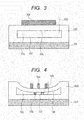
- Fig. 4 is a cross-sectional diagram showing a state in which projections 108 formed on the lower side of a membrane 105 are in contact with the hollow portion bottom 107. This state shall be called a projections-in-contact state.
- the amplitude of the membrane should preferably be maximized.
- a voltage equal to or higher than a voltage that brings about the projections-in-contact state is applied.
- the membrane 105 between the projections 108 deforms to approach the hollow portion bottom 107.
- the membrane 107 comes into contact with the hollow portion bottom 107 at a voltage equal to or higher than a certain voltage.
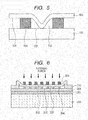
- This state shall be called a membrane-in-contact state, and is shown in Fig. 5 .
- charge injection to the membrane 105 takes place. Therefore, a key to improvement of activity reliability is to expand a voltage margin between the membrane-in-contact state and projections-in-contact state so as to avoid the membrane-in-contact state.
- the rigidness of the entire membrane should be upgraded. However, since a driving voltage is also raised, it is unacceptable. If the rigidness of the entire membrane observed with the projection undersurfaces 106 in non-contact with the hollow portion bottom 107 is not upgraded but the rigidness of the membrane in the projections-in-contact state is upgraded, the margin voltage can be expanded. The transmission sound pressure can be improved without the drift in the transmitting/receiving characteristic.
- the cross-sectional structure of a CMUT in accordance with the present embodiment will be described below in conjunction with Fig. 1 .
- the CMUT includes a parallelepiped lower electrode 201 disposed over a substrate 206, a parallelepiped hollow portion 202 disposed over the lower electrode 201, and a parallelepiped upper electrode 205 disposed over the hollow portion 202.
- An insulating film 209 is formed to cover the lower electrode 201 between the lower electrode 201 and hollow portion 202, and an insulating film 208 is formed to cover the hollow portion 202 and lower electrode 201 between the upper electrode 205 and hollow portion 202.
- At least one or more cylindrical projections 204 that jut out from the undersurface of the insulating film 208 to the hollow portion 202 are disposed.
- the insulating film 208 is coated with an insulating film 207.
- the foregoing projections 204 and the insulating films 207, 208, and 209 are made of a silicon oxide or silicon nitride.
- Over the top of the insulating film 207 at least one or more parallelepiped beam members that are rigid members 203 are disposed.
- the beam members that are the rigid members 203 may be, similarly to the insulating films 207, 208, and 209, made of the silicon oxide, silicon nitride, or the like, or may be made of another material.
- a membrane 210 including the insulating film 207, upper electrode 205, and insulating film 208 is vibrated, whereby an ultrasonic wave is transmitted.
- the surfaces of the projections 204 opposed to the insulating film 209 with the hollow portion between them shall be called projection undersurfaces 211, and the surface of the insulating film 209 exposed to the hollow portion shall be called a hollow portion bottom 213.
- the surface of the membrane 210 exposed to the hollow portion shall be called a membrane undersurface 212.
- projection contact an incident that the projection undersurfaces 211 come into contact with the hollow portion bottom 213 shall be called projection contact, and a voltage at that time shall be called a projection contact voltage.
- An incident that the membrane undersurface 212 comes into contact with the hollow portion bottom 213 shall be called membrane contact, and a voltage at that time shall be called a membrane contact voltage.
- a difference between the membrane contact voltage and projection contact voltage shall be called a margin voltage.
- a fabrication method for the CMUT shown in Fig. 1 will be described below.
- the fundamental fabrication method is described in the patent literature 3.
- a formation method for a beam member that is the rigid member 203 will be described below.
- the beam member is formed according to a photography technique and dry etching technique after a thin film which is a material of the beam member, for example, a silicon oxide or silicon nitride is deposited over the insulating film 207 according to a plasma chemical vapor deposition (CVD) method. Since the thickness of the membrane 210 largely affects a device characteristic, dry etching should be carefully performed for fear the insulating film 207 may get thinner.
- CVD plasma chemical vapor deposition
- the beam member that is the rigid member 203 is formed as a laminated film having the silicon nitride and silicon oxide layered in that order when viewed from the upper surface, and the insulating film 207 is made of the silicon nitride.
- a shaved volume of the insulating film 207, which serves as a bed, to be observed after etching the beam member that is the rigid member 203 is completed gets diminished, and a change in the thickness of the membrane 210 before and after the etching is performed can be suppressed.
- Fig. 2 is the top view of the structure shown in Fig. 1.
- Fig. 1 is a cross-sectional diagram showing a section cut along a line A-A' in Fig. 2 .
- the projections 204 or the like are seen through the rigid members 203.
- the hollow portion 202 and upper electrode 205 they shall have a width in the lengthwise direction of the sheet of paper and a lengths thereof in the sideways direction thereof.
- the rigid members 203 they shall have a length in the lengthwise direction of the sheet of paper and a width in the sideways direction thereof.
- the upper electrode 205 has plural circular holes.
- the respective projections 204 are disposed nearly in the center positions of the plural circular holes 214 of the upper electrode 205.
- the projections are located at positions at which the upper electrode 205 is not layered over the projections.
- the upper electrode 205 is absent from the vertical directions of the projections 204.
- the upper electrode 205 is partly pierced, and is disposed so that the upper electrode 205 is not layered over the projections 204 when viewed from the upper surface.
- the electrode to be pierced may be the lower electrode 201.
- the electrode to be pierced may be the lower electrode 201.
- at least one of the upper electrode 205 and lower electrode 201 should be located at a position at which the electrode is not layered over the projections 204 when viewed from the upper surface.
- the reason why the disposition is adopted is to increase an inter-electrode distance by piercing the electrode and thus decrease electric field strength for fear a strong electric field may be applied to each of the projections 204 and insulating film 209 and charge injection may thus take place in case a dc voltage or ac voltage is applied across the electrodes and the projection undersurfaces 211 come into contact with the hollow portion bottom 213 accordingly.
- At least one or more projections 204 are disposed in the center in the width direction of the hollow portion 202 when viewed from the upper surface.
- the rigid members 203 are disposed so that they are even partly layered over the holes 214 of the upper electrode 205 and the projections 204 alike when viewed from the upper surface.
- the rigid members 203 and projections 204 are equidistantly disposed in the length direction of the hollow portion when viewed from the upper surface.
- the rigid members 203 and projections 204 may be disposed non-equidistantly.
- the rigid members and projections should be disposed equidistantly.
- the spacing between the rigid members 203 or between the projections 204 should be determined based on the magnitude relationship between the membrane contact voltage and projection contact voltage. For example, if the membrane contact voltage is lower than the projection contact voltage, the spacing between the rigid members 203 or projections 204 is narrowed in order to raise the membrane contact voltage. However, when the spacing between the projections 204 is narrowed, the area of the upper electrode 205 decreases. This invites degradation in sensitivity of the CMUT. Therefore, an inter-projection spacing that meets a margin voltage which is minimum necessary on a design stage should be adopted.
- a feature of the embodiment 1 is, as shown in Fig. 1 and Fig. 2 , that the CMUT has at least one of the upper electrode 205 and lower electrode 201 located at a position at which the electrode is not layered over the projections 204, which jut out to the hollow portion 202, when viewed from the upper surface.
- the rigid members 203 included in the membrane 210 and the projections 204 are disposed to be even partly layered when viewed from the upper surface. Owing to the structure, the membrane immediately above the projections 204 gets thicker, rigidness is upgraded, and a margin voltage can be raised.
- the membrane contact voltage may be partly lower than a design value because of a fabrication variance.
- Fig. 6 shows a point that the membrane 210 in the fields in which the membrane 210 is layered over the projections 204 when viewed from the upper surface is made thicker in order to locally upgrade rigidness.
- the insulating film 207, upper electrode 205, and insulating film 208 shown in Fig. 1 are all shown as a membrane 310.
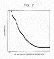
- Fig. 7 shows a result of simulation obtained by uniformly applying an external force of a certain magnitude to the entire membrane 310 in a projections-in-contact state shown in Fig.
- Fig. 8A to Fig. 8C include graphs expressing the relationship between the positional relationship between a rigid member and a projection and the magnitude of the deformation near the projection. As shown in Fig.
- Fig. 8C shows the relationship between the deviation quantity d between the rigid member and projection and a membrane contact voltage.
- the membrane contact voltage is high.
- the membrane contact voltage decreases. Accordingly, wherever the rigid member is disposed largely affects the deformation near the projection. When the rigid member is disposed so that the center of the rigid member coincides with the center of the projection, the deformation near the projection is minimized.
- the deposition is therefore effective.
- a structure shown in Fig. 9 that is a top view when parallelepiped rigid members 303 and cylindrical projections 304 are even partly layered when viewed from the upper surface, an effect of minimizing the deformations near the respective projections is exerted.
- the shape and disposition of the rigid members 303 viewed from the upper surface should be appropriately determined depending on a desired frequency characteristic.
- one parallelepiped rigid member 303 may be layered over at least parts of plural cylindrical projections 304 when viewed from the upper surface. Even in this structure, the plural projections 304 are disposed so that the upper electrode 305 is not layered over the plural projections 304.
- the rigid members 303 are disposed to be at least partly layered over the plural projections 304 when viewed from the upper surface.
- the structure would prove useful as a means for raising the membrane contact voltage in case the width of a hollow portion 302 is large and the rigidness in the width direction of the hollow portion is low.
- the number of projections 304 should be a minimum necessary value.
- the shape of the rigid members 303 may be cruciform. In this structure, at a position in a membrane between the projections 304 at which the rigid member 303 is located, the membrane gets thicker.
- the rigidness can be improved, and the contact voltage of the inter-projection membrane can be raised.
- the rigidness of the inter-projection membrane can be upgraded.
- the area of the rigid members 203 gets larger, the rigidness of the entire membrane gets higher, and a driving voltage gets higher.
- the cruciform rigid members 303 shown in Fig. 11 make it possible to raise the contact voltage of the inter-projection membrane without a large change in the driving voltage.
- the structures having rigid members disposed over the surface of the membrane have been described so far.
- the rigid members 303 may be embedded in the membrane 310.
- the shape of the membrane 310 is preferably flat, but may dilate or dent due to residual stresses of films included. As shown in Fig. 12 , by varying the positions at which the respective rigid members 303 are embedded, a residual stress distribution in the membrane 310 can be controlled. The dilated or dented shape of the membrane 310 can be controlled.
- the structure of a CMUT in accordance with an embodiment 2 will be described in conjunction with Fig. 13 .
- the CMUT includes a parallelepiped lower electrode 501 disposed over a substrate 506, a hollow portion 502 disposed over the lower electrode 501, and a parallelepiped upper electrode 505 disposed over the hollow portion 502.
- An insulating film 509 is formed to cover the lower electrode 501 between the lower electrode 501 and hollow portion 502, and an insulating film 508 is formed to cover the hollow portion 502 and lower electrode 501 between the upper electrode 505 and hollow portion 502.
- At least one or more cylindrical projections 504 jutting out from the top of the insulating film 509 to the hollow portion 502 are disposed in the hollow portion 502.
- the projections 504 are formed with the insulating film. Over the top of the insulating film 507, at least one or more parallelepiped rigid members 503 are disposed. Beam members that are the rigid members 503 may be, similarly to the insulating films 507, 508, and 509, made of a material such as a silicon oxide or silicon nitride, or may be made of another material. A membrane 510 including the insulating film 507, upper electrode 505, and insulating film 508 is vibrated in order to transmit an ultrasonic wave.
- the surfaces of the projections 504 opposed to the insulating film 508 with the hollow portion between them shall be called projection tops 514, and the surface of the insulating film 509 exposed to the hollow portion shall be called a hollow portion bottom 513.
- the surface of the membrane 510 exposed to the hollow portion shall be called a membrane undersurface 512.
- An incident that the projection tops 514 come into contact with the membrane undersurface 512 shall be called projection contact, and a voltage at that time shall be called a projection contact voltage.
- An incident that the membrane undersurface 512 comes into contact with the hollow portion bottom 513 shall be called membrane contact, and a voltage at that time shall be called a membrane contact voltage.
- a difference between the membrane contact voltage and projection contact voltage shall be called a margin voltage.
- the spacing between the rigid members 503 or projections 504 should be, similarly to the contents described in relation to the embodiment 1, determined based on the magnitude relationship between the membrane contact voltage and projection contact voltage. For example, when the membrane contact voltage is lower than the projection contact voltage, the spacing between the rigid members 503 or between the projections 504 is narrowed in order to raise the membrane contact voltage.
- a difference from the aforesaid embodiment 1 lies in a point that the projections 504 jut out from the hollow portion bottom 513 to the hollow portion 502.
- the structure becomes identical to the structure that is shown in Fig. 6 and that has the projections 304 jutted out from the membrane undersurface 312 to the hollow portion 302.
- the difference between a projection contact voltage and membrane contact voltage can be increased. Therefore, the same advantage as that of the ultrasonic transducer of the embodiment 1 can be provided.
- the disposition in which the centers of the rigid members 503 coincide with the centers of the projections 504 when viewed from the upper surface provides the greatest advantage. If the rigid members are even partly layered over the projections, an advantage is provided.
- the rigid members disposed over the surface of the membrane has been described so far.
- the rigid members 503 may be embedded in the membrane 510. This is advantageous as mentioned in relation to the embodiment 1 in that the shape of the membrane 510 can be readily controlled.
- CMUT cell includes a parallelepiped lower electrode 701, a hollow portion 702 disposed over the lower electrode 701, a parallelepiped upper electrode 705 disposed over the hollow portion 702, or the like.
- An insulating film 709 is formed to cover the lower electrode 701 between the lower electrode 701 and hollow portion 702, and an insulating film 708 is formed to cover the hollow portion 702 and lower electrode 701 between the upper electrode 705 and hollow portion 702.
- At least one or more cylindrical projections 704 that jut out from the undersurface of the insulating film 708 to the hollow portion 702 are disposed in the hollow portion 702.
- the projections 704 are formed with the insulating film.
- the projections 704 and insulating films 707, 708, and 709 are made of a silicon oxide, silicon nitride, or the like.
- Parallelepiped high-Young's modulus members 703 are embedded in a membrane 710. In Fig. 15 , the high-Young's modulus members 703 are embedded in the insulating film 707.
- the high-Young's modulus members 703 may be embedded in the insulating film 708, or may be embedded in both of the insulating film 707 and insulating film 708.
- the high-Young's modulus members 703 are made of a material whose Young's modulus is higher than that of the surrounding insulating film 707 or insulating film 708, for example, a metallic material such as tungsten or a ceramic material such as alumina, or formed by reforming the insulating film 707 or insulating film 708 through ion implantation so as to improve the Young's modulus.
- a metallic material such as tungsten or a ceramic material such as alumina
- the surfaces of the projections 704 opposed to the insulating film 709 with the hollow portion between them shall be called projection undersurfaces 711, and the surface of the insulating film 709 exposed to the hollow portion shall be called a hollow portion bottom 713.
- the surface of the membrane 710 exposed to the hollow portion shall be called a membrane undersurface 712.
- An incident that the projection undersurfaces 711 come into contact with the hollow portion bottom 713 shall be called projection contact, and a voltage at that time shall be called a projection contact voltage.
- An incident that the membrane undersurface 712 comes into contact with the hollow portion bottom 713 shall be called membrane contact, and a voltage at that time shall be called a membrane contact voltage.
- Fig. 15 is a cross-sectional diagram showing a section cut along a line A-A' in Fig. 16 .
- the projections 704 and others are seen through the high-Young's modulus members 703.
- the hollow portion 702 and upper electrode 705 they shall have a width in the lengthwise direction of a sheet of paper and a length in the sideways direction thereof.
- the high-Young's modulus members 703 they shall have a length in the lengthwise direction of the sheet of paper and a width in the sideways direction thereof.
- At least one or more projections 704 are disposed in the center in the width direction of the hollow portion 702 when viewed from the upper surface.
- the high-Young's modulus members 703 are disposed so that the centers thereof coincide with the centers of the projections 704 when viewed from the upper surface.
- At least one of the upper electrode 705 and lower electrode 701 is located at a position at which the electrode is not layered over the projections 704 when viewed from the upper surface.
- the upper electrode 705 is partly pierced and disposed so that the projections 704 and upper electrode 705 are not layered when viewed from the upper surface.
- the electrode to be pierced may be the lower electrode 701.
- the reason why the disposition is adopted is to increase an inter-electrode distance by piercing the electrode and thus decrease electric field strength for fear a strong electric field may be applied to each of the projections 704 and insulating film 709 and charge injection may thus take place in case a dc voltage or ac voltage is applied across the electrodes and the projection undersurfaces 711 come into contact with the hollow portion bottom 713 accordingly.
- the high-Young's modulus members 703 and projections 704 are equidistantly disposed in the length direction of the hollow portion. Alternatively, the high-Young's modulus members 703 and projections 704 may be non-equidistantly disposed.
- the high-Young's modulus members 703 and projections 704 are non-equidistantly disposed, plural membrane contact voltages are present in one CMUT. This is not preferred in terms of design. Therefore, the high-Young's modulus members 703 and projections 704 should be equidistantly disposed.
- the spacing between the high-Young's modulus members 703 or between the projections 704 may be determined based on the magnitude relationship between the membrane contact voltage and projection contact voltage. For example, if the membrane contact voltage is lower than the projection contact voltage, the spacing between the high-Young's modulus members 703 or between the projections 704 is narrowed in order to improve the membrane contact voltage.
- the feature of the embodiment 3 is, as shown in Fig. 15 and Fig. 16 , that in the CMUT having at least one of the upper electrode 705 and lower electrode 701 disposed at a position at which the electrode is not layered over the projections 704, which jut out to the hollow portion 702, when viewed from the upper surface, the high-Young's modulus members 703 included in the membrane 710 and the projections 704 are disposed to be even partly layered when viewed from the upper surface. Noted herein is a point that the high-Young's modulus members are disposed within the membrane in fields, in which the membrane is layered over the projections 704 when viewed from the upper surface, in order to locally upgrade rigidness.
- the difference between the projection contact voltage and membrane contact voltage can be made larger.
- membrane contact can be prevented.
- the membrane contact voltage may be partly lower than a design value because of a variance stemming from fabrication.
- the structure of a CMUT in accordance with an embodiment 4 will be described in conjunction with Fig. 17 .
- the CMUT includes a parallelepiped lower electrode 701 disposed over a substrate 706, a hollow portion 702 disposed over the lower electrode 701, and a parallelepiped upper electrode 705 disposed over the hollow portion 702.
- An insulating film 709 is formed to cover the lower electrode 701 between the lower electrode 701 and hollow portion 702, and an insulating film 708 is formed to cover the hollow portion 702 and lower electrode 701 between the upper electrode 705 and hollow portion 702.
- At least one or more cylindrical projections 704 jutting out from the top of the insulating film 709 to the hollow portion 702 are disposed in the hollow portion 702.
- the projections 704 are formed with the insulating film. Over the top of the insulating film 707, at least one or more parallelepiped high-Young's modulus members 703 are embedded.
- the surfaces of the projections 704 opposed to the insulating film 708 with the hollow portion between them shall be called projection tops 714, and the surface of the insulating film 709 exposed to the hollow portion shall be called a hollow portion bottom 713.
- the surface of a membrane 710 exposed to the hollow portion shall be called a membrane undersurface 712.
- An incident that the projection tops 714 come into contact with the membrane undersurface 712 shall be called a projection contact, and a voltage at that time shall be called a projection contact voltage.
- the spacing between the high-Young's modulus members 703 or projections 704 should be determined based on the magnitude relationship between the membrane contact voltage and projection contact voltage. For example, when the membrane contact voltage is lower than the projection contact voltage, the spacing between the high-Young's modulus members 703 or between the projections 704 is narrowed in order to raise the membrane contact voltage.
- a difference from the aforesaid embodiment 3 lies in a point that the projections 704 jut out from the hollow portion bottom 713 to the hollow portion 702.
- the membrane undersurface 712 comes into contact with the projection tops 714, the same state as the projections-in-contact state of the structure shown in Fig. 15 is attained. Therefore, even in the structure having the projections 704 jutted out from the hollow portion bottom 713, if the centers of the high-Young's modulus members coincide with the centers of the projections when viewed from the upper surface, the difference between the projection contact voltage and membrane contact voltage can be made larger, and the activity reliability of the CMUT can be improved.
- the same advantage as that of the ultrasonic transducer of the embodiment 3 can be provided.
- the ultrasonic transducer of the embodiment 3 if the high-Young's modulus members and projections are even partly layered when viewed from the upper surface, an advantage is provided.
- the structure is adopted, since the projections are absent from the membrane side of the CMUT vibration unit, the frequency characteristic of the CMUT can be readily designed.
- Fig. 18 is a top view showing an ultrasonic transducer of an embodiment 5.
- the ultrasonic transducer includes circular projections 804, a circular membrane 810, and circular rigid members 803 or high-Young's modulus members 805 disposed over the top of the membrane 810.
- the rigid members 803 and projections 804 are disposed in the center of the membrane 801 and at intermediate positions between the center of the membrane and each of the upper, lower, left, and right membrane edges.
- the rigid members 803 and projections 804 are disposed so that they are partly layered when viewed from the upper surface.
- the circular projections 804 are an example. A triangular, pentagonal, heptagonal, or any other polygonal shape will do.
- the circular shape is an example, but a triangular, pentagonal, heptagonal, or any other polygonal shape will do.
- the number of rigid members 803 or projections 804, and the disposition thereof may be determined based on the magnitude relationship between a projection contact voltage and a membrane contact voltage. For example, if the membrane contact voltage is lower than the projection contact voltage in the structure shown in Fig. 18 , the number of rigid members 803 or projections 804 should be increased. In that case, the dispositional positions should be points at which the membrane comes into contact with the projections with the membrane contact voltage.
- Fig. 19 is a top view showing an ultrasonic transducer of an embodiment 6.
- the ultrasonic transducer includes circular projections 904, an octagonal membrane 910, and circular rigid members 903 or high-Young's modulus members 905 disposed over the top of the membrane 910.
- the rigid members 903 and projections 904 are disposed in the center of the membrane 910 and around the center thereof.
- the rigid members 903 and projections 904 are disposed so that they are partly layered when viewed from the upper surface.
- the octagonal membrane 901 is an example. A triangular, pentagonal, heptagonal, or any other polygonal shape will do.
- the circular projections 904 are an example.
- a triangular, pentagonal, heptagonal, or any other polygonal shape will do. Even for the rigid members 903 or high-Young's modulus members 905, the circular shape is an example, but a triangular, pentagonal, heptagonal, or any other polygonal shape will do.
- the number of rigid members 903 or projections 904 and the disposition thereof may be determined based on the magnitude relationship between a projection contact voltage and membrane contact voltage. For example, if the membrane contact voltage is lower than the projection contact voltage in the structure shown in Fig. 19 , the number of rigid members 903 or projections 904 should be increased. In that case, the dispositional positions should be points at which the membrane comes into contact with the projections with the membrane contact voltage.
- An ultrasonic diagnostic equipment 1001 includes an ultrasonic probe 1002, a transmitting/receiving separation unit 1003, a transmission unit 1004, a bias unit 1006, a receiving unit 1008, a phasing and summation unit 1010, an image processing unit 1012, a display unit 1014, a control unit 1016, and an operation unit 1018.
- the ultrasonic probe 1002 is a device that is brought into contact with a subject and transmits or receives ultrasonic waves to or from the subject.
- the ultrasonic waves are transmitted from the ultrasonic probe 1002 to the subject, and reflected echo signals sent from the subject are received by the ultrasonic probe 1002.
- the ultrasonic transducer in accordance with any of the embodiments 1 to 6 is stored in the ultrasonic probe 1002, and electrically coupled to the transmitting/receiving separation unit 1003 to be described later.
- the transmission unit 1004 and bias unit 1006 are devices that feed a driving signal to the ultrasonic probe 1002.
- the receiving unit 1008 is a device that receives the reflected echo signals outputted from the ultrasonic probe 1002.
- the receiving unit 1008 further performs such processing as analog-to-digital conversion on the received reflected echo signals.
- the transmitting/receiving separation unit 1003 switches or separates transmitting and receiving, so that the driving signal can be passed from the transmission unit 1004 to the ultrasonic probe 1002 during transmission, or a receiving signal can be passed from the ultrasonic probe 1002 to the receiving unit 1008 during receiving.
- the phasing and summation unit 1010 is a device that phases and summates received reflected echo signals.
- the image processing unit 1010 is a device that constructs a diagnostic image (for example, a tomographic image or bloodstream image) on the basis of the phased and summated reflected echo signals.
- the display unit 1014 is a display device that displays the diagnostic image which has undergone image processing.
- the control unit 1016 is a device that controls the foregoing components.
- the operation unit 1018 is a device to be used to give instructions to the control unit 1016.
- the operation unit 1018 includes pieces of input equipment, for example, a trackball, a keyboard, and a mouse.
- the ultrasonic transducer of the present invention can be employed in an ultrasonic diagnostic equipment including an ultrasonic probe, a defect inspection apparatus for the interior of a structure, an object position sensing apparatus, a flow velocity measurement apparatus, or the like.
- a high transmission sound pressure and high receiving sensitivity can be realized.
- reliability in long-term driving can be improved.
Landscapes
- Health & Medical Sciences (AREA)
- Life Sciences & Earth Sciences (AREA)
- Engineering & Computer Science (AREA)
- Physics & Mathematics (AREA)
- General Health & Medical Sciences (AREA)
- Pathology (AREA)
- Surgery (AREA)
- Animal Behavior & Ethology (AREA)
- Veterinary Medicine (AREA)
- Public Health (AREA)
- Molecular Biology (AREA)
- Medical Informatics (AREA)
- Heart & Thoracic Surgery (AREA)
- Biomedical Technology (AREA)
- Biophysics (AREA)
- Nuclear Medicine, Radiotherapy & Molecular Imaging (AREA)
- Radiology & Medical Imaging (AREA)
- Gynecology & Obstetrics (AREA)
- Chemical & Material Sciences (AREA)
- Immunology (AREA)
- General Physics & Mathematics (AREA)
- Analytical Chemistry (AREA)
- Biochemistry (AREA)
- Mechanical Engineering (AREA)
- Power Engineering (AREA)
- Acoustics & Sound (AREA)
- Signal Processing (AREA)
- Transducers For Ultrasonic Waves (AREA)
- Ultra Sonic Daignosis Equipment (AREA)
- Investigating Or Analyzing Materials By The Use Of Ultrasonic Waves (AREA)
Claims (15)
- Ultraschallwandler, der eine untere Elektrode (201, 301, 501, 701, 801, 901), einen hohlen Abschnitt (202, 302, 502, 702), der über der unteren Elektrode (201, 301, 501, 701, 801, 901) gebildet ist und von einer Isolierschicht (207, 208, 209, 307, 308, 309, 507, 508, 509, 707, 708, 709) umschlossen ist, eine obere Elektrode (205, 305, 505, 705), die über dem hohlen Abschnitt (202, 302, 502, 702) gebildet ist, und mehrere Vorsprünge (204, 304, 504, 704, 804, 904) der Isolierschicht (207, 208, 209, 307, 308, 309, 507, 508, 509, 707, 708, 709), die in dem hohlen Abschnitt (202, 302, 502, 702) gebildet sind, umfasst, wobei:die untere Elektrode (201, 301, 501, 701, 801, 901) und/oder die obere Elektrode (205, 305, 505, 705) Abschnitte besitzen, die bei Betrachtung von einer oberen Oberfläche über einem Bereich liegen, in dem die Vorsprünge der Isolierschicht (204, 304, 504, 704, 804, 904) vorgesehen sind, und die durchlocht sind, so dass die Elektrode (201, 301, 501, 701, 801, 901, 205, 305, 505, 705) in einer vertikalen Richtung der Vorsprünge (204, 304, 504, 704, 804, 904) der Isolierschicht (207, 208, 209, 307, 308, 309, 507, 508, 509, 707, 708, 709) nicht vorhanden ist;dadurch gekennzeichnet, dass der Ultraschallwandler ferner mehrere starre Elemente (203, 303, 503, 803, 903) umfasst, die über dem hohlen Abschnitt (202, 302, 502, 702) gebildet sind, wobeidie starren Elemente (203, 303, 503, 803, 903) so angeordnet sind, dass die starren Elemente (203, 303, 503, 803, 903) Bereiche besitzen, die bei Betrachtung von der oberen Oberfläche über den jeweiligen Vorsprüngen (204, 304, 504, 704, 804, 904) der Isolierschicht (207, 208, 209, 307, 308, 309, 507, 508, 509, 707, 708, 709) liegen.
- Ultraschallwandler nach Anspruch 1, wobei:die starren Elemente (203, 303, 503, 803, 903) Trägerelemente sind; undeine Membran, die die Isolierschicht (207, 208, 209, 307, 308, 309, 507, 508, 509, 707, 708, 709), die obere Elektrode (205, 305, 505, 705) und die Trägerelemente enthält, einen Abschnitt besitzt, in dem die Trägerelemente vorhanden sind, und um die Dicke der Trägerelemente dicker ausgebildet ist als ein Abschnitt, in dem die Trägerelemente nicht vorhanden sind.
- Ultraschallwandler nach Anspruch 2, der ferner eine obere Isolierschicht (207, 307, 507, 707) umfasst, die so gebildet ist, dass sie die obere Elektrode (205, 305, 505, 705) und den hohlen Abschnitt (202, 302, 502, 702) abdeckt, wobei:
die Trägerelemente über der oberen Isolierschicht (207, 307, 507, 707) angeordnet sind. - Ultraschallwandler nach Anspruch 2, der ferner eine obere Isolierschicht (207, 307, 507, 707) umfasst, die so gebildet ist, dass sie die obere Elektrode (205, 305, 505, 705) und den hohlen Abschnitt (202, 302, 502, 702) abdeckt, wobei:
die Trägerelemente in die obere Isolierschicht (207, 307, 507, 707) eingebettet sind. - Ultraschallwandler nach Anspruch 2, wobei die starren Elemente (203, 303, 503, 803, 903) Elemente sind, die einen höheren Young-Modul besitzt als die Membran, die die Isolierschicht (207, 208, 209, 307, 308, 309, 507, 508, 509, 707, 708, 709), die obere Elektrode (205, 305, 505, 705) und die Trägerelemente enthält.
- Ultraschallwandler nach Anspruch 5, die ferner eine obere Isolierschicht (207, 307, 507, 707) umfasst, die so gebildet ist, dass sie die obere Elektrode und den hohlen Abschnitt abdeckt, wobei:
die Elemente mit hohem Young-Modul in die obere Isolierschicht (207, 307, 507, 707) eingebettet sind. - Ultraschallwandler nach Anspruch 6, wobei die Elemente mit hohem Young-Modul durch Einbetten eines Metallmaterials wie etwa Wolfram oder eines Keramikmaterials wie etwa Aluminiumoxid gebildet sind.
- Ultraschallwandler nach Anspruch 6, wobei die Elemente mit hohem Young-Modul durch Reformieren der oberen Isolierschicht (207, 307, 507, 707) durch Ionenimplantation gebildet sind.
- Ultraschallwandler nach Anspruch 1, wobei die starren Elemente (203, 303, 503, 803, 903) so angeordnet sind, dass die Zentren der starren Elemente (203, 303, 503, 803, 903) bei Betrachtung von der oberen Oberfläche mit den Zentren der Vorsprünge (204, 304, 504, 704, 804, 904) der Isolierschicht (207, 208, 209, 307, 308, 309, 507, 508, 509, 707, 708, 709) zusammenfallen.
- Ultraschallwandler nach Anspruch 1, wobei die starren Elemente (203, 303, 503, 803, 903) so angeordnet sind, dass ein starres Element (203, 303, 503, 803, 903) über mehreren Vorsprüngen (204, 304, 504, 704, 804, 904) der Isolierschicht liegt.
- Ultraschallwandler nach Anspruch 1, wobei die Vorsprünge (204, 304, 504, 704, 804, 904) der Isolierschicht (207, 208, 209, 307, 308, 309, 507, 508, 509, 707, 708, 709) über der Oberseite des hohlen Abschnitts (202, 302, 502, 702) angeordnet sind.
- Ultraschallwandler nach Anspruch 1, wobei die Vorsprünge (204, 304, 504, 704, 804, 904) der Isolierschicht (207, 208, 209, 307, 308, 309, 507, 508, 509, 707, 708, 709) über der Unterseite des hohlen Abschnitts (202, 302, 502, 702) angeordnet sind.
- Ultraschallwandler nach Anspruch 1, wobei die mehreren Vorsprünge (204, 304, 504, 704, 804, 904) der Isolierschicht (207, 208, 209, 307, 308, 309, 507, 508, 509, 707, 708, 709) und die mehreren starren Elemente (203, 303, 503, 803, 903) bei Betrachtung von der oberen Oberfläche gleichmäßig beabstandet angeordnet sind.
- Ultraschallwandler nach Anspruch 1, wobei der hohle Abschnitt (202, 302, 502, 702) bei Betrachtung von der oberen Oberfläche kreisförmig oder polygonförmig ist.
- Ultraschalldiagnoseanlage, die den Ultraschallwandler nach einem der Ansprüche 1 bis 14 und eine Vorbelastungseinheit umfasst.
Applications Claiming Priority (2)
| Application Number | Priority Date | Filing Date | Title |
|---|---|---|---|
| JP2010232618 | 2010-10-15 | ||
| PCT/JP2011/073582 WO2012050172A1 (ja) | 2010-10-15 | 2011-10-13 | 超音波トランスデューサおよびそれを用いた超音波診断装置 |
Publications (3)
| Publication Number | Publication Date |
|---|---|
| EP2629549A1 EP2629549A1 (de) | 2013-08-21 |
| EP2629549A4 EP2629549A4 (de) | 2017-05-17 |
| EP2629549B1 true EP2629549B1 (de) | 2019-01-23 |
Family
ID=45938393
Family Applications (1)
| Application Number | Title | Priority Date | Filing Date |
|---|---|---|---|
| EP11832603.2A Active EP2629549B1 (de) | 2010-10-15 | 2011-10-13 | Ultraschallwandler und ultraschalldiagnosevorrichtung damit |
Country Status (6)
| Country | Link |
|---|---|
| US (1) | US9941817B2 (de) |
| EP (1) | EP2629549B1 (de) |
| JP (1) | JP5486689B2 (de) |
| KR (1) | KR101492033B1 (de) |
| CN (1) | CN103155597B (de) |
| WO (1) | WO2012050172A1 (de) |
Families Citing this family (22)
| Publication number | Priority date | Publication date | Assignee | Title |
|---|---|---|---|---|
| CN102440005B (zh) * | 2009-05-25 | 2014-09-24 | 株式会社日立医疗器械 | 超声波换能器及利用该超声波换能器的超声波诊断装置 |
| JP6065421B2 (ja) * | 2012-06-15 | 2017-01-25 | セイコーエプソン株式会社 | 超音波プローブおよび超音波検査装置 |
| JP2015023994A (ja) * | 2013-07-26 | 2015-02-05 | セイコーエプソン株式会社 | 超音波測定装置、超音波ヘッドユニット、超音波プローブ及び超音波画像装置 |
| CN106661535B (zh) * | 2014-01-21 | 2021-03-02 | 普罗美迪卡生物电子学公司 | 用于超声波测试的设备 |
| KR20160021559A (ko) * | 2014-08-18 | 2016-02-26 | 삼성전자주식회사 | 나노필라 구조를 가진 정전용량 미세가공 초음파 변환기 및 그 제조방법 |
| JP2016101417A (ja) * | 2014-11-28 | 2016-06-02 | キヤノン株式会社 | 静電容量型音響波トランスデューサ及びこれを備えた被検体情報取得装置 |
| JP6613628B2 (ja) * | 2015-05-28 | 2019-12-04 | セイコーエプソン株式会社 | 圧電デバイスおよびプローブ並びに電子機器および超音波画像装置 |
| JP6470406B2 (ja) * | 2015-05-29 | 2019-02-13 | 株式会社日立製作所 | 超音波トランスデューサおよび超音波検査装置 |
| CN108352439B (zh) * | 2015-10-27 | 2021-11-26 | 株式会社村田制作所 | 压电器件以及压电器件的制造方法 |
| JP6471242B2 (ja) * | 2015-11-13 | 2019-02-13 | 株式会社日立製作所 | Mems素子およびその製造方法 |
| US10006888B2 (en) * | 2016-04-21 | 2018-06-26 | The Boeing Company | MEMS transducers in a phased array coupled to a flexible substrate using carbon nanotubes for conformal ultrasound scanning |
| JP6763731B2 (ja) * | 2016-09-28 | 2020-09-30 | 株式会社日立製作所 | 超音波トランスデューサ、その製造方法および超音波撮像装置 |
| US9813831B1 (en) | 2016-11-29 | 2017-11-07 | Cirrus Logic, Inc. | Microelectromechanical systems microphone with electrostatic force feedback to measure sound pressure |
| US9900707B1 (en) * | 2016-11-29 | 2018-02-20 | Cirrus Logic, Inc. | Biasing of electromechanical systems microphone with alternating-current voltage waveform |
| WO2018236786A1 (en) * | 2017-06-20 | 2018-12-27 | Butterfly Network, Inc. | Analog to digital signal conversion in ultrasound device |
| JP6948216B2 (ja) * | 2017-10-13 | 2021-10-13 | 株式会社日立製作所 | 超音波送受信装置および超音波トランスデュ−サ |
| CN107957273B (zh) * | 2018-01-16 | 2024-05-03 | 北京先通康桥医药科技有限公司 | 具有触压和超声功能的传感器 |
| JP7410935B2 (ja) | 2018-05-24 | 2024-01-10 | ザ リサーチ ファウンデーション フォー ザ ステイト ユニバーシティー オブ ニューヨーク | 容量性センサ |
| JP2019212992A (ja) | 2018-05-31 | 2019-12-12 | キヤノン株式会社 | 静電容量型トランスデューサ、及びその製造方法 |
| KR102253210B1 (ko) * | 2020-08-06 | 2021-05-18 | 한국과학기술원 | 전하 포획층을 가지는 정전용량형 미세가공 초음파 트랜스듀서 및 이의 제조 방법 |
| TWI800437B (zh) * | 2022-08-02 | 2023-04-21 | 友達光電股份有限公司 | 超音波換能裝置 |
| TWI892270B (zh) * | 2023-10-24 | 2025-08-01 | 佳世達科技股份有限公司 | 超音波換能裝置及應用其之超音波探頭 |
Family Cites Families (19)
| Publication number | Priority date | Publication date | Assignee | Title |
|---|---|---|---|---|
| US5774423A (en) * | 1995-12-15 | 1998-06-30 | Innovative Transducers Inc. | Acoustic sensor and array thereof |
| JPH11169365A (ja) * | 1997-11-28 | 1999-06-29 | Hitachi Medical Corp | 超音波診断装置 |
| US6467879B1 (en) * | 2000-10-16 | 2002-10-22 | Xerox Corporation | Method and apparatus for preventing degradation of electrostatically actuated devices |
| CA2406684A1 (en) * | 2001-10-05 | 2003-04-05 | Queen's University At Kingston | Ultrasound transducer array |
| US6958255B2 (en) | 2002-08-08 | 2005-10-25 | The Board Of Trustees Of The Leland Stanford Junior University | Micromachined ultrasonic transducers and method of fabrication |
| US7530952B2 (en) | 2004-04-01 | 2009-05-12 | The Board Of Trustees Of The Leland Stanford Junior University | Capacitive ultrasonic transducers with isolation posts |
| US20060004289A1 (en) | 2004-06-30 | 2006-01-05 | Wei-Cheng Tian | High sensitivity capacitive micromachined ultrasound transducer |
| JP4735117B2 (ja) | 2005-08-08 | 2011-07-27 | 栗田工業株式会社 | 製紙方法 |
| JP4724501B2 (ja) * | 2005-09-06 | 2011-07-13 | 株式会社日立製作所 | 超音波トランスデューサおよびその製造方法 |
| CN104646260B (zh) * | 2005-10-18 | 2018-08-28 | 株式会社日立制作所 | 超声波探头 |
| JP4909279B2 (ja) * | 2005-10-18 | 2012-04-04 | 株式会社日立製作所 | 超音波探触子 |
| JP2008099036A (ja) | 2006-10-12 | 2008-04-24 | Olympus Medical Systems Corp | 超音波トランスデューサ、超音波探触子及び超音波診断装置 |
| JP5408937B2 (ja) | 2007-09-25 | 2014-02-05 | キヤノン株式会社 | 電気機械変換素子及びその製造方法 |
| WO2009041675A1 (en) * | 2007-09-25 | 2009-04-02 | Canon Kabushiki Kaisha | Electrostatic transducer and manufacturing method therefor |
| US8559274B2 (en) * | 2007-12-03 | 2013-10-15 | Kolo Technologies, Inc. | Dual-mode operation micromachined ultrasonic transducer |
| US8235906B2 (en) * | 2007-12-31 | 2012-08-07 | The Brigham And Women's Hospital, Inc. | System and method for accelerated focused ultrasound imaging |
| US8467559B2 (en) * | 2008-02-20 | 2013-06-18 | Shandong Gettop Acoustic Co., Ltd. | Silicon microphone without dedicated backplate |
| JP2010004199A (ja) | 2008-06-19 | 2010-01-07 | Hitachi Ltd | 超音波トランスデューサおよびその製造方法 |
| WO2010053032A1 (ja) * | 2008-11-04 | 2010-05-14 | オリンパスメディカルシステムズ株式会社 | 音響振動子及び画像生成装置 |
-
2011
- 2011-10-13 EP EP11832603.2A patent/EP2629549B1/de active Active
- 2011-10-13 KR KR1020137009318A patent/KR101492033B1/ko not_active Expired - Fee Related
- 2011-10-13 WO PCT/JP2011/073582 patent/WO2012050172A1/ja not_active Ceased
- 2011-10-13 JP JP2012538715A patent/JP5486689B2/ja active Active
- 2011-10-13 CN CN201180048454.0A patent/CN103155597B/zh active Active
- 2011-10-13 US US13/879,439 patent/US9941817B2/en active Active
Non-Patent Citations (1)
| Title |
|---|
| None * |
Also Published As
| Publication number | Publication date |
|---|---|
| EP2629549A1 (de) | 2013-08-21 |
| KR101492033B1 (ko) | 2015-02-10 |
| WO2012050172A1 (ja) | 2012-04-19 |
| CN103155597B (zh) | 2016-06-08 |
| US9941817B2 (en) | 2018-04-10 |
| JPWO2012050172A1 (ja) | 2014-02-24 |
| JP5486689B2 (ja) | 2014-05-07 |
| CN103155597A (zh) | 2013-06-12 |
| US20130241345A1 (en) | 2013-09-19 |
| EP2629549A4 (de) | 2017-05-17 |
| KR20130080040A (ko) | 2013-07-11 |
Similar Documents
| Publication | Publication Date | Title |
|---|---|---|
| EP2629549B1 (de) | Ultraschallwandler und ultraschalldiagnosevorrichtung damit | |
| US9925561B2 (en) | Capacitive micromachined ultrasonic transducer with multiple deflectable membranes | |
| US8617078B2 (en) | Ultrasonic transducer and ultrasonic diagnostic device using same | |
| EP3037178B1 (de) | Kapazitiver mikrobearbeiteter ultraschallwandler und testobjekterfassungsvorrichtung mit kapazitivem mikrobearbeitetem ultraschallwandler | |
| CN102440005B (zh) | 超声波换能器及利用该超声波换能器的超声波诊断装置 | |
| JP4730162B2 (ja) | 超音波送受信デバイス,超音波探触子およびその製造方法 | |
| US8869622B2 (en) | Capacitive electromechanical transducer apparatus and method for adjusting its sensitivity | |
| EP3559972B1 (de) | Systeme und verfahren zum betrieb von kapazitiven mikroelektromechanischen funkfrequenzschaltern | |
| EP2152024A1 (de) | Ultraschallwandler und ultraschall-bildgebervorrichtung | |
| KR20110119828A (ko) | 기계적 붕괴 보유를 갖는 사전 붕괴된 cmut | |
| CN102639258A (zh) | 用于电容式机电变换器的控制设备以及控制电容式机电变换器的方法 | |
| JP4958631B2 (ja) | 超音波送受信デバイス及びそれを用いた超音波探触子 | |
| CN108886660B (zh) | 超声波换能器、超声波换能器的制造方法以及超声波拍摄装置 | |
| JP2009071395A (ja) | 超音波受信素子及びこれを用いた超音波トランスデューサ | |
| JP2019075831A (ja) | 静電容量型音響波トランスデューサ及びこれを備えた被検体情報取得装置 |
Legal Events
| Date | Code | Title | Description |
|---|---|---|---|
| PUAI | Public reference made under article 153(3) epc to a published international application that has entered the european phase |
Free format text: ORIGINAL CODE: 0009012 |
|
| 17P | Request for examination filed |
Effective date: 20130515 |
|
| AK | Designated contracting states |
Kind code of ref document: A1 Designated state(s): AL AT BE BG CH CY CZ DE DK EE ES FI FR GB GR HR HU IE IS IT LI LT LU LV MC MK MT NL NO PL PT RO RS SE SI SK SM TR |
|
| DAX | Request for extension of the european patent (deleted) | ||
| RAP1 | Party data changed (applicant data changed or rights of an application transferred) |
Owner name: HITACHI, LTD. |
|
| RA4 | Supplementary search report drawn up and despatched (corrected) |
Effective date: 20170418 |
|
| RIC1 | Information provided on ipc code assigned before grant |
Ipc: G01N 29/24 20060101ALI20170410BHEP Ipc: H04R 19/04 20060101ALN20170410BHEP Ipc: A61B 8/00 20060101ALI20170410BHEP Ipc: B06B 1/02 20060101AFI20170410BHEP |
|
| STAA | Information on the status of an ep patent application or granted ep patent |
Free format text: STATUS: EXAMINATION IS IN PROGRESS |
|
| RIC1 | Information provided on ipc code assigned before grant |
Ipc: B06B 1/02 20060101AFI20180305BHEP Ipc: H04R 19/04 20060101ALN20180305BHEP Ipc: G01N 29/24 20060101ALI20180305BHEP Ipc: A61B 8/00 20060101ALI20180305BHEP |
|
| 17Q | First examination report despatched |
Effective date: 20180322 |
|
| REG | Reference to a national code |
Ref country code: DE Ref legal event code: R079 Ref document number: 602011055981 Country of ref document: DE Free format text: PREVIOUS MAIN CLASS: H04R0019000000 Ipc: B06B0001020000 |
|
| GRAP | Despatch of communication of intention to grant a patent |
Free format text: ORIGINAL CODE: EPIDOSNIGR1 |
|
| STAA | Information on the status of an ep patent application or granted ep patent |
Free format text: STATUS: GRANT OF PATENT IS INTENDED |
|
| RIC1 | Information provided on ipc code assigned before grant |
Ipc: H04R 19/04 20060101ALN20180720BHEP Ipc: A61B 8/00 20060101ALI20180720BHEP Ipc: B06B 1/02 20060101AFI20180720BHEP Ipc: G01N 29/24 20060101ALI20180720BHEP |
|
| INTG | Intention to grant announced |
Effective date: 20180806 |
|
| GRAS | Grant fee paid |
Free format text: ORIGINAL CODE: EPIDOSNIGR3 |
|
| GRAA | (expected) grant |
Free format text: ORIGINAL CODE: 0009210 |
|
| STAA | Information on the status of an ep patent application or granted ep patent |
Free format text: STATUS: THE PATENT HAS BEEN GRANTED |
|
| AK | Designated contracting states |
Kind code of ref document: B1 Designated state(s): AL AT BE BG CH CY CZ DE DK EE ES FI FR GB GR HR HU IE IS IT LI LT LU LV MC MK MT NL NO PL PT RO RS SE SI SK SM TR |
|
| REG | Reference to a national code |
Ref country code: GB Ref legal event code: FG4D |
|
| RIN1 | Information on inventor provided before grant (corrected) |
Inventor name: TAKEZAKI TAIICHI Inventor name: MACHIDA SHUNTARO |
|
| REG | Reference to a national code |
Ref country code: CH Ref legal event code: EP |
|
| REG | Reference to a national code |
Ref country code: AT Ref legal event code: REF Ref document number: 1091032 Country of ref document: AT Kind code of ref document: T Effective date: 20190215 |
|
| REG | Reference to a national code |
Ref country code: IE Ref legal event code: FG4D |
|
| REG | Reference to a national code |
Ref country code: DE Ref legal event code: R096 Ref document number: 602011055981 Country of ref document: DE |
|
| REG | Reference to a national code |
Ref country code: NL Ref legal event code: MP Effective date: 20190123 |
|
| PG25 | Lapsed in a contracting state [announced via postgrant information from national office to epo] |
Ref country code: NL Free format text: LAPSE BECAUSE OF FAILURE TO SUBMIT A TRANSLATION OF THE DESCRIPTION OR TO PAY THE FEE WITHIN THE PRESCRIBED TIME-LIMIT Effective date: 20190123 |
|
| PG25 | Lapsed in a contracting state [announced via postgrant information from national office to epo] |
Ref country code: PL Free format text: LAPSE BECAUSE OF FAILURE TO SUBMIT A TRANSLATION OF THE DESCRIPTION OR TO PAY THE FEE WITHIN THE PRESCRIBED TIME-LIMIT Effective date: 20190123 Ref country code: PT Free format text: LAPSE BECAUSE OF FAILURE TO SUBMIT A TRANSLATION OF THE DESCRIPTION OR TO PAY THE FEE WITHIN THE PRESCRIBED TIME-LIMIT Effective date: 20190523 Ref country code: FI Free format text: LAPSE BECAUSE OF FAILURE TO SUBMIT A TRANSLATION OF THE DESCRIPTION OR TO PAY THE FEE WITHIN THE PRESCRIBED TIME-LIMIT Effective date: 20190123 Ref country code: NO Free format text: LAPSE BECAUSE OF FAILURE TO SUBMIT A TRANSLATION OF THE DESCRIPTION OR TO PAY THE FEE WITHIN THE PRESCRIBED TIME-LIMIT Effective date: 20190423 Ref country code: SE Free format text: LAPSE BECAUSE OF FAILURE TO SUBMIT A TRANSLATION OF THE DESCRIPTION OR TO PAY THE FEE WITHIN THE PRESCRIBED TIME-LIMIT Effective date: 20190123 Ref country code: ES Free format text: LAPSE BECAUSE OF FAILURE TO SUBMIT A TRANSLATION OF THE DESCRIPTION OR TO PAY THE FEE WITHIN THE PRESCRIBED TIME-LIMIT Effective date: 20190123 Ref country code: LT Free format text: LAPSE BECAUSE OF FAILURE TO SUBMIT A TRANSLATION OF THE DESCRIPTION OR TO PAY THE FEE WITHIN THE PRESCRIBED TIME-LIMIT Effective date: 20190123 |
|
| REG | Reference to a national code |
Ref country code: AT Ref legal event code: MK05 Ref document number: 1091032 Country of ref document: AT Kind code of ref document: T Effective date: 20190123 |
|
| PG25 | Lapsed in a contracting state [announced via postgrant information from national office to epo] |
Ref country code: HR Free format text: LAPSE BECAUSE OF FAILURE TO SUBMIT A TRANSLATION OF THE DESCRIPTION OR TO PAY THE FEE WITHIN THE PRESCRIBED TIME-LIMIT Effective date: 20190123 Ref country code: GR Free format text: LAPSE BECAUSE OF FAILURE TO SUBMIT A TRANSLATION OF THE DESCRIPTION OR TO PAY THE FEE WITHIN THE PRESCRIBED TIME-LIMIT Effective date: 20190424 Ref country code: BG Free format text: LAPSE BECAUSE OF FAILURE TO SUBMIT A TRANSLATION OF THE DESCRIPTION OR TO PAY THE FEE WITHIN THE PRESCRIBED TIME-LIMIT Effective date: 20190423 Ref country code: LV Free format text: LAPSE BECAUSE OF FAILURE TO SUBMIT A TRANSLATION OF THE DESCRIPTION OR TO PAY THE FEE WITHIN THE PRESCRIBED TIME-LIMIT Effective date: 20190123 Ref country code: IS Free format text: LAPSE BECAUSE OF FAILURE TO SUBMIT A TRANSLATION OF THE DESCRIPTION OR TO PAY THE FEE WITHIN THE PRESCRIBED TIME-LIMIT Effective date: 20190523 Ref country code: RS Free format text: LAPSE BECAUSE OF FAILURE TO SUBMIT A TRANSLATION OF THE DESCRIPTION OR TO PAY THE FEE WITHIN THE PRESCRIBED TIME-LIMIT Effective date: 20190123 |
|
| REG | Reference to a national code |
Ref country code: DE Ref legal event code: R097 Ref document number: 602011055981 Country of ref document: DE |
|
| PG25 | Lapsed in a contracting state [announced via postgrant information from national office to epo] |
Ref country code: AL Free format text: LAPSE BECAUSE OF FAILURE TO SUBMIT A TRANSLATION OF THE DESCRIPTION OR TO PAY THE FEE WITHIN THE PRESCRIBED TIME-LIMIT Effective date: 20190123 Ref country code: CZ Free format text: LAPSE BECAUSE OF FAILURE TO SUBMIT A TRANSLATION OF THE DESCRIPTION OR TO PAY THE FEE WITHIN THE PRESCRIBED TIME-LIMIT Effective date: 20190123 Ref country code: RO Free format text: LAPSE BECAUSE OF FAILURE TO SUBMIT A TRANSLATION OF THE DESCRIPTION OR TO PAY THE FEE WITHIN THE PRESCRIBED TIME-LIMIT Effective date: 20190123 Ref country code: IT Free format text: LAPSE BECAUSE OF FAILURE TO SUBMIT A TRANSLATION OF THE DESCRIPTION OR TO PAY THE FEE WITHIN THE PRESCRIBED TIME-LIMIT Effective date: 20190123 Ref country code: DK Free format text: LAPSE BECAUSE OF FAILURE TO SUBMIT A TRANSLATION OF THE DESCRIPTION OR TO PAY THE FEE WITHIN THE PRESCRIBED TIME-LIMIT Effective date: 20190123 Ref country code: EE Free format text: LAPSE BECAUSE OF FAILURE TO SUBMIT A TRANSLATION OF THE DESCRIPTION OR TO PAY THE FEE WITHIN THE PRESCRIBED TIME-LIMIT Effective date: 20190123 Ref country code: SK Free format text: LAPSE BECAUSE OF FAILURE TO SUBMIT A TRANSLATION OF THE DESCRIPTION OR TO PAY THE FEE WITHIN THE PRESCRIBED TIME-LIMIT Effective date: 20190123 |
|
| PG25 | Lapsed in a contracting state [announced via postgrant information from national office to epo] |
Ref country code: SM Free format text: LAPSE BECAUSE OF FAILURE TO SUBMIT A TRANSLATION OF THE DESCRIPTION OR TO PAY THE FEE WITHIN THE PRESCRIBED TIME-LIMIT Effective date: 20190123 |
|
| PLBE | No opposition filed within time limit |
Free format text: ORIGINAL CODE: 0009261 |
|
| STAA | Information on the status of an ep patent application or granted ep patent |
Free format text: STATUS: NO OPPOSITION FILED WITHIN TIME LIMIT |
|
| PG25 | Lapsed in a contracting state [announced via postgrant information from national office to epo] |
Ref country code: AT Free format text: LAPSE BECAUSE OF FAILURE TO SUBMIT A TRANSLATION OF THE DESCRIPTION OR TO PAY THE FEE WITHIN THE PRESCRIBED TIME-LIMIT Effective date: 20190123 |
|
| 26N | No opposition filed |
Effective date: 20191024 |
|
| PG25 | Lapsed in a contracting state [announced via postgrant information from national office to epo] |
Ref country code: SI Free format text: LAPSE BECAUSE OF FAILURE TO SUBMIT A TRANSLATION OF THE DESCRIPTION OR TO PAY THE FEE WITHIN THE PRESCRIBED TIME-LIMIT Effective date: 20190123 |
|
| PG25 | Lapsed in a contracting state [announced via postgrant information from national office to epo] |
Ref country code: TR Free format text: LAPSE BECAUSE OF FAILURE TO SUBMIT A TRANSLATION OF THE DESCRIPTION OR TO PAY THE FEE WITHIN THE PRESCRIBED TIME-LIMIT Effective date: 20190123 |
|
| PG25 | Lapsed in a contracting state [announced via postgrant information from national office to epo] |
Ref country code: MC Free format text: LAPSE BECAUSE OF FAILURE TO SUBMIT A TRANSLATION OF THE DESCRIPTION OR TO PAY THE FEE WITHIN THE PRESCRIBED TIME-LIMIT Effective date: 20190123 |
|
| REG | Reference to a national code |
Ref country code: CH Ref legal event code: PL |
|
| PG25 | Lapsed in a contracting state [announced via postgrant information from national office to epo] |
Ref country code: LI Free format text: LAPSE BECAUSE OF NON-PAYMENT OF DUE FEES Effective date: 20191031 Ref country code: CH Free format text: LAPSE BECAUSE OF NON-PAYMENT OF DUE FEES Effective date: 20191031 Ref country code: LU Free format text: LAPSE BECAUSE OF NON-PAYMENT OF DUE FEES Effective date: 20191013 |
|
| REG | Reference to a national code |
Ref country code: BE Ref legal event code: MM Effective date: 20191031 |
|
| PG25 | Lapsed in a contracting state [announced via postgrant information from national office to epo] |
Ref country code: BE Free format text: LAPSE BECAUSE OF NON-PAYMENT OF DUE FEES Effective date: 20191031 |
|
| GBPC | Gb: european patent ceased through non-payment of renewal fee |
Effective date: 20191013 |
|
| PG25 | Lapsed in a contracting state [announced via postgrant information from national office to epo] |
Ref country code: FR Free format text: LAPSE BECAUSE OF NON-PAYMENT OF DUE FEES Effective date: 20191031 Ref country code: GB Free format text: LAPSE BECAUSE OF NON-PAYMENT OF DUE FEES Effective date: 20191013 Ref country code: IE Free format text: LAPSE BECAUSE OF NON-PAYMENT OF DUE FEES Effective date: 20191013 |
|
| PG25 | Lapsed in a contracting state [announced via postgrant information from national office to epo] |
Ref country code: CY Free format text: LAPSE BECAUSE OF FAILURE TO SUBMIT A TRANSLATION OF THE DESCRIPTION OR TO PAY THE FEE WITHIN THE PRESCRIBED TIME-LIMIT Effective date: 20190123 |
|
| PG25 | Lapsed in a contracting state [announced via postgrant information from national office to epo] |
Ref country code: HU Free format text: LAPSE BECAUSE OF FAILURE TO SUBMIT A TRANSLATION OF THE DESCRIPTION OR TO PAY THE FEE WITHIN THE PRESCRIBED TIME-LIMIT; INVALID AB INITIO Effective date: 20111013 Ref country code: MT Free format text: LAPSE BECAUSE OF FAILURE TO SUBMIT A TRANSLATION OF THE DESCRIPTION OR TO PAY THE FEE WITHIN THE PRESCRIBED TIME-LIMIT Effective date: 20190123 |
|
| REG | Reference to a national code |
Ref country code: DE Ref legal event code: R081 Ref document number: 602011055981 Country of ref document: DE Owner name: FUJIFILM HEALTHCARE CORPORATION, KASHIWA-SHI, JP Free format text: FORMER OWNER: HITACHI, LTD., TOKYO, JP Ref country code: DE Ref legal event code: R081 Ref document number: 602011055981 Country of ref document: DE Owner name: FUJIFILM CORPORATION, JP Free format text: FORMER OWNER: HITACHI, LTD., TOKYO, JP |
|
| PG25 | Lapsed in a contracting state [announced via postgrant information from national office to epo] |
Ref country code: MK Free format text: LAPSE BECAUSE OF FAILURE TO SUBMIT A TRANSLATION OF THE DESCRIPTION OR TO PAY THE FEE WITHIN THE PRESCRIBED TIME-LIMIT Effective date: 20190123 |
|
| P01 | Opt-out of the competence of the unified patent court (upc) registered |
Effective date: 20230522 |
|
| REG | Reference to a national code |
Ref country code: DE Ref legal event code: R081 Ref document number: 602011055981 Country of ref document: DE Owner name: FUJIFILM CORPORATION, JP Free format text: FORMER OWNER: FUJIFILM HEALTHCARE CORPORATION, KASHIWA-SHI, CHIBA, JP |
|
| PGFP | Annual fee paid to national office [announced via postgrant information from national office to epo] |
Ref country code: DE Payment date: 20250902 Year of fee payment: 15 |