EP2631999A1 - Appareil laser et appareil de traitement laser équipé de celui-ci - Google Patents
Appareil laser et appareil de traitement laser équipé de celui-ci Download PDFInfo
- Publication number
- EP2631999A1 EP2631999A1 EP10858601.7A EP10858601A EP2631999A1 EP 2631999 A1 EP2631999 A1 EP 2631999A1 EP 10858601 A EP10858601 A EP 10858601A EP 2631999 A1 EP2631999 A1 EP 2631999A1
- Authority
- EP
- European Patent Office
- Prior art keywords
- laser
- laser beam
- fiber
- workpiece
- core
- Prior art date
- Legal status (The legal status is an assumption and is not a legal conclusion. Google has not performed a legal analysis and makes no representation as to the accuracy of the status listed.)
- Granted
Links
Images







Classifications
-
- H—ELECTRICITY
- H01—ELECTRIC ELEMENTS
- H01S—DEVICES USING THE PROCESS OF LIGHT AMPLIFICATION BY STIMULATED EMISSION OF RADIATION [LASER] TO AMPLIFY OR GENERATE LIGHT; DEVICES USING STIMULATED EMISSION OF ELECTROMAGNETIC RADIATION IN WAVE RANGES OTHER THAN OPTICAL
- H01S3/00—Lasers, i.e. devices using stimulated emission of electromagnetic radiation in the infrared, visible or ultraviolet wave range
- H01S3/05—Construction or shape of optical resonators; Accommodation of active medium therein; Shape of active medium
- H01S3/06—Construction or shape of active medium
- H01S3/063—Waveguide lasers, i.e. whereby the dimensions of the waveguide are of the order of the light wavelength
- H01S3/067—Fibre lasers
- H01S3/06708—Constructional details of the fibre, e.g. compositions, cross-section, shape or tapering
- H01S3/06716—Fibre compositions or doping with active elements
-
- B—PERFORMING OPERATIONS; TRANSPORTING
- B23—MACHINE TOOLS; METAL-WORKING NOT OTHERWISE PROVIDED FOR
- B23K—SOLDERING OR UNSOLDERING; WELDING; CLADDING OR PLATING BY SOLDERING OR WELDING; CUTTING BY APPLYING HEAT LOCALLY, e.g. FLAME CUTTING; WORKING BY LASER BEAM
- B23K26/00—Working by laser beam, e.g. welding, cutting or boring
- B23K26/02—Positioning or observing the workpiece, e.g. with respect to the point of impact; Aligning, aiming or focusing the laser beam
- B23K26/06—Shaping the laser beam, e.g. by masks or multi-focusing
- B23K26/0604—Shaping the laser beam, e.g. by masks or multi-focusing by a combination of beams
- B23K26/0613—Shaping the laser beam, e.g. by masks or multi-focusing by a combination of beams having a common axis
-
- H—ELECTRICITY
- H01—ELECTRIC ELEMENTS
- H01S—DEVICES USING THE PROCESS OF LIGHT AMPLIFICATION BY STIMULATED EMISSION OF RADIATION [LASER] TO AMPLIFY OR GENERATE LIGHT; DEVICES USING STIMULATED EMISSION OF ELECTROMAGNETIC RADIATION IN WAVE RANGES OTHER THAN OPTICAL
- H01S3/00—Lasers, i.e. devices using stimulated emission of electromagnetic radiation in the infrared, visible or ultraviolet wave range
- H01S3/005—Optical devices external to the laser cavity, specially adapted for lasers, e.g. for homogenisation of the beam or for manipulating laser pulses, e.g. pulse shaping
-
- H—ELECTRICITY
- H01—ELECTRIC ELEMENTS
- H01S—DEVICES USING THE PROCESS OF LIGHT AMPLIFICATION BY STIMULATED EMISSION OF RADIATION [LASER] TO AMPLIFY OR GENERATE LIGHT; DEVICES USING STIMULATED EMISSION OF ELECTROMAGNETIC RADIATION IN WAVE RANGES OTHER THAN OPTICAL
- H01S3/00—Lasers, i.e. devices using stimulated emission of electromagnetic radiation in the infrared, visible or ultraviolet wave range
- H01S3/05—Construction or shape of optical resonators; Accommodation of active medium therein; Shape of active medium
- H01S3/06—Construction or shape of active medium
- H01S3/063—Waveguide lasers, i.e. whereby the dimensions of the waveguide are of the order of the light wavelength
- H01S3/067—Fibre lasers
- H01S3/0675—Resonators including a grating structure, e.g. distributed Bragg reflectors [DBR] or distributed feedback [DFB] fibre lasers
-
- H—ELECTRICITY
- H01—ELECTRIC ELEMENTS
- H01S—DEVICES USING THE PROCESS OF LIGHT AMPLIFICATION BY STIMULATED EMISSION OF RADIATION [LASER] TO AMPLIFY OR GENERATE LIGHT; DEVICES USING STIMULATED EMISSION OF ELECTROMAGNETIC RADIATION IN WAVE RANGES OTHER THAN OPTICAL
- H01S3/00—Lasers, i.e. devices using stimulated emission of electromagnetic radiation in the infrared, visible or ultraviolet wave range
- H01S3/09—Processes or apparatus for excitation, e.g. pumping
- H01S3/091—Processes or apparatus for excitation, e.g. pumping using optical pumping
- H01S3/094—Processes or apparatus for excitation, e.g. pumping using optical pumping by coherent light
- H01S3/094003—Processes or apparatus for excitation, e.g. pumping using optical pumping by coherent light the pumped medium being a fibre
- H01S3/094011—Processes or apparatus for excitation, e.g. pumping using optical pumping by coherent light the pumped medium being a fibre with bidirectional pumping, i.e. with injection of the pump light from both two ends of the fibre
-
- H—ELECTRICITY
- H01—ELECTRIC ELEMENTS
- H01S—DEVICES USING THE PROCESS OF LIGHT AMPLIFICATION BY STIMULATED EMISSION OF RADIATION [LASER] TO AMPLIFY OR GENERATE LIGHT; DEVICES USING STIMULATED EMISSION OF ELECTROMAGNETIC RADIATION IN WAVE RANGES OTHER THAN OPTICAL
- H01S3/00—Lasers, i.e. devices using stimulated emission of electromagnetic radiation in the infrared, visible or ultraviolet wave range
- H01S3/09—Processes or apparatus for excitation, e.g. pumping
- H01S3/091—Processes or apparatus for excitation, e.g. pumping using optical pumping
- H01S3/094—Processes or apparatus for excitation, e.g. pumping using optical pumping by coherent light
- H01S3/09408—Pump redundancy
-
- H—ELECTRICITY
- H01—ELECTRIC ELEMENTS
- H01S—DEVICES USING THE PROCESS OF LIGHT AMPLIFICATION BY STIMULATED EMISSION OF RADIATION [LASER] TO AMPLIFY OR GENERATE LIGHT; DEVICES USING STIMULATED EMISSION OF ELECTROMAGNETIC RADIATION IN WAVE RANGES OTHER THAN OPTICAL
- H01S3/00—Lasers, i.e. devices using stimulated emission of electromagnetic radiation in the infrared, visible or ultraviolet wave range
- H01S3/14—Lasers, i.e. devices using stimulated emission of electromagnetic radiation in the infrared, visible or ultraviolet wave range characterised by the material used as the active medium
- H01S3/16—Solid materials
- H01S3/17—Solid materials amorphous, e.g. glass
- H01S3/175—Solid materials amorphous, e.g. glass phosphate glass
-
- H—ELECTRICITY
- H01—ELECTRIC ELEMENTS
- H01S—DEVICES USING THE PROCESS OF LIGHT AMPLIFICATION BY STIMULATED EMISSION OF RADIATION [LASER] TO AMPLIFY OR GENERATE LIGHT; DEVICES USING STIMULATED EMISSION OF ELECTROMAGNETIC RADIATION IN WAVE RANGES OTHER THAN OPTICAL
- H01S3/00—Lasers, i.e. devices using stimulated emission of electromagnetic radiation in the infrared, visible or ultraviolet wave range
- H01S3/23—Arrangements of two or more lasers not provided for in groups H01S3/02 - H01S3/22, e.g. tandem arrangements of separate active media
Definitions
- the present invention relates to a laser apparatus to be used when a metallic material or the like is processed, and a laser materials processing apparatus provided with this laser apparatus.
- the laser materials processing apparatus 100 is generally constituted by a laser apparatus 101, an optical fiber 122, and an irradiation optical system (a collimating lens 105 and a condenser lens 106).
- a laser beam 104 which is generated in the laser apparatus 101, is guided and transmitted through the optical fiber 122, and exits the emitting end 103, passes through the collimating lens 105 and the condenser lens 106, and reaches an irradiation point ⁇ on a workpiece 107.
- FIG. 14 A related-art example of the above laser apparatus 101 is shown in FIG. 14 .
- the laser apparatus 101 is generally constituted by an active fiber 120 that is a double-clad fiber in which rare earth elements are doped to a parent material of a core, fiber Bragg gratings (hereinafter abbreviated as FBGs) 121 that are formed near both ends of this active fiber 120 to act as mirrors of laser resonators, a multi-coupler 123, a plurality of semiconductor laser beam sources 126, and an optical fiber 122 that is connected to the active fiber 120 via a connecting point 129.
- the double-clad fiber is an optical fiber having double claddings around a core.
- the double-clad fiber is used as a laser medium by doping rare earth elements or the like to the parent material of the core.
- Inner cladding has two kinds of actions. One action confines the light within the core. The other action confines pumping light that pumpes the laser medium within the core. Outer cladding has an action that confines the pumping light.
- the pumping light emitted from the plurality of semiconductor laser beam sources 126 is coupled into the inner cladding of the active fiber 120 via the optical fiber 125 and the multi-coupler 123.
- the laser beam generated in the core of the active fiber 120 is amplified while going back and forth between both the FBGs 121, and a portion thereof is taken out from one FBG 121 (FBG 121 on the right of the plane of the sheet).
- This laser beam is coupled into the optical fiber 122 located downstream of the connecting point 129, and is emitted to exterior space from an output end 103.
- a passive optical fiber for transmission with single-layer cladding is used as the optical fiber 122 located downstream of the connecting point 129.
- the laser apparatus of the configuration using an active fiber as the laser medium is referred to as a fiber laser.
- the power density distribution at a cross-section of the optical fiber 122 may be a single mode close to a Gaussian shape or a multi-mode close to a top-hat shape.
- a laser beam of an output of 2 kW or more is used for macro processing referred to as cutting of steel of a thickness of 1 mm or more.
- the single mode output in these region causes, the large optical loss due to nonlinear effects such as stimulated Brillouin scattering or Raman scattering within the core of the optical fiber. Therefore, the distance by which fiber transmission is allowed is limited to about several meters.
- a fiber laser of a multi-mode where a larger fiber transmission distance is secured is used.
- the power density distribution of the laser beam at the irradiation point ⁇ is an image of the outlet (the emitting end 103 of the laser apparatus 101) of the optical fiber 122 , formed by an irradiation optical system including the collimating lens 105 and the condenser lens 106.
- the power density distribution at the irradiation point ⁇ bemomes a substantially uniform top-hat shape , as shown in FIG. 15 , which is uniform and almost the same distribution within the optical fiber 122.
- X represents the distance from the center O of a laser beam at the irradiation point ⁇
- I represents the power density of the laser beam.
- the present invention has been made in view of the above situation, and an object thereof is to provide a laser apparatus that can improve the roughness of a processed surface and can reduce the amount of spattering matter from a workpiece, and a laser materials processing apparatus provided with the laser apparatus, in laser materials processing that processes a metal or the like using a high-power laser beam transmitted by an optical fiber,.
- the inventors have found out that the quality of a processed surface can be improved and the quantity of spatteing matter from a workpiece can be reduced, by adding a skirt to the power density distribution in a cross-section orthogonal to the propagation direction of a laser beam, and have developed a laser apparatus and a laser materials processing apparatus suitable for realizing this.
- a laser apparatus related to an aspect of the present invention has a first laser oscillator that emits a first laser beam; a passive fiber that is a double-clad fiber that transmits the first laser beam through a core; and a second laser oscillator that emits a second laser beam that is coupled into inner cladding of the passive fiber.
- the first laser oscillator has a laser resonator having an active fiber that is a double-clad fiber in which rare earth elements are doped to a core, and pumping light sources that emit puming light that are coupled into inner cladding of the active fiber, and wherein the passive fiber is connected to the downstream side of the active fiber.
- the incident angle ⁇ FL of the first laser beam that is coupled into the core of the passive fiber may be smaller than the incident angle ⁇ LD of the second laser beam that is coupled into the inner cladding of the passive fiber.
- the wavelength ⁇ 1 of the first laser beam and the wavelength ⁇ 2 of the second laser beam satisfy 0.6 ⁇ 2/ ⁇ 1 ⁇ 0.97.
- a laser materials processing apparatus related to an aspect of the present invention condenses a laser beam and irradiates a workpiece with a laser beam, and includes the laser apparatus according to any one of the above (a) to (d); and an irradiation optical system having a collimating lens and a condenser lens.
- the power density I b of the second laser beam may be smaller than the power density I a of the first laser beam.
- the power density I b of the second laser beam may satisfy the following Formula (1).
- the first laser beam is emitted from the core of the passive fiber
- the second laser beam is emitted from the inner cladding of the passive fiber.
- the power density of the second laser beam is made smaller than the power density of the overlapping component between the first laser beam and the second laser beam. For this reason, this energy absorption does not occur excessively. As a result, even if the processing speed is low or the workpiece is thick, the quality of a processed surface is improved and the amount of spattering matter can be reduced.
- the second laser beam having energy suitable for preheating the workpiece, and the overlapping component between the second laser beam and the first laser beam, which has sufficient energy to process the workpiece are coaxially emitted. Since these laser beams are emitted from different light sources, the energy of these laser beams can be easily and mutually independently set to values suitable for respective processing. As a result, even if the processing speed is low or the workpiece is thick, the roughness of a processed surface becomes small and the amount of spattering can be reduced. Therefore, the quality of the part to be processed can be improved.
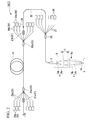
- FIG. 1 is a view schematically showing a laser materials processing apparatus 10 related to one embodiment of the present invention.
- the laser materials processing apparatus 10 of the present embodiment is generally constituted by a laser apparatus 1, an irradiation optical system 7, and a housing 8.
- the irradiation optical system 7 is constituted by, for example, a collimating lens 5 and a condenser lens 6.
- the collimating lens 5 and the condenser lens 6 are arranged within the housing 8 so as to be movable up and down independently from each other.
- An output end 3 (an output end 3 of a passive fiber 22) of the laser apparatus 1 is connected to the housing 8.
- Laser beams 4 (4a, 4b) emitted from the output end 3 of the passive fiber 22 are turned into parallel light in the collimating lens 5, are condensed with a suitable size by the condenser lens 6, and are irradiated to a workpiece 9.
- the laser materials processing apparatus 10 of the present embodiment is used, for example, when cutting, grooving, welding, or cladding of metals or the like is performed.
- the cutting or grooving is performed while oxygen gas or nitrogen gas is introduced as an assist gas from a gas inlet 8a formed in the housing 8.
- the assist gas introduced into the housing 8 is jetted from a tip opening 8b of the housing 8 to remove molten metal from a cutting curf.
- the welding or cladding is performed while inert gas, such as nitrogen gas or argon gas, is introduced into the housing 8 from the gas inlet 8a, and this inert gas is jetted from the tip opening 8b of the housing 8.
- inert gas such as nitrogen gas or argon gas
- the opening may have a coaxial multi-structure and a plurality of corresponding gas inlets may be provided.
- FIG. 2 is a view schematically showing the laser apparatus 1.
- a laser apparatus 1A(1) of the present embodiment is used as a laser oscillator of the laser materials processing apparatus 10.
- the laser apparatus 1A is generally constituted by a first laser oscillator, a passive fiber 22 that is a double-clad fiber that transmits a first laser beam emitted from the first laser oscillator through a core, and a second laser oscillator that emits a laser beam coupled into the inner cladding of the passive fiber 22.
- the first laser oscillator is generally constituted by an active fiber 20 that performs laser operation and is a double-clad fiber, fiber Bragg gratings (FBGs) 21 (21 a, 21 b) that are formed in the vicinity of both ends of the active fiber 20, first multi-couplers 23 (23 a, 23b) that are arranged inside the respective FBGs 21, a plurality of pumping light sources 26 (26a, 26b), and first optical fibers 25 (25a, 25b) that optically connects the first multi-couplers 23 (23a, 23b) and the pumping light sources 26 (26a, 26b).
- the passive fiber 22 that transmits the first laser beam is connected to the active fiber 20 via a connecting point 29.
- the second laser oscillator includes a plurality of semiconductor laser beam sources 28.
- a second multi-coupler 24 is arranged on the passive fiber 22, and the second multi-coupler 24 and the respective semiconductor laser beam sources 28 are optically connected by a plurality of second optical fibers 27.
- the active fiber 20 formed with the FBGs 21 (21a, 21b) acts as a laser resonator. That is, the FBG 21a is a total reflection mirror and the FBG 21b is a partial reflection mirror.
- the cores of the active fiber 20 and the passive fiber 22 are connected by fusion or the like at the connecting point 29.
- FIG. 3 is a view schematically showing the cross-section of the active fiber 20 used for the laser apparatus 1A of the present embodiment.
- the active fiber 20 is constituted by a core 20a, inner cladding 20b provided around the core 20a, and outer cladding 20c provided around the inner cladding 20b.
- the core 20a is made of, for example, quartz as a base material, and rare earth elements, such as ytterbium (Yb) or erbium (Er), are doped to quartz. Additionally, a dopant that enhances the refractive index of germanium (Ge), phosphorus (P), or the like may be added.
- the core 20a becomes a laser medium.
- the FBGs 21 are formed in the core 20a in the vicinity of both ends of the active fiber 20.
- the inner cladding 20b has a refractive index lower than the core 20a, and is formed from, for example, quartz to which fluorine (F) or boron (B) is added. In a case where Ge or P is added to the core 20a, the inner cladding may be formed only from quartz.
- Pumping light emitted from the pumping light sources 26 (26a, 26b) enters the inner cladding 20b via the first optical fiber 25 (25a, 25b) and the first multi-coupler 23 (23a, 23b), respectively, and performs optical pumping of the rare earth element of the core 20a.
- the cross-sectional shape of the inner cladding 20b may be a circular shape or may be a polygonal shape or a D-shape as long as the laser oscillation is allowed.
- the outer cladding 20c has a refractive index lower than the inner cladding 20b, and acts as cladding for the pumping light that is guided by the core 20a and the inner cladding 20b.
- the outer cladding 20c is formed from, for example, resin. Alternatively, the outer cladding may be made of quartz to which F, B, or the like is added.
- FIG. 2 will be referred to again.
- Semiconductor lasers are suitable as the pumping light sources 26 (26a, 26b).
- the number or output of the pumping light sources is not particularly limited and is appropriately set according to the output of a fiber laser beam required.
- the wavelength of the pumping light emitted from the respective pumping light sources 26 (26a, 26b) is matched with the absorption wavelength of the rare earth elements doped to the core 20a.
- the pumping light sources 26 constituted by semiconductor lasers are also referred to as first semiconductor laser beam sources 26.
- the first optical fibers 25 (25a, 25b) are not particularly limited if the pumping light can be guided, and ordinary single-clad fibers with single-layer cladding can be used as the first optical fibers.
- the passive fiber 22 has a double-clad structure including a core 22a, inner clad 22b provided around the core 22a, and outer clad 22c provided around the inner clad 22b, similarly to the active fiber 20.
- the passive fiber is different from the active fiber 20 in that the rare earth elements are not doped to the core 22a of the passive fiber 22 and the FBGs are not formed.
- the cross-sectional shape of the inner cladding 22b is preferably a circular shape. A fiber laser beam emitted from a core end face of the active fiber 20 is introduced into the core 22a of the passive fiber 22.
- Second laser beams Semiconductor laser beams (second laser beams) emitted from the semiconductor laser beam sources (also referred to as second semiconductor laser beam sources) 28 are coupled into the inner cladding 22b of the passive fiber 22 via the second optical fibers 27 and the second multi-coupler 24. That is, the two laser beams (the fiber laser beam 4a and the semiconductor laser beam 4b) are coupled to the passive fiber 22 and thereby coaxialized. For this reason, the coaxialization of the laser beams 4 (4a, 4b) can be performed simply rather than in a case where the two laser beams 4 (4a, 4b) are coaxialized using a mirror or the like and are stable against surrounding environmental changes (temperature change or the like), vibration, or the like.
- the fiber laser beam 4a and the semiconductor laser beam 4b that are coaxialized are emitted from the passive fiber 22, that is, the emitting end 3 of the laser apparatus 1A.
- These laser beams are irradiated to an irradiation point ⁇ via the irradiation optical system 7 including the collimating lens 5, the condenser lens 6, and the like.
- the core diameter of the passive fiber 22 is preferably equal to or larger than that of the active fiber 20.
- the refractive indexes of the inner clad 22b and the outer clad 22c of the passive fiber 22 may be the same as or different from the refractive index of the active fiber 20.
- the refractive indexes of the inner clad 22b and the outer clad 22c can be appropriately set depending on the wavelength of the semiconductor laser beam that is coupled into the inner clad 22b of the passive fiber 22.
- the number or output of the second semiconductor laser beam sources 28 is not particularly limited, and is appropriately set according to the output of the semiconductor laser beam 4b required.
- the wavelength of the semiconductor laser beams emitted from the second semiconductor laser beam sources 28 may be the same as or different from that of the pumping light sources 26 (26a, 26b) (first semiconductor laser beam sources).
- the second optical fibers 27 are not particularly limited if the semiconductor laser beams can be guided, and ordinary single-clad fibers with single-layer cladding can be used as the second optical fibers.
- FIG. 4 is a view schematically showing the situation that the fiber laser beam 4a and the semiconductor laser beam 4b are coupled into the passive fiber 22, and is a cross-sectional view of the passive fiber 22 cut in a plane including the axis of a fiber.
- ⁇ FL ⁇ LD be established regarding the incident angle ⁇ FL of the fiber laser beam 4a that is coupled into the core 22a and the incident angle ⁇ LD of the semiconductor laser beam 4b that is coupled into the inner clad 22b.
- the semiconductor laser beam 4b is automatically arranged outside the fiber laser beam 4a at a focusing point when being condensed by the same optical system.
- the refractive indexes of the core 22a and the inner clad 22b of the passive fiber 22 may be adjusted to suitable values. That is, ⁇ FL ⁇ LD is obtained by setting the relative index difference ⁇ between the core 22a and the inner clad 22b to ⁇ >0.
- the relative index difference ⁇ is defined by ⁇ (n1-n2)/n1 when the refractive index of the core 22a is n1 and the refractive index of the inner clad 22b is n2.
- FIG. 5 is a view showing the power density distribution of the laser beams 4 (4a, 4b) at the irradiation point ⁇ (obtained by the laser apparatus 1A of the present embodiment), X represents the distance from the center O of the laser beams 4 at the irradiation point ⁇ and I represents the magnitude of the power density of the laser beams 4.
- the fiber laser beam 4a emitted from the laser resonator (active fiber 20) and the semiconductor laser beam 4b emitted from the semiconductor laser beam sources 28 are irradiated to the irradiation point ⁇ . Therefore, as shown in FIG.
- the s power density distribution at the irradiation point ⁇ has a substantially uniform top-hat shape.
- the power density I a of the fiber laser beam 4a and the power density I b of the semiconductor laser beam 4b are preferably I a >I b and more preferably I a /10 ⁇ I b .
- the power density I a of the fiber laser beam 4a at the irradiation point ⁇ is obtained by dividing the output P a (W) of the fiber laser beam 4a by spot area S a (mm 2 ) because the distribution of this laser beam is uniform, that is, top-hat shaped. That is, the power density I a of the fiber laser beam 4a is obtained by the following Formula (2).
- the power density I b of the semiconductor laser beam 4b at the irradiation point ⁇ is obtained by dividing the power P b (W) of the semiconductor laser beam 4b by spot area S b (mm 2 ). That is, the power density I b of the semiconductor laser beam 4b is obtained by the following Formula (3).
- the spot diameter D1 of the fiber laser beam 4a and the spot diameter D2 of the semiconductor laser beam 4b at the irradiation point ⁇ are expressed by the following Formulas (4) and (5), respectively.
- d1 (mm) is the core diameter of the passive fiber 22 that transmits the fiber laser beam 4a
- d2 (mm) is the diameter of the inner cladding of the passive fiber 22 that transmits the semiconductor laser beam 4b.
- the above-identified “fa” is the focal length (mm) of the collimating lens 5
- the above-identified “fb” is the focal length (mm) of the condenser lens 6.
- the fiber laser beam 4a propagates through only the core 22a of the passive fiber 22. Accordingly, the diameter of the fiber laser beam 4a at an outlet of the passive fiber 22 is given by the core diameter d1 of the passive fiber 22.
- the semiconductor laser beam 4b spreads and propagates also through the inner cladding 22b in addition to the core 22a of the passive fiber 22. Accordingly, the diameter of the semiconductor laser beam 4b at the outlet of the passive fiber 22 is given by the diameter d2 of the inner cladding 22b of the passive fiber 22.
- the spot diameters of the laser beams 4a and 4b become D1 ⁇ D2 (the semiconductor laser beam 4b becomes larger).
- a form as shown in FIG. 5 is obtained in which a skirt formed by the semiconductor laser beam 4b is added to the periphery of an overlapping component between the fiber laser beam 4a and the semiconductor laser beam 4b. Accordingly, when the workpiece 9 is processed while the laser beam 4 is moved, the semiconductor laser beam 4b is irradiated to a part to be processed ahead of the overlapping component between the fiber laser beam 4a and the semiconductor laser beam 4b. Accordingly, processing is performed by the overlapping component between the fiber laser beam 4a and the semiconductor laser beam 4b after a part to be processed is sufficiently preheated by the semiconductor laser beam 4b.
- the two laser beams 4a and 4b are emitted from different light sources, respectively. Therefore, the power densities I a and I b of the respective laser beams 4a and 4b can be independently adjusted. Additionally, the spot diameters D1 and D2 of the respective laser beams 4a and 4b can be adjusted by changing the diameters of the cores 20a and 22a or the diameters of the inner cladding 20b and 22b in the active fiber 20 and the passive fiber 22. Accordingly, in the present embodiment, the two laser beams 4a and 4b can be easily optimized to configurations suitable for respective processing.
- the central wavelength ⁇ 1 of the fiber laser beam 4a is preferably different from the central wavelength ⁇ 2 of the semiconductor laser beam 4b. That is, ⁇ 2/ ⁇ 1 is preferably about 0.6 to 0.97. This can suppress the chromatic aberration between the fiber laser beam 4a and the semiconductor laser beam 4b at the irradiation point ⁇ . As a result, the workpiece 9 can be processed with stable power density.
- FIG. 6 is a view schematically illustrating a mechanism of the laser cutting, and showing a cross-section in a plane including a laser beam and cutting line.
- Laser cutting is roughly divided into the processes that includes a heating and melting of a cutting front 72 by the laser beam 71, and a removal of a melting layer 73 by an assist gas flow 74.
- FIG. 6 shows the situation of a specific moment in time under cutting, and the cutting process progresses every moment to the left of FIG. 6 as shown by arrow 75.
- cutting using the laser apparatus of the related art has a problem in that the roughness of a cutting surface deteriorates compared to a case where CO 2 laser is used. This problem becomes marked, particularly in a case where the workpiece 70 is thick or when the workpiece is cut at a low speed.
- V 0 I 0 ⁇ ⁇ C p ⁇ T m
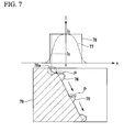
- FIG. 7 is a view schematically showing a situation in which deterioration of the cutting surface roughness occurs at V ⁇ V 0 , using the laser apparatus of the related art.
- V ⁇ V 0 a melting phenomenon becomes discontinuous in the vicinity 79a of the surface of the workpiece 79, and regions P (convex portions 76) where the absorption power density of a laser beam is high appear locally in a curf front. This causes deterioration of the surface roughness.
- the relationship between the position of a laser beam and the position where the surface temperature T of the workpiece 79 reaches T m is also shown in FIG. 7 .
- the power density distribution 77 (Gaussian shape) of a CO 2 laser beam and the power density distribution 78 (top-hat shape) of a fiber laser beam are simultaneously shown for convenience in FIG. 7 .
- the CO 2 laser beam with the Gaussian distribution has a smaller value of I 0 than that of the fiber laser beam with the top-hat shaped distribution. Accordingly, in a case where the laser apparatus of the related art is used, I 0 described in the above Formula (6) becomes large, and the range of speed where deterioration of the cutting surface roughness occurs becomes wider than that in the case where CO 2 laser is used.
- the semiconductor laser beam 4b having the power density I b is first irradiated to the workpiece. Therefore, the workpiece ahead of the cutting location can be preheated. In this case, the energy absorption of the fiber laser beam 4b occurs in the preheated location. In the present embodiment, I a >I b is established, therefore, this energy absorption did not occur excessively, and the value of I 0 can be made smaller than the laser apparatus of the related art similarly to the case where CO 2 laser is used. Therefore, cutting of the workpiece is allowed at a wider range speed while suppressing deterioration of the cutting surface roughness.
- the power density I b of the semiconductor laser beam 4b preferably satisfies the following Formula (7). This allows cutting of the workpiece 9 while suppressing deterioration of the cutting surface roughness even in a case where processing speed is low or a case where the workpiece 9 is thick.
- I b satisfies the following Formula (7), and for example, SUS304 is used as the workpiece 9, cutting using the laser beam 4 under the conditions that the thickness of the workpiece 9 is 4 to 12 mm, the cutting speed is 0.5 to 3 m per minute (mpm), and the cutting surface roughness is equal to or less than about 30 ⁇ m or less is allowed.
- I b ⁇ (D2-D1)/2 correspond to the area (the integration value of the power density of one region 42a of the second region 42 outside the first region, in the power density distribution of the semiconductor laser beam 4b) of a shaded portion 42a of FIG. 5 .
- A represents the absorption factor of the semiconductor laser beam 4b to the workpiece 9
- ⁇ represents the thermal diffusion coefficient of the workpiece 9
- ⁇ represents the density of the workpiece 9
- C p represents the specific heat of the workpiece 9
- T m represents the melting point of the workpiece 9
- T 0 represents the initial temperature (room temperature) of the workpiece 9
- L m represents the latent heat of fusion of the workpiece 9.
- the same can also be applicable regarding a case where grooving processing is performed to the workpiece 9.
- the laser apparatus 1A and the fiber processing apparatus 10 of the embodiment By using the laser apparatus 1A and the fiber processing apparatus 10 of the embodiment, grooving processing at a wider range speed is allowed, and the roughness of a formed groove is improved.
- the laser apparatus 1A and the laser materials processing apparatus 10 of the present embodiment can also be applied to welding or cladding. In welding or cladding using the laser apparatus of the related art, there is a case where the amount of spatteing matter of a workpiece may increase as compared to the processing using CO 2 laser, and this processing cannot be performed with desired quality. This phenomenon becomes marked particularly in a case where the processing speed is slow.
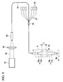
- FIG. 8 schematically shows a modified example of the laser apparatus of the present invention.
- the laser apparatus 1B(1) is different from the above-described laser apparatus 1A(1) in that the first laser beam 52 emitted from the first laser oscillator 51 is condensed by the lens 53 and is coupled into the passive fiber 22 from the incident end 54.
- This laser apparatus 1C(1) is different from the above-described laser apparatus 1A(1) in that the first laser beam 52 emitted from the first laser oscillator 51 is condensed by the lens 53 and is coupled into the ordinary optical fiber 55 with single-layer cladding from the incident end 54, and the passive fiber 22 is connected to the downstream side of the optical fiber 55.
- the first laser beam incident on the passive fiber 22 propagates through the core 22a of the fiber 22.
- the semiconductor laser beams emitted from the second semiconductor laser beam sources 28 as second laser oscillators are coupled into the inner cladding 22b of the passive fiber 22 via the optical fiber 27 and the second multi-coupler 24. In this way, the first laser beam and the semiconductor laser beams are coupled to the passive fiber 22 and thereby coaxialized.
- the same effects as those described above can be obtained by making the power density I b of semiconductor laser beam smaller than the power density I a of the first laser beam emitted from the first laser oscillator.
- the first laser oscillator for example, a disk laser can be used.
- Example 1 of the present invention the laser apparatus 1A shown in FIG. 2 was assembled, and the laser materials processing apparatus 10 shown in FIG. 1 was assembled using this laser apparatus.
- the wavelength of signal light was 1085 nm, and the wavelength of pumping light and a semiconductor laser beam was 976 nm.
- As the active fiber a double cladding fiber in which the core diameter is 0.2 mm, the diameter of the inner cladding is 0.8 mm, and Yb that is doped on the core was used.
- the passive fiber a double-clad fiber in which the core diameter is 0.2 mm, the diameter of the inner cladding is 0.8 mm, without a rare earth element doping to the core, was used.
- the relative index difference between the core and the inner cladding was 0.002.
- the maximum output obtained from the output end of the laser apparatus 1A was 4 kW in the fiber laser beam with a wavelength of 1085 nm and was 2 kW in the semiconductor laser beam with a wavelength of 976 nm.
- the output of the fiber laser beam was fixed to 4 kW, and the output of the semiconductor laser beam was appropriately changed.
- Example 1 In the comparative example (equivalent to a conventional example), the output of the semiconductor laser beam in Example 1 was set to zero.
- SUS304 was cut by the laser materials processing apparatuses of Example 1 and the comparative example, using nitrogen gas as the assist gas.
- the thickness of the SUS304 was kept constant at 10 mm, and the cutting speed was kept constant at 1 (mpm).
- the cutting surface roughness the roughness in the direction of a cutting line at a depth of 1 mm from the surface of a material was measured.
- SUS304 was cut while changing the output (P2) of the semiconductor laser beam, and the cutting surface roughness (Rz) was investigated. The results are shown in Table 1 and FIG. 10 .
- P2 is the output (W) of the semiconductor laser beam
- I b is the power density (W/m 2 ) of the semiconductor laser beam
- Rz is the average of measured cutting surface roughness ( ⁇ m).
- the cutting surface roughness Rz was 53.6 ⁇ m.
- the cutting surface roughness Rz decreased as compared to the comparative example.
- the output (P2) of the semiconductor laser beam was raised, the cutting surface roughness Rz decreased. If P2 becomes equal to or more than 50W, that is, the left side I b ⁇ (D2-D1)/2 of the above Formula (7) becomes equal to or more than 3.0x10 4 (W/m), it turns out that a great effect for smoothing of a cutting surface is exhibited.
- the value of the right side 0.2 ⁇ (1/A) ⁇ C p (T m -T 0 )+ ⁇ L m ⁇ described in the above Formula (7) is 2.8x10 4 (W/m). Accordingly, it turns out that the condition that the effect is further exhibiting is a range described in the above Formula (7).
- Example 2 Comparative Example Plate Thickness (mm) V (mpm) P2 (W) Rz ( ⁇ m) Plate Thickness (mm) V (mpm) P2 (W) Rz ( ⁇ m) 1 15 1800 17.3 1 15 0 18.6 2 7 1500 19.5 2 7 0 22.3 4 3 1300 22.0 4 3 0 26.9 6 2 1200 26.8 6 2 0 35.4 8 1.4 1100 27.8 8 1.4 0 44.1 10 1 1000 31.6 10 1 0 53.6 12 0.7 800 33.4 12 0.7 0 60.7
- the cutting surface roughness Rz deteriorated as the plate thickness became larger, that is, the cutting speed became lower.
- the value of the cutting surface roughness Rz was small, and deterioration of the cutting surface roughness was suppressed.
- the plate thickness was larger and the cutting speed was slower, deterioration of the cutting surface roughness Rz was more effectively suppressed.
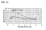
- Example 3 Comparative Example V (mpm) P2 (W) Mass Reduction (g) V (mpm) P2 (W) Mass Reduction (g) 0.7 800 0.36 0.7 0 0.69 1 1000 0.35 1 0 0.65 2 1200 0.31 2 0 0.53 3 1300 0.25 3 0 0.37 4 1350 0.25 4 0 0.29 5 1400 0.23 5 0 0.25
- Example 3 In the comparative example, as the welding speed was slow, the amount of reduction in the mass increased. In contrast, in Example 3, reduction in the mass at every welding speed was suppressed more than that of the comparative example. That is, reduction in the amount of spattering matter generated during welding of the workpiece (steel) was observed. Accordingly, the method of Example 3 also has an effect of suppressing adhesion of the spatters of welding or suppressing depressions of beads.
Landscapes
- Physics & Mathematics (AREA)
- Electromagnetism (AREA)
- Optics & Photonics (AREA)
- Engineering & Computer Science (AREA)
- Plasma & Fusion (AREA)
- Mechanical Engineering (AREA)
- Laser Beam Processing (AREA)
- Lasers (AREA)
Applications Claiming Priority (1)
| Application Number | Priority Date | Filing Date | Title |
|---|---|---|---|
| PCT/JP2010/068270 WO2012053045A1 (fr) | 2010-10-18 | 2010-10-18 | Appareil laser et appareil de traitement laser équipé de celui-ci |
Publications (3)
| Publication Number | Publication Date |
|---|---|
| EP2631999A1 true EP2631999A1 (fr) | 2013-08-28 |
| EP2631999A4 EP2631999A4 (fr) | 2014-05-07 |
| EP2631999B1 EP2631999B1 (fr) | 2015-09-16 |
Family
ID=45974783
Family Applications (1)
| Application Number | Title | Priority Date | Filing Date |
|---|---|---|---|
| EP10858601.7A Not-in-force EP2631999B1 (fr) | 2010-10-18 | 2010-10-18 | Appareil laser et appareil de traitement laser équipé de celui-ci |
Country Status (5)
| Country | Link |
|---|---|
| US (1) | US9172202B2 (fr) |
| EP (1) | EP2631999B1 (fr) |
| JP (1) | JP5360305B2 (fr) |
| CN (1) | CN103155308B (fr) |
| WO (1) | WO2012053045A1 (fr) |
Cited By (1)
| Publication number | Priority date | Publication date | Assignee | Title |
|---|---|---|---|---|
| US12228002B1 (en) | 2023-09-14 | 2025-02-18 | Saudi Arabian Oil Company | Laser cladding downhole repair |
Families Citing this family (28)
| Publication number | Priority date | Publication date | Assignee | Title |
|---|---|---|---|---|
| US20150266134A1 (en) * | 2012-10-26 | 2015-09-24 | Komatsu Industries Corporation | Fiber laser processing machine, fiber connection method and fiber laser oscillator |
| JP6027461B2 (ja) * | 2013-02-27 | 2016-11-16 | 鈴木電機工業株式会社 | 肉盛り加工装置 |
| US10286487B2 (en) | 2013-02-28 | 2019-05-14 | Ipg Photonics Corporation | Laser system and method for processing sapphire |
| US10537965B2 (en) | 2013-12-13 | 2020-01-21 | Applied Materials, Inc. | Fiber array line generator |
| US9764427B2 (en) * | 2014-02-28 | 2017-09-19 | Ipg Photonics Corporation | Multi-laser system and method for cutting and post-cut processing hard dielectric materials |
| US9956646B2 (en) | 2014-02-28 | 2018-05-01 | Ipg Photonics Corporation | Multiple-beam laser processing using multiple laser beams with distinct wavelengths and/or pulse durations |
| US10343237B2 (en) | 2014-02-28 | 2019-07-09 | Ipg Photonics Corporation | System and method for laser beveling and/or polishing |
| JP2015196163A (ja) * | 2014-03-31 | 2015-11-09 | 三菱重工業株式会社 | 加工装置及び加工方法 |
| CN107148324A (zh) | 2014-08-28 | 2017-09-08 | Ipg光子公司 | 用于切割和切割后加工硬质电介质材料的多激光器系统和方法 |
| WO2016033494A1 (fr) | 2014-08-28 | 2016-03-03 | Ipg Photonics Corporation | Systeme et procede de biseautage et/ou de polissage par laser |
| US9397464B2 (en) * | 2014-12-19 | 2016-07-19 | Lumentum Operations Llc | Fiber laser assembly and method of generating light |
| DE102015103127A1 (de) * | 2015-03-04 | 2016-09-08 | Trumpf Laser- Und Systemtechnik Gmbh | Bestrahlungssystem für eine Vorrichtung zur generativen Fertigung |
| CN105397308B (zh) * | 2015-12-18 | 2017-05-17 | 张飞 | 一种多功能打标机 |
| WO2017136831A1 (fr) * | 2016-02-05 | 2017-08-10 | Nufern | Fibres optiques à mélange de modes et procédés et systèmes utilisant celles-ci |
| JP2017194514A (ja) * | 2016-04-19 | 2017-10-26 | 株式会社フジクラ | 光部品、ファイバレーザユニット、およびファイバレーザシステム |
| JP6937865B2 (ja) * | 2016-09-20 | 2021-09-22 | 株式会社アマダ | ダイレクトダイオードレーザ加工装置及びこれを用いた板金の加工方法 |
| JP2016221579A (ja) * | 2016-09-20 | 2016-12-28 | 株式会社アマダホールディングス | ダイレクトダイオードレーザ加工装置及びこれを用いた板金の加工方法 |
| JP6870974B2 (ja) * | 2016-12-08 | 2021-05-12 | 株式会社ディスコ | 被加工物の分割方法 |
| JP6938212B2 (ja) | 2017-05-11 | 2021-09-22 | 株式会社ディスコ | 加工方法 |
| DE102018204814B4 (de) | 2018-03-29 | 2025-03-06 | TRUMPF Werkzeugmaschinen SE + Co. KG | Vorrichtung und Verfahren zum Erzeugen von Laserstrahlungen mit unterschiedlicher Leistung und Brillanz |
| JP2019193944A (ja) * | 2018-05-01 | 2019-11-07 | 株式会社島津製作所 | レーザ加工装置 |
| WO2021145205A1 (fr) * | 2020-01-15 | 2021-07-22 | パナソニックIpマネジメント株式会社 | Dispositif laser et dispositif de traitement laser dans lequel celui-ci est utilisé |
| WO2021157546A1 (fr) * | 2020-02-05 | 2021-08-12 | パナソニックIpマネジメント株式会社 | Appareil de traitement laser |
| DE102020205948A1 (de) * | 2020-05-12 | 2021-11-18 | Trumpf Laser- Und Systemtechnik Gmbh | Laserschneidverfahren und Laserschneidanlage |
| CN113794091B (zh) * | 2020-05-25 | 2023-07-18 | 深圳市创鑫激光股份有限公司 | 一种激光器和多波长输出激光加工系统 |
| JP2021191588A (ja) * | 2020-06-04 | 2021-12-16 | 古河電気工業株式会社 | レーザ切断方法およびレーザ切断装置 |
| US20220009027A1 (en) * | 2020-07-07 | 2022-01-13 | Panasonic Intellectual Property Management Co. Ltd | Step-core fiber structures and methods for altering beam shape and intensity |
| CN116104510B (zh) * | 2022-09-14 | 2026-04-21 | 深圳大学 | 一种表面激光致裂辅助破岩设备 |
Family Cites Families (17)
| Publication number | Priority date | Publication date | Assignee | Title |
|---|---|---|---|---|
| JPS58159514A (ja) * | 1982-03-18 | 1983-09-21 | Toshiba Corp | レ−ザビ−ム空間分布形成方法 |
| JP2688303B2 (ja) | 1992-03-24 | 1997-12-10 | 日本電信電話株式会社 | ファイバレーザおよびファイバ増幅器 |
| US6477295B1 (en) * | 1997-01-16 | 2002-11-05 | Jds Uniphase Corporation | Pump coupling of double clad fibers |
| US6275250B1 (en) * | 1998-05-26 | 2001-08-14 | Sdl, Inc. | Fiber gain medium marking system pumped or seeded by a modulated laser diode source and method of energy control |
| US6529318B1 (en) * | 2001-08-30 | 2003-03-04 | Np Photonics, Inc. | Total internal reflection (TIR) coupler and method for side-coupling pump light into a fiber |
| US6836356B2 (en) | 2002-04-18 | 2004-12-28 | Np Photonics, Inc. | Alkali-metal-free phosphate glass with dn/dT ≈ 0 for use in fiber amplifiers |
| JP2004154813A (ja) | 2002-11-06 | 2004-06-03 | National Institute Of Advanced Industrial & Technology | レーザ加工方法および装置 |
| JP2004337881A (ja) | 2003-05-13 | 2004-12-02 | Matsushita Electric Ind Co Ltd | レーザ加工方法およびレーザ加工装置 |
| US7403674B2 (en) * | 2003-07-18 | 2008-07-22 | Network Integrity Systems Inc. | Intrusion detection system for a multimode optical fiber using a bulk optical wavelength division multiplexer for maintaining modal power distribution |
| JP2005084386A (ja) | 2003-09-09 | 2005-03-31 | Mitsubishi Cable Ind Ltd | ダブルクラッドファイバ及びそれを備えた光学装置、並びに、光増幅器 |
| JP2007190566A (ja) * | 2006-01-17 | 2007-08-02 | Miyachi Technos Corp | ファイバレーザ加工装置 |
| US7768700B1 (en) * | 2006-11-30 | 2010-08-03 | Lockheed Martin Corporation | Method and apparatus for optical gain fiber having segments of differing core sizes |
| JP4784406B2 (ja) * | 2006-06-13 | 2011-10-05 | 住友電気工業株式会社 | ファイバレーザ装置およびレーザ加工方法 |
| US7483607B2 (en) | 2006-11-07 | 2009-01-27 | Synergetics, Inc. | Dual core optic fiber illuminated laser probe |
| CN101212115A (zh) | 2006-12-28 | 2008-07-02 | 中国科学院半导体研究所 | 可调谐掺铒光纤环形腔激光器 |
| CN101615761B (zh) | 2008-06-24 | 2011-02-16 | 中国科学院西安光学精密机械研究所 | 相干组束全光纤激光器 |
| CN101340053A (zh) | 2008-08-13 | 2009-01-07 | 中国科学院上海光学精密机械研究所 | 中红外掺铥光纤激光放大器 |
-
2010
- 2010-10-18 JP JP2012539486A patent/JP5360305B2/ja active Active
- 2010-10-18 WO PCT/JP2010/068270 patent/WO2012053045A1/fr not_active Ceased
- 2010-10-18 EP EP10858601.7A patent/EP2631999B1/fr not_active Not-in-force
- 2010-10-18 US US13/879,528 patent/US9172202B2/en not_active Expired - Fee Related
- 2010-10-18 CN CN201080069641.2A patent/CN103155308B/zh not_active Expired - Fee Related
Cited By (1)
| Publication number | Priority date | Publication date | Assignee | Title |
|---|---|---|---|---|
| US12228002B1 (en) | 2023-09-14 | 2025-02-18 | Saudi Arabian Oil Company | Laser cladding downhole repair |
Also Published As
| Publication number | Publication date |
|---|---|
| JPWO2012053045A1 (ja) | 2014-02-24 |
| EP2631999A4 (fr) | 2014-05-07 |
| CN103155308A (zh) | 2013-06-12 |
| EP2631999B1 (fr) | 2015-09-16 |
| US9172202B2 (en) | 2015-10-27 |
| WO2012053045A1 (fr) | 2012-04-26 |
| JP5360305B2 (ja) | 2013-12-04 |
| CN103155308B (zh) | 2016-06-01 |
| US20130215914A1 (en) | 2013-08-22 |
Similar Documents
| Publication | Publication Date | Title |
|---|---|---|
| EP2631999B1 (fr) | Appareil laser et appareil de traitement laser équipé de celui-ci | |
| US12447553B2 (en) | Laser processing apparatus and method | |
| CN107850726B (zh) | 激光加工装置和方法以及因此的光学部件 | |
| US7592568B2 (en) | Apparatus for the industrial processing of a material by optical radiation | |
| EP3465301B1 (fr) | Dispositif à fibre optique | |
| JP5496370B2 (ja) | 光ファイバ、及びそれを備えたレーザ加工装置 | |
| US20120024831A1 (en) | Method for Cutting Stainless Steel with a Fiber Laser | |
| CN102149508A (zh) | 利用通过衍射光学部件修改激光束品质因子的装置的激光切割方法和设备 | |
| WO2012165389A1 (fr) | Dispositif laser et dispositif d'usinage | |
| CN102197550B (zh) | 掺镱光纤 | |
| US20220037847A1 (en) | Optical fiber for a fiber laser, fiber laser, and production method for optical fiber for a fiber laser | |
| WO2019150064A1 (fr) | Appareil et procédé de commande du profil spatial de faisceaux de rayonnement laser | |
| JP6578016B2 (ja) | 光ファイバ設計方法 | |
| CN114072712A (zh) | 光合并器、激光装置、以及光合并器的制造方法 | |
| EP3613113B1 (fr) | Laser raman à fibre monomode pompée à gainage haute puissance | |
| JP7703366B2 (ja) | レーザ加工装置およびレーザ加工方法 | |
| JP6628777B2 (ja) | 反射鏡、ファイバ共振器、およびファイバレーザ | |
| Xiao | Fiber laser cutting of mild steel | |
| US9535212B1 (en) | Single mode large mode area optical fiber coil | |
| Kashiwagi et al. | High power single-mode fiber laser and a multi-mode delivery cable |
Legal Events
| Date | Code | Title | Description |
|---|---|---|---|
| PUAI | Public reference made under article 153(3) epc to a published international application that has entered the european phase |
Free format text: ORIGINAL CODE: 0009012 |
|
| 17P | Request for examination filed |
Effective date: 20130515 |
|
| AK | Designated contracting states |
Kind code of ref document: A1 Designated state(s): AL AT BE BG CH CY CZ DE DK EE ES FI FR GB GR HR HU IE IS IT LI LT LU LV MC MK MT NL NO PL PT RO RS SE SI SK SM TR |
|
| DAX | Request for extension of the european patent (deleted) | ||
| A4 | Supplementary search report drawn up and despatched |
Effective date: 20140409 |
|
| RIC1 | Information provided on ipc code assigned before grant |
Ipc: B23K 26/06 20140101AFI20140403BHEP Ipc: H01S 3/00 20060101ALN20140403BHEP |
|
| REG | Reference to a national code |
Ref country code: DE Ref legal event code: R079 Ref document number: 602010027644 Country of ref document: DE Free format text: PREVIOUS MAIN CLASS: H01S0003100000 Ipc: B23K0026060000 |
|
| RIC1 | Information provided on ipc code assigned before grant |
Ipc: H01S 3/094 20060101ALI20150209BHEP Ipc: H01S 3/23 20060101ALI20150209BHEP Ipc: H01S 3/067 20060101ALI20150209BHEP Ipc: B23K 26/06 20140101AFI20150209BHEP |
|
| GRAP | Despatch of communication of intention to grant a patent |
Free format text: ORIGINAL CODE: EPIDOSNIGR1 |
|
| INTG | Intention to grant announced |
Effective date: 20150323 |
|
| GRAS | Grant fee paid |
Free format text: ORIGINAL CODE: EPIDOSNIGR3 |
|
| GRAA | (expected) grant |
Free format text: ORIGINAL CODE: 0009210 |
|
| AK | Designated contracting states |
Kind code of ref document: B1 Designated state(s): AL AT BE BG CH CY CZ DE DK EE ES FI FR GB GR HR HU IE IS IT LI LT LU LV MC MK MT NL NO PL PT RO RS SE SI SK SM TR |
|
| REG | Reference to a national code |
Ref country code: GB Ref legal event code: FG4D |
|
| REG | Reference to a national code |
Ref country code: CH Ref legal event code: EP |
|
| REG | Reference to a national code |
Ref country code: IE Ref legal event code: FG4D |
|
| REG | Reference to a national code |
Ref country code: AT Ref legal event code: REF Ref document number: 749392 Country of ref document: AT Kind code of ref document: T Effective date: 20151015 |
|
| REG | Reference to a national code |
Ref country code: DE Ref legal event code: R096 Ref document number: 602010027644 Country of ref document: DE |
|
| REG | Reference to a national code |
Ref country code: NL Ref legal event code: MP Effective date: 20150916 |
|
| PG25 | Lapsed in a contracting state [announced via postgrant information from national office to epo] |
Ref country code: GR Free format text: LAPSE BECAUSE OF FAILURE TO SUBMIT A TRANSLATION OF THE DESCRIPTION OR TO PAY THE FEE WITHIN THE PRESCRIBED TIME-LIMIT Effective date: 20151217 Ref country code: NO Free format text: LAPSE BECAUSE OF FAILURE TO SUBMIT A TRANSLATION OF THE DESCRIPTION OR TO PAY THE FEE WITHIN THE PRESCRIBED TIME-LIMIT Effective date: 20151216 Ref country code: FI Free format text: LAPSE BECAUSE OF FAILURE TO SUBMIT A TRANSLATION OF THE DESCRIPTION OR TO PAY THE FEE WITHIN THE PRESCRIBED TIME-LIMIT Effective date: 20150916 Ref country code: LT Free format text: LAPSE BECAUSE OF FAILURE TO SUBMIT A TRANSLATION OF THE DESCRIPTION OR TO PAY THE FEE WITHIN THE PRESCRIBED TIME-LIMIT Effective date: 20150916 Ref country code: LV Free format text: LAPSE BECAUSE OF FAILURE TO SUBMIT A TRANSLATION OF THE DESCRIPTION OR TO PAY THE FEE WITHIN THE PRESCRIBED TIME-LIMIT Effective date: 20150916 |
|
| REG | Reference to a national code |
Ref country code: LT Ref legal event code: MG4D |
|
| REG | Reference to a national code |
Ref country code: AT Ref legal event code: MK05 Ref document number: 749392 Country of ref document: AT Kind code of ref document: T Effective date: 20150916 |
|
| PG25 | Lapsed in a contracting state [announced via postgrant information from national office to epo] |
Ref country code: RS Free format text: LAPSE BECAUSE OF FAILURE TO SUBMIT A TRANSLATION OF THE DESCRIPTION OR TO PAY THE FEE WITHIN THE PRESCRIBED TIME-LIMIT Effective date: 20150916 Ref country code: HR Free format text: LAPSE BECAUSE OF FAILURE TO SUBMIT A TRANSLATION OF THE DESCRIPTION OR TO PAY THE FEE WITHIN THE PRESCRIBED TIME-LIMIT Effective date: 20150916 Ref country code: SE Free format text: LAPSE BECAUSE OF FAILURE TO SUBMIT A TRANSLATION OF THE DESCRIPTION OR TO PAY THE FEE WITHIN THE PRESCRIBED TIME-LIMIT Effective date: 20150916 |
|
| PG25 | Lapsed in a contracting state [announced via postgrant information from national office to epo] |
Ref country code: NL Free format text: LAPSE BECAUSE OF FAILURE TO SUBMIT A TRANSLATION OF THE DESCRIPTION OR TO PAY THE FEE WITHIN THE PRESCRIBED TIME-LIMIT Effective date: 20150916 |
|
| PG25 | Lapsed in a contracting state [announced via postgrant information from national office to epo] |
Ref country code: ES Free format text: LAPSE BECAUSE OF FAILURE TO SUBMIT A TRANSLATION OF THE DESCRIPTION OR TO PAY THE FEE WITHIN THE PRESCRIBED TIME-LIMIT Effective date: 20150916 Ref country code: IS Free format text: LAPSE BECAUSE OF FAILURE TO SUBMIT A TRANSLATION OF THE DESCRIPTION OR TO PAY THE FEE WITHIN THE PRESCRIBED TIME-LIMIT Effective date: 20160116 Ref country code: IT Free format text: LAPSE BECAUSE OF FAILURE TO SUBMIT A TRANSLATION OF THE DESCRIPTION OR TO PAY THE FEE WITHIN THE PRESCRIBED TIME-LIMIT Effective date: 20150916 Ref country code: CZ Free format text: LAPSE BECAUSE OF FAILURE TO SUBMIT A TRANSLATION OF THE DESCRIPTION OR TO PAY THE FEE WITHIN THE PRESCRIBED TIME-LIMIT Effective date: 20150916 Ref country code: EE Free format text: LAPSE BECAUSE OF FAILURE TO SUBMIT A TRANSLATION OF THE DESCRIPTION OR TO PAY THE FEE WITHIN THE PRESCRIBED TIME-LIMIT Effective date: 20150916 Ref country code: SK Free format text: LAPSE BECAUSE OF FAILURE TO SUBMIT A TRANSLATION OF THE DESCRIPTION OR TO PAY THE FEE WITHIN THE PRESCRIBED TIME-LIMIT Effective date: 20150916 |
|
| PG25 | Lapsed in a contracting state [announced via postgrant information from national office to epo] |
Ref country code: AT Free format text: LAPSE BECAUSE OF FAILURE TO SUBMIT A TRANSLATION OF THE DESCRIPTION OR TO PAY THE FEE WITHIN THE PRESCRIBED TIME-LIMIT Effective date: 20150916 Ref country code: RO Free format text: LAPSE BECAUSE OF FAILURE TO SUBMIT A TRANSLATION OF THE DESCRIPTION OR TO PAY THE FEE WITHIN THE PRESCRIBED TIME-LIMIT Effective date: 20150916 Ref country code: PL Free format text: LAPSE BECAUSE OF FAILURE TO SUBMIT A TRANSLATION OF THE DESCRIPTION OR TO PAY THE FEE WITHIN THE PRESCRIBED TIME-LIMIT Effective date: 20150916 Ref country code: PT Free format text: LAPSE BECAUSE OF FAILURE TO SUBMIT A TRANSLATION OF THE DESCRIPTION OR TO PAY THE FEE WITHIN THE PRESCRIBED TIME-LIMIT Effective date: 20160118 |
|
| REG | Reference to a national code |
Ref country code: CH Ref legal event code: PL |
|
| REG | Reference to a national code |
Ref country code: DE Ref legal event code: R097 Ref document number: 602010027644 Country of ref document: DE |
|
| PG25 | Lapsed in a contracting state [announced via postgrant information from national office to epo] |
Ref country code: MC Free format text: LAPSE BECAUSE OF FAILURE TO SUBMIT A TRANSLATION OF THE DESCRIPTION OR TO PAY THE FEE WITHIN THE PRESCRIBED TIME-LIMIT Effective date: 20150916 |
|
| PLBE | No opposition filed within time limit |
Free format text: ORIGINAL CODE: 0009261 |
|
| STAA | Information on the status of an ep patent application or granted ep patent |
Free format text: STATUS: NO OPPOSITION FILED WITHIN TIME LIMIT |
|
| REG | Reference to a national code |
Ref country code: IE Ref legal event code: MM4A |
|
| PG25 | Lapsed in a contracting state [announced via postgrant information from national office to epo] |
Ref country code: CH Free format text: LAPSE BECAUSE OF NON-PAYMENT OF DUE FEES Effective date: 20151031 Ref country code: LI Free format text: LAPSE BECAUSE OF NON-PAYMENT OF DUE FEES Effective date: 20151031 |
|
| REG | Reference to a national code |
Ref country code: FR Ref legal event code: ST Effective date: 20160630 |
|
| 26N | No opposition filed |
Effective date: 20160617 |
|
| GBPC | Gb: european patent ceased through non-payment of renewal fee |
Effective date: 20151216 |
|
| PG25 | Lapsed in a contracting state [announced via postgrant information from national office to epo] |
Ref country code: FR Free format text: LAPSE BECAUSE OF NON-PAYMENT OF DUE FEES Effective date: 20151116 Ref country code: DK Free format text: LAPSE BECAUSE OF FAILURE TO SUBMIT A TRANSLATION OF THE DESCRIPTION OR TO PAY THE FEE WITHIN THE PRESCRIBED TIME-LIMIT Effective date: 20150916 |
|
| PG25 | Lapsed in a contracting state [announced via postgrant information from national office to epo] |
Ref country code: IE Free format text: LAPSE BECAUSE OF NON-PAYMENT OF DUE FEES Effective date: 20151018 Ref country code: GB Free format text: LAPSE BECAUSE OF NON-PAYMENT OF DUE FEES Effective date: 20151216 |
|
| PG25 | Lapsed in a contracting state [announced via postgrant information from national office to epo] |
Ref country code: SI Free format text: LAPSE BECAUSE OF FAILURE TO SUBMIT A TRANSLATION OF THE DESCRIPTION OR TO PAY THE FEE WITHIN THE PRESCRIBED TIME-LIMIT Effective date: 20150916 |
|
| PG25 | Lapsed in a contracting state [announced via postgrant information from national office to epo] |
Ref country code: BE Free format text: LAPSE BECAUSE OF FAILURE TO SUBMIT A TRANSLATION OF THE DESCRIPTION OR TO PAY THE FEE WITHIN THE PRESCRIBED TIME-LIMIT Effective date: 20150916 |
|
| PG25 | Lapsed in a contracting state [announced via postgrant information from national office to epo] |
Ref country code: HU Free format text: LAPSE BECAUSE OF FAILURE TO SUBMIT A TRANSLATION OF THE DESCRIPTION OR TO PAY THE FEE WITHIN THE PRESCRIBED TIME-LIMIT; INVALID AB INITIO Effective date: 20101018 Ref country code: SM Free format text: LAPSE BECAUSE OF FAILURE TO SUBMIT A TRANSLATION OF THE DESCRIPTION OR TO PAY THE FEE WITHIN THE PRESCRIBED TIME-LIMIT Effective date: 20150916 Ref country code: BG Free format text: LAPSE BECAUSE OF FAILURE TO SUBMIT A TRANSLATION OF THE DESCRIPTION OR TO PAY THE FEE WITHIN THE PRESCRIBED TIME-LIMIT Effective date: 20150916 |
|
| PG25 | Lapsed in a contracting state [announced via postgrant information from national office to epo] |
Ref country code: CY Free format text: LAPSE BECAUSE OF FAILURE TO SUBMIT A TRANSLATION OF THE DESCRIPTION OR TO PAY THE FEE WITHIN THE PRESCRIBED TIME-LIMIT Effective date: 20150916 |
|
| PG25 | Lapsed in a contracting state [announced via postgrant information from national office to epo] |
Ref country code: MT Free format text: LAPSE BECAUSE OF FAILURE TO SUBMIT A TRANSLATION OF THE DESCRIPTION OR TO PAY THE FEE WITHIN THE PRESCRIBED TIME-LIMIT Effective date: 20150916 |
|
| PG25 | Lapsed in a contracting state [announced via postgrant information from national office to epo] |
Ref country code: LU Free format text: LAPSE BECAUSE OF NON-PAYMENT OF DUE FEES Effective date: 20151018 |
|
| PG25 | Lapsed in a contracting state [announced via postgrant information from national office to epo] |
Ref country code: MK Free format text: LAPSE BECAUSE OF FAILURE TO SUBMIT A TRANSLATION OF THE DESCRIPTION OR TO PAY THE FEE WITHIN THE PRESCRIBED TIME-LIMIT Effective date: 20150916 Ref country code: TR Free format text: LAPSE BECAUSE OF FAILURE TO SUBMIT A TRANSLATION OF THE DESCRIPTION OR TO PAY THE FEE WITHIN THE PRESCRIBED TIME-LIMIT Effective date: 20150916 |
|
| PG25 | Lapsed in a contracting state [announced via postgrant information from national office to epo] |
Ref country code: AL Free format text: LAPSE BECAUSE OF FAILURE TO SUBMIT A TRANSLATION OF THE DESCRIPTION OR TO PAY THE FEE WITHIN THE PRESCRIBED TIME-LIMIT Effective date: 20150916 |
|
| REG | Reference to a national code |
Ref country code: DE Ref legal event code: R082 Ref document number: 602010027644 Country of ref document: DE Representative=s name: VOSSIUS & PARTNER PATENTANWAELTE RECHTSANWAELT, DE Ref country code: DE Ref legal event code: R081 Ref document number: 602010027644 Country of ref document: DE Owner name: NIPPON STEEL CORPORATION, JP Free format text: FORMER OWNER: NIPPON STEEL & SUMITOMO METAL CORPORATION, TOKYO, JP |
|
| PGFP | Annual fee paid to national office [announced via postgrant information from national office to epo] |
Ref country code: DE Payment date: 20191008 Year of fee payment: 10 |
|
| REG | Reference to a national code |
Ref country code: DE Ref legal event code: R119 Ref document number: 602010027644 Country of ref document: DE |
|
| PG25 | Lapsed in a contracting state [announced via postgrant information from national office to epo] |
Ref country code: DE Free format text: LAPSE BECAUSE OF NON-PAYMENT OF DUE FEES Effective date: 20210501 |