EP2634474A1 - Lichtemittierendes modul - Google Patents
Lichtemittierendes modul Download PDFInfo
- Publication number
- EP2634474A1 EP2634474A1 EP11835988.4A EP11835988A EP2634474A1 EP 2634474 A1 EP2634474 A1 EP 2634474A1 EP 11835988 A EP11835988 A EP 11835988A EP 2634474 A1 EP2634474 A1 EP 2634474A1
- Authority
- EP
- European Patent Office
- Prior art keywords
- light emitting
- circuit board
- feeding electrodes
- feeding
- board
- Prior art date
- Legal status (The legal status is an assumption and is not a legal conclusion. Google has not performed a legal analysis and makes no representation as to the accuracy of the status listed.)
- Withdrawn
Links
- 230000002093 peripheral effect Effects 0.000 claims abstract description 27
- 238000005401 electroluminescence Methods 0.000 claims description 13
- 239000000758 substrate Substances 0.000 description 19
- 239000000463 material Substances 0.000 description 14
- 238000000034 method Methods 0.000 description 8
- 238000007789 sealing Methods 0.000 description 8
- 229910052782 aluminium Inorganic materials 0.000 description 6
- XAGFODPZIPBFFR-UHFFFAOYSA-N aluminium Chemical compound [Al] XAGFODPZIPBFFR-UHFFFAOYSA-N 0.000 description 6
- 239000007772 electrode material Substances 0.000 description 6
- 239000000203 mixture Substances 0.000 description 6
- 229910052751 metal Inorganic materials 0.000 description 5
- 239000002184 metal Substances 0.000 description 5
- XLOMVQKBTHCTTD-UHFFFAOYSA-N Zinc monoxide Chemical compound [Zn]=O XLOMVQKBTHCTTD-UHFFFAOYSA-N 0.000 description 4
- 239000006185 dispersion Substances 0.000 description 4
- 239000010408 film Substances 0.000 description 4
- 229910045601 alloy Inorganic materials 0.000 description 3
- 239000000956 alloy Substances 0.000 description 3
- 150000001875 compounds Chemical class 0.000 description 3
- 239000004020 conductor Substances 0.000 description 3
- 230000008602 contraction Effects 0.000 description 3
- 239000003822 epoxy resin Substances 0.000 description 3
- 239000011521 glass Substances 0.000 description 3
- 238000009413 insulation Methods 0.000 description 3
- 238000004020 luminiscence type Methods 0.000 description 3
- 238000000059 patterning Methods 0.000 description 3
- 229920000647 polyepoxide Polymers 0.000 description 3
- XOLBLPGZBRYERU-UHFFFAOYSA-N tin dioxide Chemical compound O=[Sn]=O XOLBLPGZBRYERU-UHFFFAOYSA-N 0.000 description 3
- 239000004925 Acrylic resin Substances 0.000 description 2
- 229920000178 Acrylic resin Polymers 0.000 description 2
- ZOKXTWBITQBERF-UHFFFAOYSA-N Molybdenum Chemical compound [Mo] ZOKXTWBITQBERF-UHFFFAOYSA-N 0.000 description 2
- UFWIBTONFRDIAS-UHFFFAOYSA-N Naphthalene Chemical compound C1=CC=CC2=CC=CC=C21 UFWIBTONFRDIAS-UHFFFAOYSA-N 0.000 description 2
- 239000000853 adhesive Substances 0.000 description 2
- 230000001070 adhesive effect Effects 0.000 description 2
- MWPLVEDNUUSJAV-UHFFFAOYSA-N anthracene Chemical compound C1=CC=CC2=CC3=CC=CC=C3C=C21 MWPLVEDNUUSJAV-UHFFFAOYSA-N 0.000 description 2
- 230000000694 effects Effects 0.000 description 2
- 238000002347 injection Methods 0.000 description 2
- 239000007924 injection Substances 0.000 description 2
- 229910010272 inorganic material Inorganic materials 0.000 description 2
- 239000011147 inorganic material Substances 0.000 description 2
- 229910052750 molybdenum Inorganic materials 0.000 description 2
- 239000011733 molybdenum Substances 0.000 description 2
- 239000011368 organic material Substances 0.000 description 2
- BBEAQIROQSPTKN-UHFFFAOYSA-N pyrene Chemical compound C1=CC=C2C=CC3=CC=CC4=CC=C1C2=C43 BBEAQIROQSPTKN-UHFFFAOYSA-N 0.000 description 2
- 238000004544 sputter deposition Methods 0.000 description 2
- 238000001771 vacuum deposition Methods 0.000 description 2
- 239000011787 zinc oxide Substances 0.000 description 2
- RNFJDJUURJAICM-UHFFFAOYSA-N 2,2,4,4,6,6-hexaphenoxy-1,3,5-triaza-2$l^{5},4$l^{5},6$l^{5}-triphosphacyclohexa-1,3,5-triene Chemical compound N=1P(OC=2C=CC=CC=2)(OC=2C=CC=CC=2)=NP(OC=2C=CC=CC=2)(OC=2C=CC=CC=2)=NP=1(OC=1C=CC=CC=1)OC1=CC=CC=C1 RNFJDJUURJAICM-UHFFFAOYSA-N 0.000 description 1
- 229910001148 Al-Li alloy Inorganic materials 0.000 description 1
- RYGMFSIKBFXOCR-UHFFFAOYSA-N Copper Chemical compound [Cu] RYGMFSIKBFXOCR-UHFFFAOYSA-N 0.000 description 1
- WHXSMMKQMYFTQS-UHFFFAOYSA-N Lithium Chemical compound [Li] WHXSMMKQMYFTQS-UHFFFAOYSA-N 0.000 description 1
- FYYHWMGAXLPEAU-UHFFFAOYSA-N Magnesium Chemical compound [Mg] FYYHWMGAXLPEAU-UHFFFAOYSA-N 0.000 description 1
- OAICVXFJPJFONN-UHFFFAOYSA-N Phosphorus Chemical compound [P] OAICVXFJPJFONN-UHFFFAOYSA-N 0.000 description 1
- 239000004642 Polyimide Substances 0.000 description 1
- XBDYBAVJXHJMNQ-UHFFFAOYSA-N Tetrahydroanthracene Natural products C1=CC=C2C=C(CCCC3)C3=CC2=C1 XBDYBAVJXHJMNQ-UHFFFAOYSA-N 0.000 description 1
- JFBZPFYRPYOZCQ-UHFFFAOYSA-N [Li].[Al] Chemical compound [Li].[Al] JFBZPFYRPYOZCQ-UHFFFAOYSA-N 0.000 description 1
- NIXOWILDQLNWCW-UHFFFAOYSA-N acrylic acid group Chemical group C(C=C)(=O)O NIXOWILDQLNWCW-UHFFFAOYSA-N 0.000 description 1
- 229920000122 acrylonitrile butadiene styrene Polymers 0.000 description 1
- PNEYBMLMFCGWSK-UHFFFAOYSA-N aluminium oxide Inorganic materials [O-2].[O-2].[O-2].[Al+3].[Al+3] PNEYBMLMFCGWSK-UHFFFAOYSA-N 0.000 description 1
- XEPMXWGXLQIFJN-UHFFFAOYSA-K aluminum;2-carboxyquinolin-8-olate Chemical compound [Al+3].C1=C(C([O-])=O)N=C2C(O)=CC=CC2=C1.C1=C(C([O-])=O)N=C2C(O)=CC=CC2=C1.C1=C(C([O-])=O)N=C2C(O)=CC=CC2=C1 XEPMXWGXLQIFJN-UHFFFAOYSA-K 0.000 description 1
- ZCQQLNIJXKORPM-UHFFFAOYSA-K aluminum;4-methylquinoline-8-carboxylate Chemical compound [Al+3].C1=CC=C2C(C)=CC=NC2=C1C([O-])=O.C1=CC=C2C(C)=CC=NC2=C1C([O-])=O.C1=CC=C2C(C)=CC=NC2=C1C([O-])=O ZCQQLNIJXKORPM-UHFFFAOYSA-K 0.000 description 1
- 239000000969 carrier Substances 0.000 description 1
- 239000003086 colorant Substances 0.000 description 1
- 229910052802 copper Inorganic materials 0.000 description 1
- 239000010949 copper Substances 0.000 description 1
- 239000011889 copper foil Substances 0.000 description 1
- 239000011162 core material Substances 0.000 description 1
- 229910052593 corundum Inorganic materials 0.000 description 1
- 230000000994 depressogenic effect Effects 0.000 description 1
- 238000009792 diffusion process Methods 0.000 description 1
- BFMYDTVEBKDAKJ-UHFFFAOYSA-L disodium;(2',7'-dibromo-3',6'-dioxido-3-oxospiro[2-benzofuran-1,9'-xanthene]-4'-yl)mercury;hydrate Chemical compound O.[Na+].[Na+].O1C(=O)C2=CC=CC=C2C21C1=CC(Br)=C([O-])C([Hg])=C1OC1=C2C=C(Br)C([O-])=C1 BFMYDTVEBKDAKJ-UHFFFAOYSA-L 0.000 description 1
- 239000004744 fabric Substances 0.000 description 1
- 239000011094 fiberboard Substances 0.000 description 1
- 239000011152 fibreglass Substances 0.000 description 1
- 239000000945 filler Substances 0.000 description 1
- 239000003063 flame retardant Substances 0.000 description 1
- GVEPBJHOBDJJJI-UHFFFAOYSA-N fluoranthrene Natural products C1=CC(C2=CC=CC=C22)=C3C2=CC=CC3=C1 GVEPBJHOBDJJJI-UHFFFAOYSA-N 0.000 description 1
- PCHJSUWPFVWCPO-UHFFFAOYSA-N gold Chemical compound [Au] PCHJSUWPFVWCPO-UHFFFAOYSA-N 0.000 description 1
- 229910052737 gold Inorganic materials 0.000 description 1
- 239000010931 gold Substances 0.000 description 1
- 238000005286 illumination Methods 0.000 description 1
- AMGQUBHHOARCQH-UHFFFAOYSA-N indium;oxotin Chemical compound [In].[Sn]=O AMGQUBHHOARCQH-UHFFFAOYSA-N 0.000 description 1
- 239000012774 insulation material Substances 0.000 description 1
- 229910052744 lithium Inorganic materials 0.000 description 1
- 239000001989 lithium alloy Substances 0.000 description 1
- 239000011777 magnesium Substances 0.000 description 1
- 229910052749 magnesium Inorganic materials 0.000 description 1
- 239000007769 metal material Substances 0.000 description 1
- 238000012986 modification Methods 0.000 description 1
- 230000004048 modification Effects 0.000 description 1
- 239000004033 plastic Substances 0.000 description 1
- 229920003023 plastic Polymers 0.000 description 1
- 229920001721 polyimide Polymers 0.000 description 1
- 239000002861 polymer material Substances 0.000 description 1
- 229920005990 polystyrene resin Polymers 0.000 description 1
- 229920005989 resin Polymers 0.000 description 1
- 239000011347 resin Substances 0.000 description 1
- 229920002050 silicone resin Polymers 0.000 description 1
- 229910052709 silver Inorganic materials 0.000 description 1
- 239000004332 silver Substances 0.000 description 1
- 239000005361 soda-lime glass Substances 0.000 description 1
- 230000035882 stress Effects 0.000 description 1
- IFLREYGFSNHWGE-UHFFFAOYSA-N tetracene Chemical compound C1=CC=CC2=CC3=CC4=CC=CC=C4C=C3C=C21 IFLREYGFSNHWGE-UHFFFAOYSA-N 0.000 description 1
- 230000008646 thermal stress Effects 0.000 description 1
- 239000010409 thin film Substances 0.000 description 1
- 229910001887 tin oxide Inorganic materials 0.000 description 1
- 229910001845 yogo sapphire Inorganic materials 0.000 description 1
Images


Classifications
-
- H—ELECTRICITY
- H05—ELECTRIC TECHNIQUES NOT OTHERWISE PROVIDED FOR
- H05B—ELECTRIC HEATING; ELECTRIC LIGHT SOURCES NOT OTHERWISE PROVIDED FOR; CIRCUIT ARRANGEMENTS FOR ELECTRIC LIGHT SOURCES, IN GENERAL
- H05B33/00—Electroluminescent light sources
- H05B33/10—Apparatus or processes specially adapted to the manufacture of electroluminescent light sources
-
- H—ELECTRICITY
- H05—ELECTRIC TECHNIQUES NOT OTHERWISE PROVIDED FOR
- H05B—ELECTRIC HEATING; ELECTRIC LIGHT SOURCES NOT OTHERWISE PROVIDED FOR; CIRCUIT ARRANGEMENTS FOR ELECTRIC LIGHT SOURCES, IN GENERAL
- H05B33/00—Electroluminescent light sources
- H05B33/02—Details
- H05B33/06—Electrode terminals
-
- H—ELECTRICITY
- H10—SEMICONDUCTOR DEVICES; ELECTRIC SOLID-STATE DEVICES NOT OTHERWISE PROVIDED FOR
- H10K—ORGANIC ELECTRIC SOLID-STATE DEVICES
- H10K50/00—Organic light-emitting devices
- H10K50/80—Constructional details
- H10K50/805—Electrodes
-
- H—ELECTRICITY
- H10—SEMICONDUCTOR DEVICES; ELECTRIC SOLID-STATE DEVICES NOT OTHERWISE PROVIDED FOR
- H10K—ORGANIC ELECTRIC SOLID-STATE DEVICES
- H10K59/00—Integrated devices, or assemblies of multiple devices, comprising at least one organic light-emitting element covered by group H10K50/00
- H10K59/80—Constructional details
- H10K59/82—Interconnections, e.g. terminals
-
- H—ELECTRICITY
- H10—SEMICONDUCTOR DEVICES; ELECTRIC SOLID-STATE DEVICES NOT OTHERWISE PROVIDED FOR
- H10K—ORGANIC ELECTRIC SOLID-STATE DEVICES
- H10K59/00—Integrated devices, or assemblies of multiple devices, comprising at least one organic light-emitting element covered by group H10K50/00
- H10K59/80—Constructional details
- H10K59/805—Electrodes
-
- H—ELECTRICITY
- H10—SEMICONDUCTOR DEVICES; ELECTRIC SOLID-STATE DEVICES NOT OTHERWISE PROVIDED FOR
- H10K—ORGANIC ELECTRIC SOLID-STATE DEVICES
- H10K59/00—Integrated devices, or assemblies of multiple devices, comprising at least one organic light-emitting element covered by group H10K50/00
- H10K59/80—Constructional details
- H10K59/87—Passivation; Containers; Encapsulations
Definitions
- the present invention relates to a light emitting module having a light emitting panel.
- An electroluminescence (EL) device includes: a transparent substrate; and a light emitting unit formed on the transparent substrate, where the light emitting unit includes a positive electrode, a negative electrode and a light emitting layer provided therebetween.
- the light emitting unit includes a positive electrode, a negative electrode and a light emitting layer provided therebetween.
- a voltage is applied between the electrodes, an electron and a hole, which serve as carriers, are injected into the light emitting layer and recombine with each other to generate an exciton, and thereby the EL device emit light.
- the EL devices can be classified into an organic EL device and an inorganic EL device.
- the organic EL device employs an organic material for a luminescence material (such as a fluorescent material and a phosphorescent material) of the light emitting layer.
- the inorganic EL device employs an inorganic material for a luminescence material.
- the organic EL device has advantages that: it can emit a high-brightness light with a low applying voltage; it can select various of emission colors by changing the types of luminescence materials; and it can be easily produced in a light emitting panel of planar shape. Because of these advantages, recently, the organic EL device is interested to be applied for a lighting apparatus.
- the light emitting unit has a transparent electrode formed of ITO, which has a comparatively large in-plane resistance. Therefore, the potential gradient of the transparent electrode with respect to the light emitting layer becomes large. This causes a dispersion of brightness in a plane of the light emitting layer.
- a planar light emitting device that includes a plurality of feeding electrodes for leading out the positive electrode and the negative electrode outward the light emitting panel. With this configuration, the potential gradient with respect to the light emitting layer can be lowered (for example, refer to Japanese patent application publication 2010-232286A ).
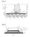
- Figs. 7A and 7B show an example of a light emitting module employing such the planar light emitting panel.
- the light emitting module 101 includes: a light emitting panel 103 having a light emitting unit 102; a circuit board 104 for supplying electric power to the light emitting unit 102 of the light emitting panel 103; and a case unit 105 in which the light emitting panel 103 and the circuit board 104 are housed.
- a plurality of feeding electrodes (103a, 103b) are arranged along a periphery of the light emitting panel 103.
- Each of the plurality of feeding electrodes (103a, 103b) is electrically connected to either a positive electrode or a negative electrode of the light emitting unit 102.
- the case unit 105 includes a case body 150 and a cover 151.
- the light emitting panel 103 is supported by the case body 150.
- the cover 151 is arranged at a non-emitting side (at a reverse side to a side on which the light emitting panel 103 is arranged) of the case body 150.
- the cover 151 is adapted to protect the circuit board 104 and the like.
- Some of feeding electrodes from among the plurality of feeding electrodes (103a, 103b) are electrically connected to the circuit board 104 by wirings 107.
- the feeding electrodes having same polarity are connected one another by wirings 108.
- a wire bonding method is adopted by which a wire formed of such as aluminum is used for the wiring.
- the wiring ( 107, 108 ) is provided in an arch-shape to have some slack as shown in Fig. 8A in order to avoid a breaking of the wire caused of such as thermal expansion and contraction of the wire.
- the plurality of feeding electrodes are needed to be arranged at the periphery of the light emitting panel 103 as shown in Fig. 7A, 7B .
- the module is required to have sufficient space for accommodating the wire (each of the wires is provided in an arch-shape). Therefore, as shown in Fig.
- the cover 151 of the module is required to be designed to have a predetermined thickness (sufficient "height") at the periphery thereof.
- a user is likely to feel that the module is comparatively thick (user is likely to receive a thickness impression).
- periphery of the cover 151 may be chamfered.
- the wiring 108 possibly comes into contact with the inner surface of the cover 151 to be damaged.
- the present invention is developed in view of above problem, and it is an object of the present invention to provide a light emitting module having a streamlined shape which gives a reduced thickness impression of the case unit for housing the light emitting panel (i.e. which has reduced thickness of the light emitting module at the periphery).
- a light emitting module of the present invention comprising: a light emitting panel which has a light emitting unit and a plurality of feeding electrodes, said light emitting unit comprising a positive electrode, a negative electrode and a light emitting layer provided therebetween, each of said plurality of feeding electrodes being electrically connected to either said positive electrode or said negative electrode; a circuit board which is electrically connected to said plurality of feeding electrodes and is configured to supply electric power to said light emitting unit; and a case unit in which said light emitting panel and said circuit board are housed, wherein said plurality of feeding electrodes are arranged at a peripheral region of said light emitting panel, wherein said circuit board is situated nearer the center in relation to the peripheral region of said light emitting panel, and wherein the electrical connection between said feeding electrode and said circuit board is obtained by a wiring which is elongated in the direction from a center region to a peripheral region of said light emitting panel.
- said plurality of feeding electrodes are arranged in such a manner that the feeding electrodes having same polarity are not arranged adjacent one another.
- circuit components are mounted on said circuit board, said circuit components being arranged so as to be gathered at a center region of said light emitting panel.
- said light emitting module further comprises a land-board for wiring connection, said land-board being situated nearer the center in relation to said plurality of feeding electrodes, and wherein the electrical connection between said feeding electrode and said circuit board is obtained through said land-board.
- said circuit board and said land-board are provided separately from each other.
- said plurality of feeding electrodes are arranged along a side of said light emitting panel, and wherein said plurality of feeding electrodes and said circuit board are electrically connected by a plurality of said wirings, each and every of said plurality of wirings being elongated along a direction orthogonal to the arrangement direction of said plurality of feeding electrodes.
- said case unit comprises a case body to which said light emitting panel and said circuit board are attached, said case body being formed with a plurality of openings at positions corresponding to said plurality of feeding electrodes of said light emitting panel, wherein said circuit board is arranged on said case body of a reverse side to a side to which said light emitting panel is attached, said circuit board being situated nearer the center in relation to said plurality of openings, and wherein each of wirings which are connected to the feeding electrodes is arranged so as to pass through such one of said plurality of openings that is formed for the concerned feeding electrode.
- said light emitting module further comprises a land-board for wiring connection, said land-board being arranged on said case body of a side to which said circuit board is attached, said land-board being situated nearer the center in relation to said plurality of openings, wherein each of said plurality of feeding electrodes is electrically connected to said land-board by a wiring, said wiring being elongated along a direction orthogonal to the arrangement direction of said plurality of feeding electrodes, said wiring being arranged so as to pass through such one of said plurality of openings that is formed for the concerned feeding electrode, and wherein said land-board is electrically connected to said circuit board by a wiring which is elongated along a direction orthogonal to the arrangement direction of said plurality of feeding electrodes.
- said light emitting unit is an electroluminescence device which comprises a planar positive electrode, a planar negative electrode and a light emitting layer provided therebetween.
- the electrical connection between the feeding electrode and the circuit board is obtained by a wiring which is elongated from a center region to a peripheral region of the light emitting panel. Therefore, the top portion of the wiring is located nearer the center in relation to the peripheral region of the light emitting panel. With this configuration, the wiring becomes less possible to be contacted with the inner surface of the cover even when using the cover having a chamfered periphery. Therefore, the present invention can suppress the thickness impression of the light emitting module, and can provide the light emitting module of a streamlined shape.
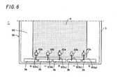
- a light emitting module 1 of the present embodiment includes: a light emitting panel 3 having a light emitting unit 2; a circuit board 4 for supplying electric power to the light emitting unit 2; and a case unit 5 in which the light emitting panel 3 and the circuit board 4 are housed.
- the light emitting unit 2 is composed of a positive electrode 2a, a negative electrode 2c and a light emitting layer 2b provided therebetween (as described in detail later).
- the light emitting unit is composed of an organic EL device.
- each of the positive electrode 2a, the light emitting layer 2b, and the negative electrode 2c is formed in a planar shape (a rectangular shape in a planar view).
- the light emitting panel 3 has a plurality of feeding electrodes (3a, 3b) each of which is electrically connected to either the positive electrode 2a or the negative electrode 2c of light emitting unit 2.
- the light emitting panel 3 has a plurality of first feeding electrodes 3a each of which is electrically connected to the positive electrode 2a and a plurality of second feeding electrodes 3b each of which is electrically connected to the negative electrode 2c.
- the plurality of feeding electrodes (3a, 3b) are arranged at a peripheral region of the light emitting panel 3, and are electrically connected to the circuit board 4.
- the plurality of feeding electrodes (3a, 3b) are arranged along a side (sides) of the light emitting panel 3.
- the circuit board 4 is arranged nearer the center in relation to the peripheral region of the light emitting panel 3.
- the light emitting module 1 is configured to emit light in the direction of dashed arrow shown in the figures.
- the direction of the dashed arrow is referred to as “emitting direction”
- the directly opposite direction of the dashed arrow is referred to as "non-emitting direction”.
- the light emitting module 1 includes a land-board for wiring connection (land-board) 6. Especially in the present embodiment, the light emitting module includes a pair of land-boards 6.
- the land-board 6 is arranged nearer the center in relation to the plurality of feeding electrodes (3a, 3b).
- Each of the feeding electrodes (3a, 3b) is electrically connected to the circuit board 4 via the land-board 6.
- the electrical connection between the circuit board 4 and the land-board 6 is obtained by a wiring 7.
- the electrical connections between the land-board 6 and the feeding electrodes (3a, 3b) are obtained by the wirings 8 (8a, 8b), respectively.
- the first feeding electrode 3a is defined as an electrode which is connected to the positive electrode 2a of the light emitting unit 2.
- the second feeding electrode 3b is defined as an electrode which is connected to the negative electrode 2c of the light emitting unit 2.
- Each of the wirings (7, 8) is elongated in the direction from a center region to a peripheral region of the light emitting panel 3.
- each of the wirings 8 is elongated in the direction orthogonal to the arrangement direction of the feeding electrodes (3a, 3b) to which the wiring 8 in question is connected.
- the wiring 7 also is elongated in the direction orthogonal to the arrangement direction of the feeding electrodes (3a, 3b).
- the case unit 5 includes: a case body 50 for supporting the light emitting panel 3; and a cover 51 for protecting the circuit board 4 and the like.
- the cover 51 is arranged at the non-emitting direction with respect to the case body 50.
- the shape of the light emitting panel 3 is determined properly depending on the intended use of the light emitting module 1.
- the case unit 5 is formed to have a shape according to the shape of the light emitting panel 3. In the present example, the light emitting panel 3 is formed in an elongated rectangular shape as shown in figures.
- the case unit 5 can be made of: plastics material such as ABS resin, acrylic resin, polystyrene resin or the like; or metal material such as aluminum plate with processing an insulation treatment on its surface.
- the case body 50 is formed in a tin-shape having a depression 52 which is opened in the emitting direction (refer to Fig. 4 ).
- the light emitting panel 3 is fit into the depression 52.
- the bottom of the depression 52 includes a supporting portion 53 for supporting the light emitting panel 3 and a plurality of openings 54 for exposing therethrough the plurality of feeding electrodes (3a, 3b) to the non-emitting directional side.
- the openings 54 are formed at the positions corresponding to the feeding electrodes (3a, 3b), respectively.
- the light emitting panel 3 is attached to the supporting portion 53 by an adhesion member (not shown in figures).
- the adhesion member is preferred to serve as a buffer, filler, and the like.
- the circuit board 4 and the land-board 6 are arranged on the non-emitting directional side surface of the supporting portion 53.
- the circuit board 4 is arranged on a middle region of the supporting portion 53.
- the circuit board 4 is arranged parallel with the longitudinal direction of the supporting portion 53.
- the pair of land-boards 6 are arranged at both ends of the circuit board 4 so as to place the circuit board 4 between the pair of land-boards 6.
- Each of the land-boards 6 is arranged orthogonal to the longitudinal direction of the supporting portion 53.
- Each of the circuit board 4 and the land-boards 6 is fixed to the supporting portion 53 by such as an acrylic double-stick tape in which a core material is contained that has a superior heat resistance property, a superior moisture resistance property and a superior stress relaxation property.
- the supporting portion 53 is provided with an engaging part 55 with which the cover 51 is engaged.
- the case body 50 has a peripheral wall 59 (refer to Fig. 4 ) formed at the outer periphery of the rectangular plate shaped supporting portion 53 so that the peripheral wall 59 surrounds the supporting portion 53.
- the depression 52 is composed by a space surrounded by the supporting portion 53 and the peripheral wall 59.
- the light emitting panel 3 is attached to the depression 52.
- the plurality of openings 54 are formed at the longitudinal both ends of the supporting portion 53 at the positions corresponding to the feeding electrodes (3a, 3b) of the light emitting panel 3.
- the openings 54 are formed side-by side along the side edge of the supporting portion 53.
- the circuit board 4 and the land-board 6 are arranged on the case body 50 of a reverse side to a side to which the light emitting panel 3 is attached (that is, arranged on the non-emitting directional side surface of the case body 50).
- the circuit board 4 and the land-boards 6 are arranged at positions of closer to the center than the positions of the plurality of openings 54 of the case body 50.
- the circuit board 4 is arranged at a position of closer to the center than the arrangement position of the land-board 6.
- the land-board 6 is arranged so that the longitudinal direction thereof extends along the arrangement direction of the plurality of openings 54.
- the cover 51 is formed in a tin-shape having a depression 56 which is opened in the emitting direction (refer to Fig. 4 ).
- This depression 56 gives a space for housing the circuit board 4, the land-board 6, and the wirings (7, 8) therein.
- the outer periphery of the cover 51 is chamfered so as to be inclined toward the edge of the cover 51.
- the cover 51 has a further depressed recess 57 formed at a center region thereof.
- the recess 57 gives a space for housing therein a variety of circuit components 41 mounted on the circuit board 4.
- the cover 51 is formed at the side face thereof with an engaging part 58 with which the engaging part 55 of the case body 50 is engaged.
- the cover 51 is formed to have a dimension such that all of the plurality of openings 54 formed at the supporting portion 53 are covered by the cover 51 when the engaging parts 58 formed at both side faces are engaged with the engaging parts 55 (refer to Fig. 5 ).
- the circuit board 4 is formed of a common printed wiring board which is provided with printed circuits (not shown in figures) and terminals (42a, 42b) adapted to be connected to the land-board 6 by the wirings 7 (refer to Fig. 2 ).
- the wiring board is preferred to be formed of a substrate having a flame resistance property and a low conductive property, such as a glass fiberboard (for example, FR-4 (FLAME Retardant Type 4)) made by impregnating a fiberglass cloth with epoxy resin and then hardened.
- the circuit board 4 is provided thereon with a various kinds of circuit components 41 such as a dimming control circuit configured to receive a dimming control signal from a dimming device or the like provided outside the light emitting module 1, a current control circuit configured to control the electric current supplied to the light emitting panel 3, and the like.
- Each of the terminals (42a, 42b) of the printed circuits is preferably plated with such as gold.
- the circuit board 4 is provided thereon with a connector (not shown in figures) configured to receive electric power from outside and to connect with another light emitting module 1.
- the cover 51 is formed with a terminal opening (not shown in figures) thorough which the connector is exposed.
- the land-board 6 is formed of a common printed wiring board as similar with the circuit board 4. As shown in Fig. 2 , the land-board 6 is provided with a positive electrode line 6a and a negative electrode line 6b each of which is formed parallel with the longitudinal direction of the land-board 6. That is, the land-board 6 is arranged such that each of the positive electrode line 6a and the negative electrode line 6b is elongated along the arrangement direction of the feeding electrodes (3a, 3b).
- the positive electrode line 6a is electrically connected to the positive-side terminal 42a of the circuit board 4 by a wiring 7a
- the negative electrode line 6b is electrically connected to the negative-side terminal 42b of the circuit board 4 by a wiring 7b.
- each of the wirings 7 (7a, 7b) is arranged so as to extend from the renter region of the light emitting panel 3 to the peripheral region of the light emitting panel 3.
- the positive electrode line 6a is electrically connected to the first feeding electrode 3a by the wiring 8a
- the negative electrode line 6b is electrically connected to the second feeding electrode 3b by the wiring 8b.
- each of the wirings 8 (8a, 8b), which connects between the feeding electrode (3a, 3b) and the positive electrode line 6a or the negative electrode line 6b of the land-board 6, is arranged so as to extend from the center region of the light emitting panel 3 to the peripheral region of the light emitting panel 3.
- each of the wirings 8 (8a, 8b) extends in the direction orthogonal to the arrangement direction of the feeding electrodes (3a, 3b) so as to pass through one of the plurality of openings 54 (refer to Fig. 1 B) .
- the positive electrode line 6a and the negative electrode line 6b may be coated with an insulation material with exposing only the terminals (not shown in figured).
- the configuration of the light emitting panel 3 is explained below with reference to Fig. 1A, Fig. 1 B and Fig. 3 .
- the light emitting panel 3 is composed of: a substrate 31 having a light transmissive property; the light emitting unit 2 formed on the substrate 31; and a sealing member which coats the outer side of the light emitting unit 2.
- the light emitting unit 2 is composed of: the positive electrode 2a formed of a transparent conductive film; the light emitting layer 2b having a light emission capability; and the negative electrode 2c having a light-reflective property, wherein which are stacked on the substrate 31 in this order.
- the substrate 31 is formed of a translucent glass such as a soda-lime glass or an alkali-free glass, or formed of a translucent resin material.
- the substrate 31 is formed in a rectangular plate shape.
- the substrate 31 may be provided therein with a phosphor which is excited by the light of the light emitting layer 2b and to emit light having longer wavelength than the light of the light emitting layer 2b.
- the positive electrode 2a is adapted to inject a hole in the light emitting layer 2b.
- the positive electrode 2a is made of an electrode material such as metal, alloy, conductive compound or mixture of them having a large work function, and preferably of the material having a work function of 4 [eV] or more. It is preferred that the electrode material of the positive electrode 2a is such a translucent conductive material of ITO (indium tin oxide), SnO 2 (tin oxide), ZnO (zinc oxide) or the like.
- the positive electrode 2a is formed on the surface of the substrate 31 by deposing and patterning these electrode materials through the vacuum evaporation method, the sputtering method, or the like.
- the light emitting layer 2b is formed by using such as anthracene, naphthalene, pyrene, tetracene, tris-(8-hydroxyquinolinate)-aluminum complex, tris-(4-methyl-8-quinolinate)-aluminum complex or distyrylarylene derivative; compound or polymer material which includes above luminescent element as a radical; various kinds of fluorochrome; or mixture of them.
- the light emitting panel 3 employs organic material for the light emitting layer 2b, but the present invention is not limited thereto. Inorganic material may be employed for the light emitting layer 2b.
- the light emitting layer 2b is formed on the surface of the positive electrode 2a by deposing and patterning the above described material through the vacuum evaporation method or the like.
- the light emitting layer 2b may include a plurality of layers formed of different materials, and also may further include a buffer layer or the like for adjusting the potential between these layers.
- the negative electrode 2c is adapted to inject an electron in the light emitting layer 2b.
- the negative electrode 2c is made of an electrode material of metal, alloy, conductive compound or mixture of them having a small work function, and preferably of the material having a work function of 5 [eV] or less. It is preferred that the electrode material of the negative electrode 2c is such a reflective conductive material of lithium, aluminum, aluminum-lithium alloy, mixture of magnesium and silver, mixture of Al and Al 2 O 3 , mixture of Al and LiF, or the like.
- the negative electrode 2c is formed by similar method with the positive electrode 2a.
- a hole injection/transport layer (not shown in figures) for facilitating the hole injecting effect from the positive electrode 2a to the light emitting layer 2b is preferably provided between the positive electrode 2a and the light emitting layer 2b.
- An electron injection/transport layer (not shown in figures) for facilitating the electron injecting effect from the negative electrode 2c to the light emitting layer 2b is preferably provided between the light emitting layer 2b and the negative electrode 2c.
- the light emitting panel 3 is formed into the above configuration, and the light emitting layer 2b emits light when a predetermined electric power is supplied from the circuit board 4.
- the light emitted from the light emitting layer 2b is (reflected by the negative electrode 2c and is) transmitted through the positive electrode 2a, and is extracted toward outward of the light emitting panel 3 from the substrate 31 side.
- the light emitting panel 3 is preferably provided on its emitting surface (on the surface of the light emitting panel 3 of the emitting directional side) with a protection layer made of acrylic resin or the like for protecting the substrate 31 from being damaged or stained, a diffusion layer for improving the light extracting efficiency from the substrate 31 side, and the like (not shown in figures).
- transparent electrode material such as ITO
- the present embodiment further includes an auxiliary electrode of a patterned metal which can suppress the voltage drop in the electrode made of such as ITO.
- the auxiliary electrode is formed so as to have an opening at a position where the light emitting layer 2b is formed, in order not to disturb the light emission toward the substrate 31 side.
- the auxiliary electrode is formed by the sputtering method or the like.
- the periphery of the opening of the auxiliary electrode is contacted with the positive electrode 2a (which is made of ITO etc.), and some parts of the auxiliary electrode are extended to form the pattern of the above described first feeding electrodes 3a which are served for an extracted positive electrode (refer to Fig. 1A , Fig. 2 ).
- the positive electrode 2a is formed in a rectangular shape in a plain view
- the auxiliary electrode is preferably formed in a rectangular frame shape surrounding the positive electrode 2a.
- the first feeding electrodes 3a may be formed of a plurality of rectangular conductive portions which are extended from two sides of the auxiliary electrode, which are the sides parallel with the width directional both sides of the light emitting panel 3, toward the longitudinal direction of the light emitting panel 3 (refer to Fig. 1A ). It is preferred that the auxiliary electrode and/or the first feeding electrodes 3a is provided thereon with an insulation film (not shown in figures) made of a material having small electric conductivity such as polyimide, epoxy resin or the like, in order to prevent a short circuit between the negative electrode 2c and the auxiliary electrode or the first feeding electrodes 3a.
- the first feeding electrode 3a (and the auxiliary electrode) is preferably made of metal which has a superior adhesion property with ITO, which has a superior electric conductivity, which is hardly deteriorated by humidity and heat, and which is capable of being bonded through the ultrasonic bonding method.
- metal which has a superior adhesion property with ITO, which has a superior electric conductivity, which is hardly deteriorated by humidity and heat, and which is capable of being bonded through the ultrasonic bonding method.
- it may be composed of: a three-layers sputtered film of a molybdenum layer, an aluminum layer and a molybdenum layer; an alloy film of silver-palladium-copper; or the like.
- the second feeding electrodes 3b which are served for an extracted negative electrode, are formed on the substrate 31 in a pattern so as to be contacted with the negative electrode 2c as well as not to be contacted with the positive electrode 2a and the first feeding electrodes 3a.
- the second feeding electrode 3b can be made of the metal which is recited with regard to the first feeding electrode 3a.
- the second feeding electrode 3b can be made of the same material with the first feeding electrode 3a.
- it may be formed as a part of the auxiliary electrode of the negative electrode 2c.
- These feeding electrodes (3a, 3b) can be formed simultaneously in a same process. After the patterning of them, the light emitting unit 2 (which has the light emitting layer 2b etc.) is formed.
- the negative electrode 2c of the light emitting unit 2 is electrically connected to the second feeding electrode 3b when forming the negative electrode 2c.
- Each of these electrodes and the light emitting unit 2 is formed in a thin film having a nanometer size, and can be regarded to have substantially almost no thickness compared with the substrate 31.
- the plurality of feeding electrodes (3a, 3b) are arranged in such a manner that the feeding electrodes (3a, 3b) having same polarity are not arranged adjacent one another. That is, the feeding electrodes (3a, 3b) of a same polarity are arranged in distant positions with one another. Therefore, the power feeding points are dispersed in positions, it enables to equalize the applying voltage in plain to the light emitting unit 2. As a result, the dispersion of brightness can be reduced.
- the sealing member 32 is bonded to be fixed to the substrate 31 so as to cover the light emitting unit 2 and the like with exposing the feeding electrodes (3a, 3b).
- the sealing member 32 is formed of a copper foil without pinhole, which has a superior sealing property.
- the sealing member 32 is fixed to the substrate 31 via a non-conductive adhesive such as epoxy resin, silicone resin, or the like. Thereby, an insulation section (not shown in figures) made of the non-conductive adhesive is formed between the sealing member 32 and the light emitting unit 2, and therefore the sealing member 32 is made to be contactless with the light emitting unit 2. This configuration makes it possible to prevent a short circuit between the sealing member 32 and the light emitting unit 2.
- the circuit board 4 and the land-board 6 is connected by bonding the wirings 7, and the land-board 6 and the feeding electrodes (3a, 3b) are connected by bonding the wirings 8.
- Each of the wirings (7, 8) is preferably formed of a pure aluminum wire.
- the pure aluminum wire can be connected to each of the terminals in a short time under an ordinary temperature by way of the ultrasonic bonding method. Size (diameter) of each of the wirings (7, 8) is determined according to the material, consumption current and the like of the light emitting panel 3.
- each of the wirings 8, which connects between the feeding electrode (3a, 3b) and the land-board 6, is arranged so as to be elongated in the direction from the center region of the light emitting panel 3 to the peripheral region of the light emitting panel 3. Therefore, the top portion of the wiring 8 is located nearer the center in relation to the peripheral region of the light emitting panel 3.
- the wiring 8 becomes less possible to be contacted with the inner surface of the cover 51 even when using the cover 51 having a chamfered periphery. Therefore, the present embodiment can employ such the cover 51 having chambered periphery as shown in Fig. 5 , can suppress the thickness impression of the light emitting module 1, and can provide the light emitting module 1 of a streamlined shape.
- the circuit components 41 mounted on the circuit board 4 are arranged so as to be gathered at a center region of the light emitting panel 3.
- the center region of the light emitting module 1 may becomes thick, the other region thereof can be made thin as shown in Fig. 5 . Therefore, the module itself can be formed in a streamlined shape.
- electric wirings for connecting between a plurality of the light emitting modules 1 can be arranged at the outward space of the "thinned-region" of the light emitting module 1. Therefore, this configuration enables to increase the degree of freedom in the design of illumination apparatus to which the light emitting module 1 is attached.
- the land-board 6 is arranged nearer the center in relation to the feeding electrodes (3a, 3b) (that is, in relation to the openings 54).
- the feeding electrodes (3a, 3b) are electrically connected to the circuit board 4 via the land-board 6 (refer to Fig. 2 ). Therefore, the length of the wiring 8 can be shortened by locating the land-board 6 near the feeding electrodes (3a, 3b). With this configuration, expansion/contraction amount of the wiring 8 caused by the heat of the circuit board 4 etc. can be minimized, and therefore the thermal stress applied on the connection point and the wiring 8 can be minimized. Therefore, this configuration enables to suppress the occurrence of the breaking of the wiring 8.
- the circuit board 4 and the land-board 6 are arranged separately, and they are connected by the wiring 7.
- the wiring 8, which connects between the land-board 6 and the feeding electrodes (3a, 3b), is hardly affected by the thermal expansion/contraction of the circuit board 4. Therefore, this configuration enables to suppress the occurrence of the breaking of the wiring 8.
- the light emitting panel 3 is attached to the supporting portion 53 on the front side surface (on the surface of the emitting directional side), and the circuit board 4 is attached to the supporting portion 53 on the back side surface (on the surface of the non-emitting directional side) in the case body 50.
- This configuration enables to reliably insulate between the light emitting unit 2 of the light emitting panel 3 and the circuit board 4. Further, this configuration enables to make the light emitting module 1 in a compact size.
- the supporting portion 53 of the case body 50 is formed with the openings 54 at positions each of which corresponds to the position of the feeding electrode (3a, 3b) of the light emitting panel 3.
- the wiring 8 is extended from the feeding electrode (3a, 3b) so as to pass through one of the openings 54 which is formed for the concerned feeding electrode (3a, 3b). This configuration enables to prevent from occurring a short circuit between the first feeding electrode 3a and the second feeding electrode 3b.
- a patterned circuit (not shown in figures) is formed on the circuit board 4.
- the patterned circuit is arranged in parallel with the feeding electrodes (3a, 3b).
- the feeding electrode (3a, 3b) is electrically connected directly to the circuit board 4 by a wiring 9.
- the circuit board 4 is provided with terminals (43a, 43b) for connecting the wirings 9. That is, the first feeding electrode 3a is electrically connected to the positive side terminal 43a of the circuit board 4 by a wiring 9a, and the second feeding electrode 3b is electrically connected to the negative side terminal 43b of the circuit board 4 by a wiring 9b.
- each of the wirings 9 (9a, 9b) is elongated in the direction from the center region to the peripheral region of the light emitting panel 3, as similar with the above described (refer to Fig. 2 ) wirings 8.
- Each of the wirings 9 (9a, 9b) is extended from the feeding electrode (3a, 3b) so as to pass through one of the openings 54 which is formed for the feeding electrode (3a, 3b) in question.
- Other configurations are similar with those of above described embodiment.
- this configuration enables to simplify the working process and to improve the productivity of the module.
- the present invention is not limited to the above described embodiment and can be applied with a various of modification, so long that the feeding electrodes are arranged along the periphery of the light emitting panel and that the feeding electrode is connected to the circuit board by the wiring which is elongated from the center region to the peripheral region of the light emitting panel.
- the feeding electrodes (3a, 3b) are formed at the longitudinal both ends of the light emitting panel 3 in the above described embodiment, the feeding electrodes also can be formed at both ends of a direction orthogonal to the embodiment (that is, formed at the width directional both ends of the light emitting panel 3; not shown in figures).
- a plurality of feeding electrodes can be arranged along the longitudinal direction of the light emitting panel 3.
- a land-board can be provided near these feeding electrodes.
Landscapes
- Engineering & Computer Science (AREA)
- Manufacturing & Machinery (AREA)
- Physics & Mathematics (AREA)
- Optics & Photonics (AREA)
- Electroluminescent Light Sources (AREA)
- Planar Illumination Modules (AREA)
- Arrangement Of Elements, Cooling, Sealing, Or The Like Of Lighting Devices (AREA)
Applications Claiming Priority (2)
| Application Number | Priority Date | Filing Date | Title |
|---|---|---|---|
| JP2010239103A JP5830711B2 (ja) | 2010-10-25 | 2010-10-25 | 発光モジュール |
| PCT/JP2011/072328 WO2012056848A1 (ja) | 2010-10-25 | 2011-09-29 | 発光モジュール |
Publications (2)
| Publication Number | Publication Date |
|---|---|
| EP2634474A1 true EP2634474A1 (de) | 2013-09-04 |
| EP2634474A4 EP2634474A4 (de) | 2018-01-17 |
Family
ID=45993578
Family Applications (1)
| Application Number | Title | Priority Date | Filing Date |
|---|---|---|---|
| EP11835988.4A Withdrawn EP2634474A4 (de) | 2010-10-25 | 2011-09-29 | Lichtemittierendes modul |
Country Status (5)
| Country | Link |
|---|---|
| US (1) | US9013096B2 (de) |
| EP (1) | EP2634474A4 (de) |
| JP (1) | JP5830711B2 (de) |
| CN (1) | CN103189679B (de) |
| WO (1) | WO2012056848A1 (de) |
Cited By (1)
| Publication number | Priority date | Publication date | Assignee | Title |
|---|---|---|---|---|
| WO2015144925A1 (en) | 2014-03-27 | 2015-10-01 | Koninklijke Philips N.V. | Luminaire |
Families Citing this family (5)
| Publication number | Priority date | Publication date | Assignee | Title |
|---|---|---|---|---|
| JP5789757B2 (ja) * | 2011-03-04 | 2015-10-07 | パナソニックIpマネジメント株式会社 | 照明装置 |
| JP6078295B2 (ja) * | 2012-10-29 | 2017-02-08 | 株式会社カネカ | 有機el装置 |
| JP2015079737A (ja) * | 2013-09-11 | 2015-04-23 | パナソニックIpマネジメント株式会社 | 発光モジュール |
| CH709411B1 (de) * | 2014-03-26 | 2018-03-29 | Ribag Licht Ag | Leuchtelement mit OLED. |
| JP2019053994A (ja) * | 2018-11-14 | 2019-04-04 | パイオニア株式会社 | 発光装置及び発光システム |
Family Cites Families (13)
| Publication number | Priority date | Publication date | Assignee | Title |
|---|---|---|---|---|
| JP2003051385A (ja) * | 2001-08-06 | 2003-02-21 | Sony Corp | 表示装置の製造方法 |
| KR100702517B1 (ko) * | 2005-05-17 | 2007-04-04 | 엘지전자 주식회사 | 유기 전계 발광 소자 |
| EP1933194B1 (de) * | 2006-12-13 | 2014-01-08 | LG Display Co., Ltd. | Rückbeleuchtungseinheit und Flüssigkristallanzeigemodul damit |
| JP5289709B2 (ja) | 2007-01-09 | 2013-09-11 | 株式会社ジャパンディスプレイ | 調光機能を備えた画像表示装置 |
| DE102008013031B4 (de) * | 2008-03-07 | 2019-07-25 | Osram Oled Gmbh | Optoelektronisches Bauelement |
| US8120257B2 (en) | 2008-06-06 | 2012-02-21 | Rohm Co., Ltd. | Organic electroluminescence lighting device |
| JP2009295487A (ja) * | 2008-06-06 | 2009-12-17 | Rohm Co Ltd | 有機el照明装置 |
| JP2010003600A (ja) * | 2008-06-23 | 2010-01-07 | Panasonic Electric Works Co Ltd | 面状型照明器具 |
| JP5541872B2 (ja) * | 2009-02-26 | 2014-07-09 | パナソニック株式会社 | 面状発光装置および照明器具 |
| JP5394106B2 (ja) | 2009-03-26 | 2014-01-22 | パナソニック株式会社 | 面状発光素子に対する給電方法 |
| JP5796171B2 (ja) * | 2009-10-27 | 2015-10-21 | パナソニックIpマネジメント株式会社 | 発光モジュール |
| JP5559586B2 (ja) * | 2010-04-07 | 2014-07-23 | パナソニック株式会社 | 有機elモジュール |
| JP5807177B2 (ja) * | 2010-05-26 | 2015-11-10 | パナソニックIpマネジメント株式会社 | 発光モジュール |
-
2010
- 2010-10-25 JP JP2010239103A patent/JP5830711B2/ja not_active Expired - Fee Related
-
2011
- 2011-09-29 EP EP11835988.4A patent/EP2634474A4/de not_active Withdrawn
- 2011-09-29 US US13/816,752 patent/US9013096B2/en not_active Expired - Fee Related
- 2011-09-29 CN CN201180051707.XA patent/CN103189679B/zh not_active Expired - Fee Related
- 2011-09-29 WO PCT/JP2011/072328 patent/WO2012056848A1/ja not_active Ceased
Non-Patent Citations (1)
| Title |
|---|
| See references of WO2012056848A1 * |
Cited By (2)
| Publication number | Priority date | Publication date | Assignee | Title |
|---|---|---|---|---|
| WO2015144925A1 (en) | 2014-03-27 | 2015-10-01 | Koninklijke Philips N.V. | Luminaire |
| US10731808B2 (en) | 2014-03-27 | 2020-08-04 | Signify Holding B.V. | Luminaire with multiple light emissive surfaces |
Also Published As
| Publication number | Publication date |
|---|---|
| US20130134866A1 (en) | 2013-05-30 |
| JP5830711B2 (ja) | 2015-12-09 |
| CN103189679B (zh) | 2015-06-03 |
| US9013096B2 (en) | 2015-04-21 |
| EP2634474A4 (de) | 2018-01-17 |
| CN103189679A (zh) | 2013-07-03 |
| JP2012094303A (ja) | 2012-05-17 |
| WO2012056848A1 (ja) | 2012-05-03 |
Similar Documents
| Publication | Publication Date | Title |
|---|---|---|
| CN101341608B (zh) | 有机led器件 | |
| CN102054935B (zh) | 有机发光二极管照明装置 | |
| KR101084246B1 (ko) | 유기 발광 조명 장치 | |
| US8686635B2 (en) | Organic light emitting diode lighting apparatus | |
| WO2010098392A1 (ja) | 面状発光装置 | |
| US9013096B2 (en) | Light emitting module | |
| US8764209B2 (en) | Light module | |
| JP5702736B2 (ja) | エレクトロルミネセント素子 | |
| KR101513443B1 (ko) | 인쇄 회로 기판 상의 광원 디바이스 그리고 복수 개의 광원 디바이스들을 포함하는 광원 어레인지먼트 | |
| JP2005338419A (ja) | 面発光装置用封止体及び面発光装置 | |
| TW201407847A (zh) | 有機發光二極體模組 | |
| JP4679922B2 (ja) | El光源体 | |
| WO2016132870A1 (ja) | 有機elパネル | |
| JP2000357585A (ja) | 有機el素子 | |
| CN108119783B (zh) | Oled发光模块 | |
| JP2011249144A (ja) | 発光モジュール | |
| US7011987B2 (en) | Method of fabricating organic electroluminescence panel package | |
| CN103733370A (zh) | 有机发光元件及包括其的发光装置 | |
| CN208572516U (zh) | 显示装置 | |
| US20140111084A1 (en) | Oled lighting device | |
| JP2003007474A (ja) | 有機電界発光素子 | |
| KR20140035802A (ko) | Oled 조명 모듈 | |
| CN103974484A (zh) | 照明器具 | |
| TW201526324A (zh) | 發光二極體結構 |
Legal Events
| Date | Code | Title | Description |
|---|---|---|---|
| PUAI | Public reference made under article 153(3) epc to a published international application that has entered the european phase |
Free format text: ORIGINAL CODE: 0009012 |
|
| 17P | Request for examination filed |
Effective date: 20130219 |
|
| AK | Designated contracting states |
Kind code of ref document: A1 Designated state(s): AL AT BE BG CH CY CZ DE DK EE ES FI FR GB GR HR HU IE IS IT LI LT LU LV MC MK MT NL NO PL PT RO RS SE SI SK SM TR |
|
| DAX | Request for extension of the european patent (deleted) | ||
| RAP1 | Party data changed (applicant data changed or rights of an application transferred) |
Owner name: PANASONIC INTELLECTUAL PROPERTY MANAGEMENT CO., LT |
|
| RA4 | Supplementary search report drawn up and despatched (corrected) |
Effective date: 20171215 |
|
| RIC1 | Information provided on ipc code assigned before grant |
Ipc: H05B 33/06 20060101ALI20171212BHEP Ipc: H01L 51/52 20060101AFI20171212BHEP Ipc: F21V 23/00 20150101ALI20171212BHEP Ipc: F21Y 105/00 20160101ALI20171212BHEP Ipc: F21S 2/00 20160101ALI20171212BHEP |
|
| STAA | Information on the status of an ep patent application or granted ep patent |
Free format text: STATUS: THE APPLICATION IS DEEMED TO BE WITHDRAWN |
|
| 18D | Application deemed to be withdrawn |
Effective date: 20180719 |