EP2637302B1 - Mikrowellen-Halbleiterverstärker - Google Patents
Mikrowellen-Halbleiterverstärker Download PDFInfo
- Publication number
- EP2637302B1 EP2637302B1 EP12199817.3A EP12199817A EP2637302B1 EP 2637302 B1 EP2637302 B1 EP 2637302B1 EP 12199817 A EP12199817 A EP 12199817A EP 2637302 B1 EP2637302 B1 EP 2637302B1
- Authority
- EP
- European Patent Office
- Prior art keywords
- impedance
- transmission line
- electrical length
- reference plane
- characteristic impedance
- Prior art date
- Legal status (The legal status is an assumption and is not a legal conclusion. Google has not performed a legal analysis and makes no representation as to the accuracy of the status listed.)
- Active
Links
Images







Classifications
-
- H—ELECTRICITY
- H03—ELECTRONIC CIRCUITRY
- H03F—AMPLIFIERS
- H03F3/00—Amplifiers with only discharge tubes or only semiconductor devices as amplifying elements
- H03F3/04—Amplifiers with only discharge tubes or only semiconductor devices as amplifying elements with semiconductor devices only
-
- H—ELECTRICITY
- H03—ELECTRONIC CIRCUITRY
- H03F—AMPLIFIERS
- H03F1/00—Details of amplifiers with only discharge tubes, only semiconductor devices or only unspecified devices as amplifying elements
- H03F1/56—Modifications of input or output impedances, not otherwise provided for
- H03F1/565—Modifications of input or output impedances, not otherwise provided for using inductive elements
-
- H—ELECTRICITY
- H03—ELECTRONIC CIRCUITRY
- H03F—AMPLIFIERS
- H03F3/00—Amplifiers with only discharge tubes or only semiconductor devices as amplifying elements
- H03F3/60—Amplifiers in which coupling networks have distributed constants, e.g. with waveguide resonators
-
- H—ELECTRICITY
- H10—SEMICONDUCTOR DEVICES; ELECTRIC SOLID-STATE DEVICES NOT OTHERWISE PROVIDED FOR
- H10W—GENERIC PACKAGES, INTERCONNECTIONS, CONNECTORS OR OTHER CONSTRUCTIONAL DETAILS OF DEVICES COVERED BY CLASS H10
- H10W44/00—Electrical arrangements for controlling or matching impedance
-
- H—ELECTRICITY
- H10—SEMICONDUCTOR DEVICES; ELECTRIC SOLID-STATE DEVICES NOT OTHERWISE PROVIDED FOR
- H10W—GENERIC PACKAGES, INTERCONNECTIONS, CONNECTORS OR OTHER CONSTRUCTIONAL DETAILS OF DEVICES COVERED BY CLASS H10
- H10W44/00—Electrical arrangements for controlling or matching impedance
- H10W44/20—Electrical arrangements for controlling or matching impedance at high-frequency [HF] or radio frequency [RF]
-
- H—ELECTRICITY
- H03—ELECTRONIC CIRCUITRY
- H03F—AMPLIFIERS
- H03F2200/00—Indexing scheme relating to amplifiers
- H03F2200/222—A circuit being added at the input of an amplifier to adapt the input impedance of the amplifier
-
- H—ELECTRICITY
- H03—ELECTRONIC CIRCUITRY
- H03F—AMPLIFIERS
- H03F2200/00—Indexing scheme relating to amplifiers
- H03F2200/387—A circuit being added at the output of an amplifier to adapt the output impedance of the amplifier
-
- H—ELECTRICITY
- H03—ELECTRONIC CIRCUITRY
- H03F—AMPLIFIERS
- H03F2200/00—Indexing scheme relating to amplifiers
- H03F2200/423—Amplifier output adaptation especially for transmission line coupling purposes, e.g. impedance adaptation
-
- H—ELECTRICITY
- H10—SEMICONDUCTOR DEVICES; ELECTRIC SOLID-STATE DEVICES NOT OTHERWISE PROVIDED FOR
- H10W—GENERIC PACKAGES, INTERCONNECTIONS, CONNECTORS OR OTHER CONSTRUCTIONAL DETAILS OF DEVICES COVERED BY CLASS H10
- H10W44/00—Electrical arrangements for controlling or matching impedance
- H10W44/20—Electrical arrangements for controlling or matching impedance at high-frequency [HF] or radio frequency [RF]
- H10W44/226—Electrical arrangements for controlling or matching impedance at high-frequency [HF] or radio frequency [RF] for HF amplifiers
- H10W44/234—Arrangements for impedance matching
-
- H—ELECTRICITY
- H10—SEMICONDUCTOR DEVICES; ELECTRIC SOLID-STATE DEVICES NOT OTHERWISE PROVIDED FOR
- H10W—GENERIC PACKAGES, INTERCONNECTIONS, CONNECTORS OR OTHER CONSTRUCTIONAL DETAILS OF DEVICES COVERED BY CLASS H10
- H10W72/00—Interconnections or connectors in packages
- H10W72/50—Bond wires
- H10W72/541—Dispositions of bond wires
- H10W72/5445—Dispositions of bond wires being orthogonal to a side surface of the chip, e.g. parallel arrangements
-
- H—ELECTRICITY
- H10—SEMICONDUCTOR DEVICES; ELECTRIC SOLID-STATE DEVICES NOT OTHERWISE PROVIDED FOR
- H10W—GENERIC PACKAGES, INTERCONNECTIONS, CONNECTORS OR OTHER CONSTRUCTIONAL DETAILS OF DEVICES COVERED BY CLASS H10
- H10W90/00—Package configurations
- H10W90/701—Package configurations characterised by the relative positions of pads or connectors relative to package parts
- H10W90/751—Package configurations characterised by the relative positions of pads or connectors relative to package parts of bond wires
- H10W90/753—Package configurations characterised by the relative positions of pads or connectors relative to package parts of bond wires between laterally-adjacent chips
Definitions
- Embodiments described herein relate generally to a microwave semiconductor amplifier.
- the power added efficiency can be increased when the harmonic impedance seen from the output electrode of the semiconductor amplifying element toward the load is made close to the open-circuit impedance.
- the output impedance of a semiconductor amplifying element such as HEMT (high electron mobility transistor) and FET (field effect transistor) is capacitive at the fundamental. Efficiently extracting the signal amplified by the semiconductor amplifying element needs impedance matching between the output impedance of the semiconductor amplifying element and the external load at the fundamental.
- the impedance seen from the semiconductor amplifying element toward the load at the fundamental needs to be a desired inductive impedance.
- the impedance seen from the semiconductor element toward the load at the second harmonic needs to be near the open-circuit impedance.
- the impedance seen from the semiconductor amplifying element toward the load at the second harmonic can be set near the open-circuit impedance by providing a higher harmonic processing circuit using a stub near the chip.
- a matching circuit is cascaded via the higher harmonic processing circuit. This increases insertion loss and narrows the bandwidth.
- WO 00/75990 relates to a high frequency LDMOS power transistor device with relatively high input and output impedances.
- EP 1351300 describes a FET formed on a semiconductor substrate.
- a microwave semiconductor amplifier is provided as recited in claim 1.
- FIG. 1 is a schematic view showing the configuration of a microwave semiconductor amplifier according to a first embodiment.
- the microwave semiconductor amplifier includes an input terminal 10, an input matching circuit 12, a semiconductor amplifying element 14, an output matching circuit 20, and an output terminal 18.
- the microwave semiconductor amplifier is housed in a package.
- the DC circuit for supplying voltage to the semiconductor amplifying element 14 is not shown.
- the external load is Z L (n).
- Z L can be set to e.g. 50 ⁇ .
- the input matching circuit 12 is a matching circuit for the input impedance of the semiconductor amplifying element 14.
- the semiconductor amplifying element 14 can be e.g. a GaAs FET, GaAs HEMT (high electron mobility transistor), or GaN HEMT.
- a GaN HEMT based on a wide bandgap material can increase the breakdown voltage and obtain high output in the wavelength range from microwaves to millimeter waves.
- the output matching circuit 20 matches the output impedance of the semiconductor amplifying element 14 at the fundamental while maintaining high impedance for harmonics.
- the first embodiment includes an output matching circuit 20 for increasing impedance for the second harmonic among the harmonics.
- the output impedance Z out of the semiconductor amplifying element 14 can be determined by e.g. measuring the impedance during operation.
- the external load Z L is connected to the output terminal 18 of the output matching circuit 20.
- the output matching circuit 20 includes a bonding wire 15 and a first impedance converting circuit 16.
- the first impedance converting circuit 16 made of a first transmission line can be e.g. a microstrip line with characteristic impedance Z C1 and electrical length L1.
- the electrical length L can be determined by the following equation.
- a first reference plane P1 is defined as the position bonded by a wire from the output electrode of the semiconductor amplifying element 14.
- the effective length M of the transmission line is slightly shorter than the physical length of the first impedance converting circuit 16.
- L 360 ° ⁇ M / ⁇ eff
- the output electrode of the semiconductor amplifying element 14 is connected to the first impedance converting circuit 16 by the bonding wire 15.
- the first reference plane P1 for seeing the impedance toward the load is defined as the bonding position on the line pattern of the first impedance converting circuit 16.
- the second reference plane P2 for seeing the impedance toward the load is defined as the bonding position on the output electrode of the semiconductor amplifying element 14.
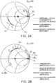
- FIG. 2A is an impedance diagram seen from the first reference plane toward the load.
- FIG. 2B is an impedance diagram seen from the second reference plane toward the load.
- the load impedance is denoted by z L
- the characteristic impedance of the first impedance converting circuit 16 is denoted by z C1 .
- the fundamental impedance and the second harmonic impedance seen toward the load draw a clockwise impedance locus along the dotted line as the distance from the load increases.
- the fundamental impedance z P1 is capacitive.
- the second harmonic impedance z P12 is inductive within a frequency range of double a lower limit frequency of the frequency band to double an upper limit frequency of the frequency band.
- the inductance of the bonding wire 15 is added.
- the fundamental impedance z P2 seen toward the load at frequency f is the sum of the fundamental impedance z P1 at the first reference plane P1 and a reactance of 2 ⁇ f ⁇ Lw/Z CC resulting from the inductance Lw of the bonding wire 15.
- the fundamental impedance z P2 is matched to the output impedance z out of the semiconductor amplifying element 14.
- z out depends on the semiconductor amplifying element 14.
- the fundamental impedance z P2 is made close to the output impedance z out * .
- the second harmonic impedance z P22 is the sum of the second harmonic impedance z P12 kept inductive at the first reference plane P1 and a reactance of 4 ⁇ f ⁇ Lw/Z CC .
- the second harmonic impedance z P22 is made closer to the open-circuit impedance (infinite impedance).
- the effect of suppressing the second harmonic depends on the first electrical length L1 of the first transmission line.
- the first electrical length L1 is larger than 0 degrees and 90 degrees or less at the upper limit frequency f H of the frequency band, because the circuit can then be downsized.
- the first electrical length L1 is generally 90 degrees at the upper limit frequency f H .
- the second harmonic impedance seen toward the load can be made close to the open-circuit impedance also by providing a stub circuit near the semiconductor amplifying element 14.
- this increases insertion loss.
- the fundamental impedance is made lower than at the chip end surface of the semiconductor amplifying element. This may make it difficult to match the fundamental impedance over a wide bandwidth.
- the first embodiment allows wide-band matching while suppressing the increase of insertion loss.
- the portion of the second harmonic impedance on the upper limit frequency side exceeds the inductive reactance region into the capacitive reactance region, the portion of the second harmonic impedance on the upper limit frequency side at the second reference plane P2, including the reactance resulting from the inductance Lw of the bonding wire 15, moves away from the infinite impedance toward the low impedance side. This decreases the effect of suppressing the second harmonic, and is undesirable.
- FIG. 3 is a graph describing the power added efficiency of the microwave semiconductor amplifier according to the first embodiment.
- the center frequency of the frequency band is e.g. in the range of 1-20 GHz.
- the output matching circuit 20 is matched with the fundamental and has a high impedance close to the open-circuit impedance for the second harmonic. Then, high power added efficiency can be achieved in the available frequency band between the lower limit frequency f L and the upper limit frequency f H of the frequency band. Furthermore, for instance, the lower limit frequency f L can be set to 0.9f C , and the upper limit frequency f H can be set to 1,1f C .
- the second harmonic component may fail to be reflected to the semiconductor amplifying element and leak to the external load. Then, the second harmonic component increases, and the power added efficiency decreases as shown by the dashed line.
- FIG. 4 is a schematic view showing the configuration of a microwave semiconductor amplifying circuit according to a second embodiment.
- the output matching circuit 20 of the second embodiment includes a bonding wire 15, a first impedance converting circuit 16, and a second impedance converting circuit 21 made of a second transmission line.
- the second impedance converting circuit 21 has a characteristic impedance Z C2 (Z C1 ⁇ Z C2 ⁇ Z L ) and an electrical length L2 of larger than 0 degrees and 90 degrees or less.
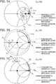
- FIG. 5A is an impedance diagram seen from the third reference plane toward the load.
- FIG. 5B is an impedance diagram seen from the first reference plane.
- FIG. 5C is an impedance diagram seen from the second reference plane.
- the characteristic impedance Z C2 of the second impedance converting circuit 21 can be made higher than the characteristic impedance of the first impedance converting circuit 16 in the first embodiment.
- the characteristic impedance Z C1 (Z C1 ⁇ Z C2 ⁇ Z L ) of the first impedance converting circuit 16 can be set lower than the characteristic impedance of the first impedance converting circuit 16 in the first embodiment.
- the second harmonic impedance z P12 is maintained to be inductive.
- the fundamental impedance z P2 seen from the second reference plane P2 toward the load, with the inductance of the bonding wire 15 added thereto, has a narrower variation range of the impedance locus in the frequency band f L -f H .
- the frequency characteristics of gain can be made flatter.
- the second harmonic impedance z P12 seen from the first reference plane P1 toward the load is maintained to be inductive.
- the second harmonic impedance z P22 is made closer to the open-circuit impedance because the inductance of the bonding wire 15 is added thereto. Accordingly, the power added efficiency can be made higher.
- the effect of suppressing the second harmonic depends on the electrical length L1 of the first transmission line and the electrical length L2 of the second transmission line.
- TABLE 1 shows an example of the dependence.
- TABLE 1 shows the second electrical length L2 at the lower limit frequency f L , the reflection coefficient ⁇ for the fundamental at the third reference plane P3, the reflection coefficient ⁇ for the second harmonic at the third reference plane P3, the first electrical length L1, and the reflection coefficient ⁇ for the second harmonic at the second reference plane P2.
- the second electrical length L2 is 90 degrees, and the first electrical length L1 is 90 degrees.
- the relative bandwidth is 20%.
- the second electrical length L2 is 73 degrees
- the first electrical length L1 is 73 degrees.
- the reflection coefficient ⁇ for the fundamental is 0.56 or less
- the reflection coefficient ⁇ for the second harmonic is 0.84 or more.
- the reflection coefficient ⁇ for the second harmonic is sufficiently larger than the reflection coefficient ⁇ for the fundamental.
- the reflection coefficient ⁇ for the second harmonic is 0.9 or more, which achieves a high reflection level. This indicates that the impedance seen from the semiconductor amplifying element 14 is close to the open-circuit impedance.
- the second electrical length L2 is 74 degrees, and the first electrical length L1 is 85 degrees.
- the relative bandwidth is 20%.
- the second electrical length L2 is 60 degrees, and the first electrical length L1 is 69 degrees.
- the reflection coefficient ⁇ for the fundamental is 0.71 or less, and the reflection coefficient ⁇ for the second harmonic is 0.71 or more.
- the reflection coefficient for the second harmonic is equal to the reflection coefficient for the fundamental.
- the reflection coefficient ⁇ for the second harmonic is 0.9 or more, which achieves a high reflection level. This indicates that the impedance seen from the semiconductor amplifying element 14 is close to the open-circuit impedance.
- the second electrical length L2 is 44 degrees, and the first electrical length L1 is 88 degrees.
- the relative bandwidth is 20%.
- the second electrical length L2 is 36 degrees, and the first electrical length L1 is 72 degrees.
- the reflection coefficient ⁇ for the fundamental is 0.81 or less, and the reflection coefficient ⁇ for the second harmonic is approximately 0.37 or more.
- the reflection coefficient for the second harmonic is smaller than the reflection coefficient for the fundamental.
- the reflection coefficient ⁇ for the second harmonic decreases to approximately 0.58.
- the maximum reflection coefficient ⁇ for the fundamental in the band is generally equal to the minimum reflection coefficient for the second harmonic in the band.
- the reflection coefficient ⁇ for the second harmonic is smaller than the reflection coefficient ⁇ for the fundamental. That is, in the third case, suppression of the second harmonic is insufficient.
- the second case in which the second electrical length L2 at the lower limit frequency f L is 60 degrees or more is more preferable, and the first case is even more preferable. The reflection coefficient once decreased is difficult to increase.
- the reflection coefficient ⁇ for the second harmonic is always kept large.
- FIG. 6 is a schematic view showing the configuration of a microwave semiconductor amplifier according to a third embodiment.
- the output matching circuit 20 of the third embodiment includes a bonding wire 15, a first impedance converting circuit 16, a second impedance converting circuit 21, and a third impedance converting circuit 22 made of a third transmission line.
- the third impedance converting circuit 22 has a characteristic impedance Z C3 (Z C1 ⁇ Z C2 ⁇ Z C3 ⁇ Z L ) and an electrical length L3 of larger than 0 degrees.
- FIG. 7A is an impedance diagram seen from the fourth reference plane toward the load.
- FIG. 7B is an impedance diagram seen from the third reference plane.
- FIG. 7C is an impedance diagram seen from the first reference plane.
- FIG. 7D is an impedance diagram seen from the second reference plane.
- the fundamental impedance z P3 seen from the third reference plane P3 toward the load is converted to the neighborhood of the center of the impedance diagram.
- the second harmonic impedance z P32 is maintained to be inductive.
- the second harmonic impedance z P12 is maintained to be inductive.
- the fundamental impedance z P2 seen from the second reference plane P2 toward the load, with the inductance of the bonding wire 15 added thereto, has a narrower variation range of the impedance locus in the frequency band f L -f H .
- the frequency characteristics of gain can be made flatter.
- the second harmonic impedance z P12 seen from the first reference plane P1 toward the load is maintained to be inductive.
- the second harmonic impedance z P22 is made closer to the open-circuit impedance because the inductance of the bonding wire 15 is added thereto. Accordingly, the power added efficiency can be made higher. Also in the third embodiment, as in the second embodiment, more preferably, the electrical length L3 of the third impedance converting circuit 22 on the output terminal 18 side is set to 60 degrees or more at the lower limit frequency f L .
- FIG. 8 is a schematic view showing the configuration of a microwave semiconductor amplifier according to a fourth embodiment.
- the output matching circuit 20 includes a bonding wire 15, a first impedance converting circuit 16 made of a first transmission line, and a second impedance converting circuit 21 made of a second transmission line.
- the first impedance converting circuit 16 can be e.g. a microstrip line with characteristic impedance Z C1 and electrical length L1.
- the electrical length L2 of the second impedance converting circuit 21 is set to a length corresponding to a quarter-wave transformer at the center frequency f C of the band of the amplifier.
- the "electrical length of a quarter-wave transformer” includes the range of ⁇ 10% for 90°. That is, the “electrical length of a quarter-wave transformer” is in the range of 81° or more and 99° or less.
- the second impedance converting circuit 21 substantially acts as a quarter-wave impedance transformer.
- the characteristic impedance Z C2 is higher than the characteristic impedance Z C1 and lower than the load impedance Z L .
- the output electrode of the semiconductor amplifying element 14 is connected to the first impedance converting circuit 16 by the bonding wire 15.
- the second reference plane P2 for seeing the impedance toward the load is defined as the bonding position on the output electrode of the semiconductor amplifying element 14.
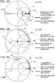
- FIG. 9A is an impedance diagram seen from the third reference plane toward the load.
- FIG. 9B is an impedance diagram seen from the first reference plane toward the load.
- FIG. 9C is an impedance diagram seen from the second reference plane toward the load.
- the load impedance is denoted by z L
- the characteristic impedance of the first impedance converting circuit 16 is denoted by z C1 .
- Use of a quarter-wave transformer enables the fundamental impedance z P3 to consist only of the resistance component at the center frequency f C . This facilitates designing the output matching circuit 20.
- the electrical length L1 of the first impedance converting circuit 16 is set to 0 degrees or more and 90 degrees or less so that the second harmonic impedance at the upper limit frequency f H seen from the first reference plane P1 toward the load is maintained to be inductive.
- the fundamental impedance z P1 is capacitive.
- FIG. 9C shows an impedance seen from the second reference plane P2 toward the load with the inductive reactance of the bonding wire 15 added thereto.
- the fundamental impedance z P2 at frequency f is the sum of the impedance z P1 seen from the first reference plane P1 toward the load and a reactance of 2 ⁇ f ⁇ Lw/Z CC resulting from the inductance Lw of the bonding wire 15.
- the fundamental impedance z P2 is matched with the output impedance z out of the semiconductor amplifying element 14.
- the electrical length L2 of the second impedance converting circuit 21 is set to a length corresponding to a quarter-wave transformer at the center frequency f C of the band of the amplifier.
- the fundamental impedance z P2 has a narrow locus region in the band and facilitates achieving a wide bandwidth.
- the second harmonic impedance z P22 is the sum of the second harmonic impedance z P12 kept inductive at the first reference plane P1 and a reactance of 4 ⁇ f ⁇ Lw/Z CC .
- the second harmonic impedance z P22 is made closer to the open-circuit impedance. Accordingly, the second harmonic can be confined in the semiconductor amplifying element 14 to increase the power added efficiency.
- TABLE 2 shows an example of the characteristic impedance and electrical length of the transmission line constituting the first impedance converting circuit 16 and the second impedance converting circuit 21.
- the characteristic impedance Z C2 of the transmission line constituting the second impedance converting circuit 21 is set to 18 ⁇ , and its electrical length L2 is set to 90 degrees at the center frequency f C .
- the characteristic impedance Z C1 of the transmission line constituting the first impedance converting circuit 16 is 2.4 ⁇ , and its electrical length L1 at the upper limit frequency f H is 90 degrees.
- the second impedance converting circuit 21 is made identical to that of the first case.
- the characteristic impedance Z C1 of the transmission line constituting the first impedance converting circuit 16 is 1.0 ⁇
- its electrical length L1 at the upper limit frequency f H is 22 degrees.
- the second impedance converting circuit 21 is made identical to that of the first case.
- the characteristic impedance Z C1 of the transmission line constituting the first impedance converting circuit 16 is 0.7 ⁇ , and its electrical length L1 at the upper limit frequency f H is 16 degrees.
- matching at the fundamental can be achieved by decreasing the characteristic impedance Z C1 of the first impedance converting circuit 16 and increasing the inductance Lw of the bonding wire 15 by the decreased amount of the first electrical length L1.
- the reflection coefficient for the second harmonic at the second reference plane P2 can be increased to 0.89 or more.
- FIG. 10 is a graph showing the dependence of characteristic impedance on transmission line width.
- the vertical axis represents characteristic impedance ( ⁇ ), and the horizontal axis represents line width (mm).
- the substrate constituting the microstrip line has a relative permittivity of 90 and a substrate thickness of 0.1 mm.
- the line width is preferably 4 mm or less. That is, the lower limit of the characteristic impedance is 1 ⁇ , as shown in TABLE 2.
- the electrical length L1 of the first impedance converting circuit 16 is preferably 22 degrees or more.
- FIG. 11 is a schematic view showing the configuration of a microwave semiconductor amplifier according to a fifth embodiment.
- the output matching circuit 20 of the microwave semiconductor amplifier according to the fifth embodiment further includes a third impedance converting circuit 22 cascaded to the second transmission line 21 of the fourth embodiment.
- the third impedance converting circuit 22 has a third characteristic impedance Z C3 higher than the second characteristic impedance Z C2 and an electrical length L3 of a quarter-wave impedance transformer at the center frequency f C of a prescribed frequency band.
- the third impedance converting circuit 22 is made of a third transmission line.
- the characteristic impedances are such that Z C1 ⁇ Z C2 ⁇ Z C3 ⁇ Z L .
- the electrical length L3 is set to 81 degrees or more and 99 degrees or less at the center frequency f C .
- the third impedance converting circuit 22 acts as a quarter-wave transformer.
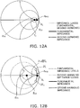
- FIG. 12A is an impedance diagram seen from the fourth reference plane toward the load.
- FIG. 12B is an impedance diagram seen from the third reference plane toward the load.
- the second impedance converting circuit 21 acts as a quarter-wave transformer.
- the fundamental impedance z P3 seen from the third reference plane P3 toward the load is generally a resistance, and can be set near the center of the impedance diagram.
- the second harmonic impedance z P32 is capacitive at twice the upper limit frequency of the frequency band.
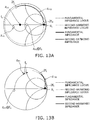
- FIG. 13A is an impedance diagram seen from the first reference plane toward the load.
- FIG. 13B is an impedance diagram seen from the second reference plane toward the load.
- the electrical length L1 of the first impedance converting circuit 16 is set to 90° or less.
- the second harmonic impedance z P12 seen from the first reference plane P1 is inductive, and does not become capacitive.
- FIG. 13B shows an impedance with the inductive impedance of the bonding wire 15 further added thereto.
- the impedance z P2 seen from the second reference plane P2 toward the load has small variation, and can ensure a wide bandwidth.
- the second harmonic impedance z P12 seen from the first reference plane P1 is kept inductive.
- the electrical length L1 at the upper limit frequency f H of the transmission line constituting the first impedance converting circuit 16 is preferably set to 22 degrees or more.
- FIG. 14 is a schematic view showing the configuration of a microwave semiconductor amplifier according to a sixth embodiment.
- the second impedance converting circuit 21 of the output matching circuit 20 includes a second transmission line 21a and a stub 21b.
- the second transmission line 21a has a characteristic impedance Z C2 and an electrical length L2 near 60 degrees at the center frequency f C .
- an electrical length near 60 degrees means 54 degrees or more and 66 degrees or less.
- the characteristic impedance Z C2 is higher than the characteristic impedance Z C1 and lower than the load impedance Z L .
- the output electrode of the semiconductor amplifying element 14 is connected to the first impedance converting circuit 16 by the bonding wire 15.
- the second reference plane P2 for seeing the impedance toward the load is defined as the bonding position on the output electrode of the semiconductor amplifying element 14.
- FIG. 15A is an impedance diagram seen from the third reference plane P3 toward the load.
- FIG. 15B is an impedance diagram seen from the first reference plane toward the load.
- FIG. 15C is an impedance diagram seen from the second reference plane toward the load.
- the load impedance is denoted by z L
- the characteristic impedance of the first impedance converting circuit 16 is denoted by z C1 .
- the fundamental impedance z P3 seen from the third reference plane P3 toward the load draws a clockwise locus along the dot-dashed line, and is converted to a low impedance.
- the second harmonic impedance z P32 draws a clockwise locus along the dotted line, and returns to nearly the original impedance.
- FIG. 15B shows an impedance seen from the first reference plane P1 toward the load.
- the first reference plane P1 is a connecting position between the first impedance converting circuit 16 and the bonding wire 15.
- the fundamental impedance z P3 at the third reference plane P3 is converted by the first impedance converting circuit 16 into z P1 at the first reference plane P1.
- the fundamental impedance z P1 at the center frequency f C moves as shown in FIG. 15B .
- the second harmonic impedance z P12 exhibits an inductive impedance near the outer periphery of the impedance diagram.
- FIG. 15C shows an impedance seen from the second reference plane P2 toward the load with the inductive reactance of the bonding wire 15 added thereto.
- the fundamental impedance z P2 at frequency f is the sum of the impedance z P1 seen from the first reference plane P1 toward the load and a reactance of 2 ⁇ f ⁇ Lw/Z CC resulting from the inductance Lw of the bonding wire 15.
- the second harmonic impedance z P22 is the sum of z P12 seen from the first reference plane P1 toward the load and a reactance of 4 ⁇ f ⁇ Lw/Z CC .
- the fundamental impedance z P2 has small variation in the band and exhibits a wide bandwidth.
- an inductive impedance is added to the second harmonic impedance z P12 kept inductive at the first reference plane P1.
- the second harmonic impedance z P22 is made closer to the open-circuit impedance while being maintained to be inductive. Accordingly, the second harmonic can be confined in the semiconductor amplifying element 14 to increase the power added efficiency.
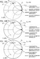
- FIGS. 16A to 16C are impedance diagrams seen from the third reference plane toward the load in the case of varying the characteristic impedance of the first impedance converting circuit 16 and its electrical length. More specifically, FIG. 16A is an impedance diagram in the first case. FIG. 16B is an impedance diagram in the second case. FIG. 16C is an impedance diagram in the third case.
- the first characteristic impedance Z C1 of the transmission line of the first impedance converting circuit 16 is set to 2.2 ⁇ , and the first electrical length L1 is set to 90 degrees at the upper limit frequency f H .
- the first characteristic impedance Z C1 of the transmission line of the first impedance converting circuit 16 is set to 1.0 ⁇ , and the first electrical length L1 is set to 27 degrees at the upper limit frequency f H .
- the first characteristic impedance Z C1 of the transmission line of the first impedance converting circuit 16 is set to 0.7 ⁇ , and the first electrical length L1 is set to 16 degrees at the upper limit frequency f H .
- the second impedance converting circuit 21 is common to all these cases.
- the characteristic impedance Z C2 of its transmission line 21a is set to 18 ⁇ , and the second electrical length L2 is set to 60 degrees at the center frequency f C . It is assumed that the second impedance converting circuit 21 further includes a stub 21b.
- the fundamental impedance z P3 draws a locus along the dot-dashed line, and is converted to a low impedance.
- the second harmonic impedance z P32 draws a locus along the dotted line, and returns to nearly the original impedance.
- FIGS. 17A to 17C are impedance diagrams seen from the first reference plane toward the load. More specifically, FIG. 17A is an impedance diagram in the first case. FIG. 17B is an impedance diagram in the second case. FIG. 17C is an impedance diagram in the third case.
- FIGS. 18A to 18C are impedance diagrams seen from the second reference plane toward the load. More specifically, FIG. 18A is an impedance diagram in the first case. FIG. 18B is an impedance diagram in the second case. FIG. 18C is an impedance diagram in the third case.
- the impedance z P1 at the first reference plane P1 is preferably located on the constant resistance circle g1, g2, g3 for the complex conjugate of the output impedance z out of the semiconductor amplifying element 14. TABLE 3 lists these results.
- the first electrical length L1 of the first impedance converting circuit 16 is decreased, matching can be achieved at the fundamental by decreasing the characteristic impedance Z C1 of the first impedance converting circuit 16 and increasing the inductance Lw of the bonding wire 15.
- the reflection coefficient ⁇ for the second harmonic at the second reference plane P2 can be increased to 0.99 or more.
- the lower limit of the characteristic impedance is 1 ⁇ from TABLE 3.
- the first electrical length L1 of the first impedance converting circuit 16 is set to 27 degrees or more.
- the reflection coefficient ⁇ at the second reference plane P2 of the semiconductor amplifying element 14 can be set to 0.97 or more.
- the impedance for the second harmonic can be sufficiently increased.
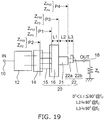
- FIG. 19 is a schematic view showing the configuration of a microwave semiconductor amplifier according to a seventh embodiment.
- the output matching circuit 20 of the microwave semiconductor amplifier according to the seventh embodiment further includes a third impedance converting circuit 22 cascaded to the second impedance converting circuit 21 and made of a third transmission line.
- the second impedance converting circuit 21 is made of a second transmission line having a characteristic impedance Z C2 and a second electrical length L2.
- the third impedance converting circuit 22 includes a transmission line 22a having a characteristic impedance Z C3 and a third electrical length L3, and a stub 22b connected to the transmission line 22a.
- the second electrical length L2 of the second impedance converting circuit 21 and the third electrical length L3 of the transmission line 22a of the third impedance converting circuit 22 are set to a length corresponding to a quarter-wave transformer at the center frequency f C .
- Z C1 ⁇ Z C2 ⁇ Z C3 ⁇ Z L it is assumed that Z C1 ⁇ Z C2 ⁇ Z C3 ⁇ Z L .
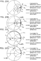
- FIG. 20A is an impedance diagram seen from the fourth reference plane toward the load.
- FIG. 20B is an impedance diagram seen from the third reference plane toward the load.
- FIG. 20C is an impedance diagram seen from the first reference plane toward the load.
- FIG. 20D is an impedance diagram seen from the second reference plane toward the load.
- the fundamental impedance z P4 seen from the fourth reference plane P4 toward the load is converted by the third impedance converting circuit 22.
- the second impedance converting circuit 21 acts as a quarter-wave transformer to perform impedance conversion.
- the impedance z P3 converted by the quarter-wave transformer becomes a resistance and can be represented by the following equation.
- z P3 z C2 2 / z P4
- FIG. 20C shows a fundamental impedance z P1 seen from the first reference plane P1 toward the load.
- the second harmonic impedance z P12 seen from the first reference plane P1 toward the load is inductive.
- FIG. 20D shows a fundamental impedance z P2 and a second harmonic impedance z P22 seen from the second reference plane P2 toward the load with the reactance resulting from the inductance Lw of the bonding wire 15 added thereto.
- the second harmonic impedance seen from the first reference plane P1 is kept inductive.
- the electrical length L1 at the upper limit frequency f H of the transmission line constituting the first impedance converting circuit 16 is preferably set to 27 degrees or more.
- a higher harmonic processing circuit cascaded with a matching circuit is provided on the output side near the semiconductor amplifying element.
- the power added efficiency is increased.
- the higher harmonic processing circuit is not used. Instead, an impedance converting circuit made of a transmission line is connected on the output side of the semiconductor amplifying element 14.
- the fundamental impedance and the second harmonic impedance can be separately converted to a desired range.
- the fundamental impedance is matched with the output impedance z out of the semiconductor amplifying element 14.
- the first to seventh embodiments provide a microwave semiconductor amplifier capable of achieving high power added efficiency and wide bandwidth.
- a microwave semiconductor amplifier can be widely used in radio communication devices, mobile communication base stations, radar devices and the like at radio frequencies of 1 GHz or more.
Landscapes
- Engineering & Computer Science (AREA)
- Power Engineering (AREA)
- Microwave Amplifiers (AREA)
Claims (13)
- Mikrowellenhalbleiterverstärker mit einem Ausgangsanschluss (18), verbunden mit einer externen Last, wobei der Verstärker ein vorgeschriebenes Frequenzband aufweist, umfassend:ein Halbleiterverstärkungselement (14), eine Eingangselektrode und eine Ausgangselektrode enthaltend und eine kapazitive Ausgangsimpedanz in dem Frequenzband aufweisend;eine Eingangsanpassungsschaltung (12), verbunden mit der Eingangselektrode;
undeine Ausgangsanpassungsschaltung (20), enthaltend einen Kontaktierdraht (15) und eine erste Übertragungsleitung (16), wobei der Kontaktierdraht (15) einen ersten Endabschnitt und einen zweiten Endabschnitt an einem gegenüberliegenden Ende des ersten Endabschnitts enthält, wobei der erste Endabschnitt mit der Ausgangselektrode verbunden ist, der zweite Endabschnitt mit einem Endabschnitt der ersten Übertragungsleitung (16) verbunden ist, die erste Übertragungsleitung (16) zu dem Ausgangsanschluss (18) in Kaskade geschaltet ist, die erste Übertragungsleitung eine erste charakteristische Impedanz und eine erste elektrische Länge von 90 Grad oder weniger an einer oberen Grenzfrequenz aufweist,die Ausgangsanpassungsschaltung (20) die kapazitive Ausgangsimpedanz des Halbleiterverstärkungselements (14) an eine Grundimpedanz der externen Last durch Hinzufügen einer induktiven Reaktanz des Kontaktierdrahts (15) zu einer Grundimpedanz, gesehen hin zur externen Last von dem einen Endabschnitt der ersten Übertragungsleitung (16), anpasst, undeine zweite harmonische Impedanz, gesehen von dem Ausgang hin zur externen Last von dem Halbleiterverstärkungselement (14), näher an eine Leerlaufimpedanz durch Hinzufügen einer induktiven Reaktanz des Kontaktierdrahts (15) zu einer induktiven zweiten harmonischen Impedanz, gesehen hin zur externen Last von dem einen Endabschnitt der ersten Übertragungsleitung (16) innerhalb eines Frequenzbereichs vom Doppelten einer unteren Grenzfrequenz des Frequenzbands zum Doppelten einer oberen Grenzfrequenz des Frequenzbands gemacht wird. - Verstärker nach Anspruch 1, wobei
die Ausgangsanpassungsschaltung (20) ferner eine zweite Übertragungsleitung (21) enthält, die eine zweite charakteristische Impedanz höher als die erste charakteristische Impedanz und eine zweite elektrische Länge von 90 Grad oder weniger an der oberen Grenzfrequenz aufweist und
die zweite Übertragungsleitung (21) zwischen der ersten Übertragungsleitung (16) und dem Ausgangsanschluss (18) bereitgestellt ist. - Verstärker nach Anspruch 2, wobei die zweite elektrische Länge 60 Grad oder mehr an der unteren Grenzfrequenz des Frequenzbands beträgt.
- Verstärker nach Anspruch 2, wobei
die Ausgangsanpassungsschaltung (20) ferner eine dritte Übertragungsleitung (22) enthält, die eine dritte charakteristische Impedanz höher als die zweite charakteristische Impedanz und eine dritte elektrische Länge von 90 Grad oder weniger an der oberen Grenzfrequenz aufweist und
die dritte Übertragungsleitung (22) zwischen der zweiten Übertragungsleitung (21) und dem Ausgangsanschluss (18) bereitgestellt ist. - Verstärker nach Anspruch 4, wobei die dritte elektrische Länge 60 Grad oder mehr an der unteren Grenzfrequenz des Frequenzbands beträgt.
- Verstärker nach Anspruch 1, wobei die Ausgangsanpassungsschaltung (20) ferner eine zweite Übertragungsleitung (21) enthält, die eine zweite charakteristische Impedanz höher als die erste charakteristische Impedanz aufweist, in Kaskade geschaltet zu der ersten Übertragungsleitung (16), und eine zweite elektrische Länge, die als ein Viertelwellen-Transformator an einer Mittenfrequenz des Frequenzbands wirkt, aufweist.
- Verstärker nach Anspruch 6, wobei die Ausgangsanpassungsschaltung (20) ferner eine dritte Übertragungsleitung (22) enthält, in Kaskade geschaltet zu der zweiten Übertragungsleitung (21) und eine dritte charakteristische Impedanz höher als die zweite charakteristische Impedanz und eine dritte elektrische Länge, die als ein Viertelwellen-Transformator an der Mittenfrequenz des Frequenzbands wirkt, aufweisend.
- Verstärker nach Anspruch 6 oder 7, wobei die erste elektrische Länge 22 Grad oder mehr an der oberen Grenzfrequenz beträgt.
- Verstärker nach Anspruch 1, wobei die Ausgangsanpassungsschaltung (20) ferner eine zweite Übertragungsleitung (21a) enthält, in Kaskade geschaltet zu der ersten Übertragungsleitung (16), und eine Stichleitung (21b), verbunden mit der zweiten Übertragungsleitung (21a), und die kapazitive Ausgangsimpedanz des Halbleiterverstärkungselements an die Grundimpedanz der externen Last anpasst.
- Verstärker nach Anspruch 9, wobei
die zweite Übertragungsleitung (21a) eine zweite charakteristische Impedanz höher als die erste charakteristische Impedanz und eine elektrische Länge von 51 Grad oder mehr und 69 Grad oder weniger an einer Mittenfrequenz des Frequenzbands aufweist. - Verstärker nach Anspruch 1, wobei die Ausgangsanpassungsschaltung (20) ferner eine zweite Übertragungsleitung (21) enthält, in Kaskade geschaltet zu der ersten Übertragungsleitung (16), eine dritte Übertragungsleitung (22a), in Kaskade geschaltet zu der zweiten Übertragungsleitung (21), und eine Stichleitung (22b), verbunden mit der dritten Übertragungsleitung (22a), und die kapazitive Ausgangsimpedanz des Halbleiterverstärkungselements an die Grundimpedanz der externen Last anpasst.
- Verstärker nach Anspruch 11, wobei
die zweite Übertragungsleitung (21) eine zweite charakteristische Impedanz höher als die erste charakteristische Impedanz und eine zweite elektrische Länge, die als ein Viertelwellen-Transformator an einer Mittenfrequenz des Frequenzbands wirkt, aufweist
und
die dritte Übertragungsleitung (22a) eine dritte charakteristische Impedanz höher als die zweite charakteristische Impedanz und eine elektrische Länge, die als ein Viertelwellen-Transformator an der Mittenfrequenz des Frequenzbands wirkt, aufweist. - Verstärker nach Anspruch 10 oder 12, wobei
die erste charakteristische Impedanz 1 Ω oder mehr beträgt und
die erste elektrische Länge 27 Grad oder mehr an der oberen Grenzfrequenz des Frequenzbands beträgt.
Applications Claiming Priority (3)
| Application Number | Priority Date | Filing Date | Title |
|---|---|---|---|
| JP2012052195A JP5603893B2 (ja) | 2012-03-08 | 2012-03-08 | 高周波半導体増幅器 |
| JP2012052197A JP5468095B2 (ja) | 2012-03-08 | 2012-03-08 | 高周波半導体増幅器 |
| JP2012052196A JP5619055B2 (ja) | 2012-03-08 | 2012-03-08 | 高周波半導体増幅器 |
Publications (2)
| Publication Number | Publication Date |
|---|---|
| EP2637302A1 EP2637302A1 (de) | 2013-09-11 |
| EP2637302B1 true EP2637302B1 (de) | 2018-03-28 |
Family
ID=47563119
Family Applications (1)
| Application Number | Title | Priority Date | Filing Date |
|---|---|---|---|
| EP12199817.3A Active EP2637302B1 (de) | 2012-03-08 | 2012-12-31 | Mikrowellen-Halbleiterverstärker |
Country Status (2)
| Country | Link |
|---|---|
| US (1) | US9035702B2 (de) |
| EP (1) | EP2637302B1 (de) |
Families Citing this family (9)
| Publication number | Priority date | Publication date | Assignee | Title |
|---|---|---|---|---|
| US8988161B2 (en) * | 2013-06-20 | 2015-03-24 | Triquint Semiconductor, Inc. | Transformer for monolithic microwave integrated circuits |
| JP6383224B2 (ja) | 2014-09-08 | 2018-08-29 | 株式会社東芝 | 半導体増幅器 |
| JP6049673B2 (ja) | 2014-10-31 | 2016-12-21 | 株式会社東芝 | 半導体増幅装置 |
| JP6189881B2 (ja) | 2015-01-27 | 2017-08-30 | 株式会社東芝 | 高周波半導体増幅器 |
| JP6189880B2 (ja) * | 2015-01-27 | 2017-08-30 | 株式会社東芝 | 高周波半導体増幅器 |
| JP6190399B2 (ja) | 2015-01-28 | 2017-08-30 | 株式会社東芝 | 高周波半導体増幅器 |
| JP6109868B2 (ja) | 2015-03-06 | 2017-04-05 | 株式会社東芝 | 高周波増幅器 |
| JP6523108B2 (ja) * | 2015-09-08 | 2019-05-29 | 株式会社東芝 | 高周波半導体増幅器 |
| CN107834139A (zh) * | 2017-10-20 | 2018-03-23 | 绵阳鑫阳知识产权运营有限公司 | 一种低噪声放大器的传输线结构 |
Family Cites Families (15)
| Publication number | Priority date | Publication date | Assignee | Title |
|---|---|---|---|---|
| US4390851A (en) * | 1980-11-25 | 1983-06-28 | Rockwell International Corporation | Monolithic microwave amplifier having active impedance matching |
| US4476446A (en) * | 1981-08-25 | 1984-10-09 | Raytheon Company | Impedance matching network for field effect transistor |
| JPH0785528B2 (ja) * | 1989-12-25 | 1995-09-13 | 日本電気株式会社 | 高出力マイクロ波ミリ波トランジスタ安定化回路 |
| JPH0738548B2 (ja) | 1993-01-07 | 1995-04-26 | 日本電気株式会社 | 電力整合回路 |
| JP3668610B2 (ja) * | 1998-04-10 | 2005-07-06 | 太陽誘電株式会社 | 高周波電力増幅回路 |
| TW473882B (en) | 1998-07-06 | 2002-01-21 | Hitachi Ltd | Semiconductor device |
| WO2000075990A1 (en) | 1999-06-07 | 2000-12-14 | Ericsson Inc. | High impedance matched rf power transistor |
| JP2003282721A (ja) | 2002-03-26 | 2003-10-03 | Murata Mfg Co Ltd | 半導体装置および送受信装置 |
| JP2004228989A (ja) * | 2003-01-23 | 2004-08-12 | Renesas Technology Corp | 半導体装置 |
| JP5085179B2 (ja) | 2007-04-12 | 2012-11-28 | 株式会社東芝 | F級増幅回路 |
| JP5056480B2 (ja) | 2008-02-29 | 2012-10-24 | 三菱電機株式会社 | 高周波半導体増幅器 |
| JP5424790B2 (ja) | 2009-09-18 | 2014-02-26 | 三菱電機株式会社 | 高出力増幅器 |
| JP5450479B2 (ja) | 2011-02-28 | 2014-03-26 | 株式会社東芝 | Ab級増幅器 |
| JP5367744B2 (ja) | 2011-02-28 | 2013-12-11 | 株式会社東芝 | Ab級増幅器 |
| JP5367743B2 (ja) | 2011-02-28 | 2013-12-11 | 株式会社東芝 | C級増幅器 |
-
2012
- 2012-12-27 US US13/728,167 patent/US9035702B2/en active Active
- 2012-12-31 EP EP12199817.3A patent/EP2637302B1/de active Active
Non-Patent Citations (1)
| Title |
|---|
| None * |
Also Published As
| Publication number | Publication date |
|---|---|
| US9035702B2 (en) | 2015-05-19 |
| US20130234794A1 (en) | 2013-09-12 |
| EP2637302A1 (de) | 2013-09-11 |
Similar Documents
| Publication | Publication Date | Title |
|---|---|---|
| EP2637302B1 (de) | Mikrowellen-Halbleiterverstärker | |
| JP5603893B2 (ja) | 高周波半導体増幅器 | |
| Kang et al. | Octave bandwidth Doherty power amplifier using multiple resonance circuit for the peaking amplifier | |
| JP5619055B2 (ja) | 高周波半導体増幅器 | |
| CN108233881B (zh) | 放大器电路和经封装的放大器电路 | |
| US10424841B2 (en) | Antenna matching circuit, antenna circuit, front-end circuit, and communication apparatus | |
| EP3662577B1 (de) | Harmonisches breitbandanpassungsnetzwerk | |
| US7567128B2 (en) | Power amplifier suppressing radiation of second harmonic over wide frequency band | |
| JP5468095B2 (ja) | 高周波半導体増幅器 | |
| US8988161B2 (en) | Transformer for monolithic microwave integrated circuits | |
| US10453810B2 (en) | Integrated passive device for RF power amplifier package | |
| JP2015149626A (ja) | 高周波半導体増幅器 | |
| US9590562B2 (en) | Semiconductor amplifier bias circuit and semiconductor amplifier device | |
| CN116131781A (zh) | 功率放大器 | |
| JP2011199338A (ja) | 増幅器 | |
| JP6523108B2 (ja) | 高周波半導体増幅器 | |
| Ko et al. | A 0.4-1.2 GHz Reconfigurable CMOS Power Amplifier for 802.11 ah/af Applications | |
| JP2004140438A (ja) | 周波数変換回路 | |
| Lakhssassi | Design of LS band broadband power amplifier using microstip lines | |
| JP2013219484A (ja) | 高周波半導体増幅器 | |
| Kim et al. | Wideband approach of the fully integrated transmitter front-end with high power-added efficiency |
Legal Events
| Date | Code | Title | Description |
|---|---|---|---|
| PUAI | Public reference made under article 153(3) epc to a published international application that has entered the european phase |
Free format text: ORIGINAL CODE: 0009012 |
|
| 17P | Request for examination filed |
Effective date: 20121231 |
|
| AK | Designated contracting states |
Kind code of ref document: A1 Designated state(s): AL AT BE BG CH CY CZ DE DK EE ES FI FR GB GR HR HU IE IS IT LI LT LU LV MC MK MT NL NO PL PT RO RS SE SI SK SM TR |
|
| AX | Request for extension of the european patent |
Extension state: BA ME |
|
| 17Q | First examination report despatched |
Effective date: 20140430 |
|
| GRAP | Despatch of communication of intention to grant a patent |
Free format text: ORIGINAL CODE: EPIDOSNIGR1 |
|
| STAA | Information on the status of an ep patent application or granted ep patent |
Free format text: STATUS: GRANT OF PATENT IS INTENDED |
|
| INTG | Intention to grant announced |
Effective date: 20171011 |
|
| GRAS | Grant fee paid |
Free format text: ORIGINAL CODE: EPIDOSNIGR3 |
|
| GRAA | (expected) grant |
Free format text: ORIGINAL CODE: 0009210 |
|
| STAA | Information on the status of an ep patent application or granted ep patent |
Free format text: STATUS: THE PATENT HAS BEEN GRANTED |
|
| AK | Designated contracting states |
Kind code of ref document: B1 Designated state(s): AL AT BE BG CH CY CZ DE DK EE ES FI FR GB GR HR HU IE IS IT LI LT LU LV MC MK MT NL NO PL PT RO RS SE SI SK SM TR |
|
| REG | Reference to a national code |
Ref country code: GB Ref legal event code: FG4D |
|
| REG | Reference to a national code |
Ref country code: CH Ref legal event code: EP |
|
| REG | Reference to a national code |
Ref country code: AT Ref legal event code: REF Ref document number: 984273 Country of ref document: AT Kind code of ref document: T Effective date: 20180415 |
|
| REG | Reference to a national code |
Ref country code: IE Ref legal event code: FG4D |
|
| REG | Reference to a national code |
Ref country code: DE Ref legal event code: R096 Ref document number: 602012044434 Country of ref document: DE |
|
| PG25 | Lapsed in a contracting state [announced via postgrant information from national office to epo] |
Ref country code: NO Free format text: LAPSE BECAUSE OF FAILURE TO SUBMIT A TRANSLATION OF THE DESCRIPTION OR TO PAY THE FEE WITHIN THE PRESCRIBED TIME-LIMIT Effective date: 20180628 Ref country code: HR Free format text: LAPSE BECAUSE OF FAILURE TO SUBMIT A TRANSLATION OF THE DESCRIPTION OR TO PAY THE FEE WITHIN THE PRESCRIBED TIME-LIMIT Effective date: 20180328 Ref country code: LT Free format text: LAPSE BECAUSE OF FAILURE TO SUBMIT A TRANSLATION OF THE DESCRIPTION OR TO PAY THE FEE WITHIN THE PRESCRIBED TIME-LIMIT Effective date: 20180328 Ref country code: FI Free format text: LAPSE BECAUSE OF FAILURE TO SUBMIT A TRANSLATION OF THE DESCRIPTION OR TO PAY THE FEE WITHIN THE PRESCRIBED TIME-LIMIT Effective date: 20180328 |
|
| REG | Reference to a national code |
Ref country code: NL Ref legal event code: MP Effective date: 20180328 |
|
| REG | Reference to a national code |
Ref country code: LT Ref legal event code: MG4D |
|
| PG25 | Lapsed in a contracting state [announced via postgrant information from national office to epo] |
Ref country code: GR Free format text: LAPSE BECAUSE OF FAILURE TO SUBMIT A TRANSLATION OF THE DESCRIPTION OR TO PAY THE FEE WITHIN THE PRESCRIBED TIME-LIMIT Effective date: 20180629 Ref country code: LV Free format text: LAPSE BECAUSE OF FAILURE TO SUBMIT A TRANSLATION OF THE DESCRIPTION OR TO PAY THE FEE WITHIN THE PRESCRIBED TIME-LIMIT Effective date: 20180328 Ref country code: RS Free format text: LAPSE BECAUSE OF FAILURE TO SUBMIT A TRANSLATION OF THE DESCRIPTION OR TO PAY THE FEE WITHIN THE PRESCRIBED TIME-LIMIT Effective date: 20180328 Ref country code: SE Free format text: LAPSE BECAUSE OF FAILURE TO SUBMIT A TRANSLATION OF THE DESCRIPTION OR TO PAY THE FEE WITHIN THE PRESCRIBED TIME-LIMIT Effective date: 20180328 Ref country code: BG Free format text: LAPSE BECAUSE OF FAILURE TO SUBMIT A TRANSLATION OF THE DESCRIPTION OR TO PAY THE FEE WITHIN THE PRESCRIBED TIME-LIMIT Effective date: 20180628 |
|
| PG25 | Lapsed in a contracting state [announced via postgrant information from national office to epo] |
Ref country code: IT Free format text: LAPSE BECAUSE OF FAILURE TO SUBMIT A TRANSLATION OF THE DESCRIPTION OR TO PAY THE FEE WITHIN THE PRESCRIBED TIME-LIMIT Effective date: 20180328 Ref country code: EE Free format text: LAPSE BECAUSE OF FAILURE TO SUBMIT A TRANSLATION OF THE DESCRIPTION OR TO PAY THE FEE WITHIN THE PRESCRIBED TIME-LIMIT Effective date: 20180328 Ref country code: ES Free format text: LAPSE BECAUSE OF FAILURE TO SUBMIT A TRANSLATION OF THE DESCRIPTION OR TO PAY THE FEE WITHIN THE PRESCRIBED TIME-LIMIT Effective date: 20180328 Ref country code: AL Free format text: LAPSE BECAUSE OF FAILURE TO SUBMIT A TRANSLATION OF THE DESCRIPTION OR TO PAY THE FEE WITHIN THE PRESCRIBED TIME-LIMIT Effective date: 20180328 Ref country code: PL Free format text: LAPSE BECAUSE OF FAILURE TO SUBMIT A TRANSLATION OF THE DESCRIPTION OR TO PAY THE FEE WITHIN THE PRESCRIBED TIME-LIMIT Effective date: 20180328 Ref country code: RO Free format text: LAPSE BECAUSE OF FAILURE TO SUBMIT A TRANSLATION OF THE DESCRIPTION OR TO PAY THE FEE WITHIN THE PRESCRIBED TIME-LIMIT Effective date: 20180328 Ref country code: NL Free format text: LAPSE BECAUSE OF FAILURE TO SUBMIT A TRANSLATION OF THE DESCRIPTION OR TO PAY THE FEE WITHIN THE PRESCRIBED TIME-LIMIT Effective date: 20180328 |
|
| PG25 | Lapsed in a contracting state [announced via postgrant information from national office to epo] |
Ref country code: CZ Free format text: LAPSE BECAUSE OF FAILURE TO SUBMIT A TRANSLATION OF THE DESCRIPTION OR TO PAY THE FEE WITHIN THE PRESCRIBED TIME-LIMIT Effective date: 20180328 Ref country code: SK Free format text: LAPSE BECAUSE OF FAILURE TO SUBMIT A TRANSLATION OF THE DESCRIPTION OR TO PAY THE FEE WITHIN THE PRESCRIBED TIME-LIMIT Effective date: 20180328 Ref country code: SM Free format text: LAPSE BECAUSE OF FAILURE TO SUBMIT A TRANSLATION OF THE DESCRIPTION OR TO PAY THE FEE WITHIN THE PRESCRIBED TIME-LIMIT Effective date: 20180328 |
|
| REG | Reference to a national code |
Ref country code: AT Ref legal event code: MK05 Ref document number: 984273 Country of ref document: AT Kind code of ref document: T Effective date: 20180328 |
|
| PG25 | Lapsed in a contracting state [announced via postgrant information from national office to epo] |
Ref country code: PT Free format text: LAPSE BECAUSE OF FAILURE TO SUBMIT A TRANSLATION OF THE DESCRIPTION OR TO PAY THE FEE WITHIN THE PRESCRIBED TIME-LIMIT Effective date: 20180730 |
|
| REG | Reference to a national code |
Ref country code: DE Ref legal event code: R097 Ref document number: 602012044434 Country of ref document: DE |
|
| PG25 | Lapsed in a contracting state [announced via postgrant information from national office to epo] |
Ref country code: DK Free format text: LAPSE BECAUSE OF FAILURE TO SUBMIT A TRANSLATION OF THE DESCRIPTION OR TO PAY THE FEE WITHIN THE PRESCRIBED TIME-LIMIT Effective date: 20180328 Ref country code: AT Free format text: LAPSE BECAUSE OF FAILURE TO SUBMIT A TRANSLATION OF THE DESCRIPTION OR TO PAY THE FEE WITHIN THE PRESCRIBED TIME-LIMIT Effective date: 20180328 |
|
| PLBE | No opposition filed within time limit |
Free format text: ORIGINAL CODE: 0009261 |
|
| STAA | Information on the status of an ep patent application or granted ep patent |
Free format text: STATUS: NO OPPOSITION FILED WITHIN TIME LIMIT |
|
| 26N | No opposition filed |
Effective date: 20190103 |
|
| PG25 | Lapsed in a contracting state [announced via postgrant information from national office to epo] |
Ref country code: SI Free format text: LAPSE BECAUSE OF FAILURE TO SUBMIT A TRANSLATION OF THE DESCRIPTION OR TO PAY THE FEE WITHIN THE PRESCRIBED TIME-LIMIT Effective date: 20180328 |
|
| REG | Reference to a national code |
Ref country code: CH Ref legal event code: PL |
|
| PG25 | Lapsed in a contracting state [announced via postgrant information from national office to epo] |
Ref country code: MC Free format text: LAPSE BECAUSE OF FAILURE TO SUBMIT A TRANSLATION OF THE DESCRIPTION OR TO PAY THE FEE WITHIN THE PRESCRIBED TIME-LIMIT Effective date: 20180328 Ref country code: LU Free format text: LAPSE BECAUSE OF NON-PAYMENT OF DUE FEES Effective date: 20181231 |
|
| REG | Reference to a national code |
Ref country code: BE Ref legal event code: MM Effective date: 20181231 Ref country code: IE Ref legal event code: MM4A |
|
| PG25 | Lapsed in a contracting state [announced via postgrant information from national office to epo] |
Ref country code: IE Free format text: LAPSE BECAUSE OF NON-PAYMENT OF DUE FEES Effective date: 20181231 |
|
| PG25 | Lapsed in a contracting state [announced via postgrant information from national office to epo] |
Ref country code: BE Free format text: LAPSE BECAUSE OF NON-PAYMENT OF DUE FEES Effective date: 20181231 |
|
| PG25 | Lapsed in a contracting state [announced via postgrant information from national office to epo] |
Ref country code: CH Free format text: LAPSE BECAUSE OF NON-PAYMENT OF DUE FEES Effective date: 20181231 Ref country code: LI Free format text: LAPSE BECAUSE OF NON-PAYMENT OF DUE FEES Effective date: 20181231 |
|
| PG25 | Lapsed in a contracting state [announced via postgrant information from national office to epo] |
Ref country code: MT Free format text: LAPSE BECAUSE OF NON-PAYMENT OF DUE FEES Effective date: 20181231 |
|
| PG25 | Lapsed in a contracting state [announced via postgrant information from national office to epo] |
Ref country code: TR Free format text: LAPSE BECAUSE OF FAILURE TO SUBMIT A TRANSLATION OF THE DESCRIPTION OR TO PAY THE FEE WITHIN THE PRESCRIBED TIME-LIMIT Effective date: 20180328 |
|
| PG25 | Lapsed in a contracting state [announced via postgrant information from national office to epo] |
Ref country code: HU Free format text: LAPSE BECAUSE OF FAILURE TO SUBMIT A TRANSLATION OF THE DESCRIPTION OR TO PAY THE FEE WITHIN THE PRESCRIBED TIME-LIMIT; INVALID AB INITIO Effective date: 20121231 Ref country code: CY Free format text: LAPSE BECAUSE OF FAILURE TO SUBMIT A TRANSLATION OF THE DESCRIPTION OR TO PAY THE FEE WITHIN THE PRESCRIBED TIME-LIMIT Effective date: 20180328 Ref country code: MK Free format text: LAPSE BECAUSE OF NON-PAYMENT OF DUE FEES Effective date: 20180328 |
|
| PG25 | Lapsed in a contracting state [announced via postgrant information from national office to epo] |
Ref country code: IS Free format text: LAPSE BECAUSE OF FAILURE TO SUBMIT A TRANSLATION OF THE DESCRIPTION OR TO PAY THE FEE WITHIN THE PRESCRIBED TIME-LIMIT Effective date: 20180728 |
|
| PGFP | Annual fee paid to national office [announced via postgrant information from national office to epo] |
Ref country code: DE Payment date: 20251104 Year of fee payment: 14 |
|
| PGFP | Annual fee paid to national office [announced via postgrant information from national office to epo] |
Ref country code: GB Payment date: 20251114 Year of fee payment: 14 |
|
| PGFP | Annual fee paid to national office [announced via postgrant information from national office to epo] |
Ref country code: FR Payment date: 20251110 Year of fee payment: 14 |