EP2637400A2 - Capteur d'image et procédé de capture d'une image - Google Patents
Capteur d'image et procédé de capture d'une image Download PDFInfo
- Publication number
- EP2637400A2 EP2637400A2 EP13157643.1A EP13157643A EP2637400A2 EP 2637400 A2 EP2637400 A2 EP 2637400A2 EP 13157643 A EP13157643 A EP 13157643A EP 2637400 A2 EP2637400 A2 EP 2637400A2
- Authority
- EP
- European Patent Office
- Prior art keywords
- counter
- photodiode
- photodiodes
- light
- image
- Prior art date
- Legal status (The legal status is an assumption and is not a legal conclusion. Google has not performed a legal analysis and makes no representation as to the accuracy of the status listed.)
- Ceased
Links
- 238000000034 method Methods 0.000 title claims description 7
- 239000000758 substrate Substances 0.000 claims abstract description 17
- 238000012545 processing Methods 0.000 claims abstract description 11
- 238000011156 evaluation Methods 0.000 claims abstract description 9
- 230000000007 visual effect Effects 0.000 claims abstract description 8
- 230000003287 optical effect Effects 0.000 claims abstract description 6
- 230000015654 memory Effects 0.000 claims description 6
- 238000003384 imaging method Methods 0.000 claims description 2
- 238000003491 array Methods 0.000 claims 1
- 238000013461 design Methods 0.000 description 4
- 230000007423 decrease Effects 0.000 description 2
- 230000010354 integration Effects 0.000 description 2
- 241001295925 Gegenes Species 0.000 description 1
- 238000006243 chemical reaction Methods 0.000 description 1
- 238000010586 diagram Methods 0.000 description 1
- 238000009434 installation Methods 0.000 description 1
- 230000003071 parasitic effect Effects 0.000 description 1
- 230000035945 sensitivity Effects 0.000 description 1
- 230000001360 synchronised effect Effects 0.000 description 1
- 238000012546 transfer Methods 0.000 description 1
Images


Classifications
-
- H—ELECTRICITY
- H10—SEMICONDUCTOR DEVICES; ELECTRIC SOLID-STATE DEVICES NOT OTHERWISE PROVIDED FOR
- H10F—INORGANIC SEMICONDUCTOR DEVICES SENSITIVE TO INFRARED RADIATION, LIGHT, ELECTROMAGNETIC RADIATION OF SHORTER WAVELENGTH OR CORPUSCULAR RADIATION
- H10F39/00—Integrated devices, or assemblies of multiple devices, comprising at least one element covered by group H10F30/00, e.g. radiation detectors comprising photodiode arrays
- H10F39/10—Integrated devices
- H10F39/103—Integrated devices the at least one element covered by H10F30/00 having potential barriers, e.g. integrated devices comprising photodiodes or phototransistors
-
- H—ELECTRICITY
- H04—ELECTRIC COMMUNICATION TECHNIQUE
- H04N—PICTORIAL COMMUNICATION, e.g. TELEVISION
- H04N25/00—Circuitry of solid-state image sensors [SSIS]; Control thereof
- H04N25/40—Extracting pixel data from image sensors by controlling scanning circuits, e.g. by modifying the number of pixels sampled or to be sampled
- H04N25/41—Extracting pixel data from a plurality of image sensors simultaneously picking up an image, e.g. for increasing the field of view by combining the outputs of a plurality of sensors
-
- H—ELECTRICITY
- H04—ELECTRIC COMMUNICATION TECHNIQUE
- H04N—PICTORIAL COMMUNICATION, e.g. TELEVISION
- H04N25/00—Circuitry of solid-state image sensors [SSIS]; Control thereof
- H04N25/70—SSIS architectures; Circuits associated therewith
-
- H—ELECTRICITY
- H04—ELECTRIC COMMUNICATION TECHNIQUE
- H04N—PICTORIAL COMMUNICATION, e.g. TELEVISION
- H04N25/00—Circuitry of solid-state image sensors [SSIS]; Control thereof
- H04N25/70—SSIS architectures; Circuits associated therewith
- H04N25/76—Addressed sensors, e.g. MOS or CMOS sensors
- H04N25/77—Pixel circuitry, e.g. memories, A/D converters, pixel amplifiers, shared circuits or shared components
-
- H—ELECTRICITY
- H04—ELECTRIC COMMUNICATION TECHNIQUE
- H04N—PICTORIAL COMMUNICATION, e.g. TELEVISION
- H04N25/00—Circuitry of solid-state image sensors [SSIS]; Control thereof
- H04N25/70—SSIS architectures; Circuits associated therewith
- H04N25/76—Addressed sensors, e.g. MOS or CMOS sensors
- H04N25/77—Pixel circuitry, e.g. memories, A/D converters, pixel amplifiers, shared circuits or shared components
- H04N25/772—Pixel circuitry, e.g. memories, A/D converters, pixel amplifiers, shared circuits or shared components comprising A/D, V/T, V/F, I/T or I/F converters
-
- H—ELECTRICITY
- H04—ELECTRIC COMMUNICATION TECHNIQUE
- H04N—PICTORIAL COMMUNICATION, e.g. TELEVISION
- H04N25/00—Circuitry of solid-state image sensors [SSIS]; Control thereof
- H04N25/70—SSIS architectures; Circuits associated therewith
- H04N25/76—Addressed sensors, e.g. MOS or CMOS sensors
- H04N25/78—Readout circuits for addressed sensors, e.g. output amplifiers or A/D converters
-
- H—ELECTRICITY
- H10—SEMICONDUCTOR DEVICES; ELECTRIC SOLID-STATE DEVICES NOT OTHERWISE PROVIDED FOR
- H10F—INORGANIC SEMICONDUCTOR DEVICES SENSITIVE TO INFRARED RADIATION, LIGHT, ELECTROMAGNETIC RADIATION OF SHORTER WAVELENGTH OR CORPUSCULAR RADIATION
- H10F39/00—Integrated devices, or assemblies of multiple devices, comprising at least one element covered by group H10F30/00, e.g. radiation detectors comprising photodiode arrays
- H10F39/10—Integrated devices
- H10F39/107—Integrated devices having multiple elements covered by H10F30/00 in a repetitive configuration, e.g. radiation detectors comprising photodiode arrays
-
- H—ELECTRICITY
- H10—SEMICONDUCTOR DEVICES; ELECTRIC SOLID-STATE DEVICES NOT OTHERWISE PROVIDED FOR
- H10F—INORGANIC SEMICONDUCTOR DEVICES SENSITIVE TO INFRARED RADIATION, LIGHT, ELECTROMAGNETIC RADIATION OF SHORTER WAVELENGTH OR CORPUSCULAR RADIATION
- H10F39/00—Integrated devices, or assemblies of multiple devices, comprising at least one element covered by group H10F30/00, e.g. radiation detectors comprising photodiode arrays
- H10F39/80—Constructional details of image sensors
- H10F39/803—Pixels having integrated switching, control, storage or amplification elements
-
- H—ELECTRICITY
- H10—SEMICONDUCTOR DEVICES; ELECTRIC SOLID-STATE DEVICES NOT OTHERWISE PROVIDED FOR
- H10F—INORGANIC SEMICONDUCTOR DEVICES SENSITIVE TO INFRARED RADIATION, LIGHT, ELECTROMAGNETIC RADIATION OF SHORTER WAVELENGTH OR CORPUSCULAR RADIATION
- H10F39/00—Integrated devices, or assemblies of multiple devices, comprising at least one element covered by group H10F30/00, e.g. radiation detectors comprising photodiode arrays
- H10F39/80—Constructional details of image sensors
- H10F39/806—Optical elements or arrangements associated with the image sensors
- H10F39/8063—Microlenses
Definitions
- the invention relates to an image sensor according to the preamble of claim 1 and a method for recording an image.
- Such an image sensor is from the EP 0 631 680 B1 or from the article " Exposure control of individual pixels of CMOS image sensors ", Photonic 4/2007, p. 80 , known. These documents describe an image sensor with pixelnaher processing of the signals, as early as possible in the signal chain, a conversion of the photodiode signals into digital signals. This allows a high dynamic range of up to 120 dB. Details in high-contrast lighting conditions can then be better captured. Conventional analogue image sensors with a linear characteristic only achieve a dynamic range of approx. 60 dB.
- a big disadvantage of image sensors eg with extended dynamic range after EP 0 631 680 B1 is however the very small filling factor. It is typically 2%, only a small portion of the light falls on the photosensitive photodiode surfaces, whereas most of the light falls on the remaining non-photoactive surface. As a result, the sensitivity of such an image sensor is too low for many applications and image information is largely lost.
- the image sensor comprises a light receiver on a substrate, on which at least one array of photodiodes is arranged.
- electronic components for processing the signals of the photodiodes are arranged on the substrate.
- the electronic components have at least one counter and are designed such that a counter value corresponding to the incidence of light on the photodiode is detected for each photodiode.
- a field of view of the image sensor is imaged on the light receiver.
- the photodiodes are grouped on the substrate in subarrays and the electronic components are arranged in the spaces between the subarrays on the substrate.
- the light-receiving optical system is further designed as a microlens array and each microlens forms a part of the visual field on each subarray.
- an evaluation unit is provided in order to create a partial image for each subarray from the recorded counter readings and to assemble the partial images of the subarrays into an overall image of the visual field.
- the main advantage is that with the invention of the fill factor can be significantly increased and indeed in areas of> 90%.
- the image sensor as a so-called multi-aperture camera with grouping of the photodiodes into subarrays and assignment of the microlenses to the subarrays, it can be achieved that a significantly higher proportion of the light from the field of view is imaged onto the photodiodes and not unused the spaces between the subarrays illuminated.
- the image sensor according to the invention consisting of a sensor chip and associated micro-optics, represents a photonic microsystem which, due to its low overall depth, can be produced cost-effectively on a wafer level scale.
- each photodiode is associated with a counter.
- one group of photodiodes preferably one subarray
- each photodiode can be assigned a latch.
- the respective counter readings corresponding to the individual photodiodes are respectively transmitted to the latch assigned to the respective photodiode and held there, depending on the corresponding comparator switch signal.
- each subarray can be assigned one counter each, but other assignments can also be made, such as e.g. two counters to one subarray or two or four adjacent subarrays to a counter.
- each photodiode is immediately associated with a comparator and the comparator is in turn followed by the counter and / or the latch.
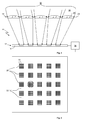
- FIG. 1 an inventive image sensor 10 is shown, which has a light receiver 12 and a light receiving optical system 14.
- the light receiver 12, the in Fig. 2 is shown in plan view, comprises a substrate 16 on which a plurality, that is typically an array, of photodiodes 18 is arranged.
- the photodiodes 18 are grouped on the substrate 16 in subarrays 20, for example each 20 x 20 or 40 x 40 photodiodes.
- the light-receiving optical system 14 is designed as a microlens array 24.
- Each microlens 26 of the microlens array 24 images part 30 of the total field of view 32 onto one subarray 20, so that overall the total field of view 32 of the image sensor 10 is imaged onto the light receiver 12.
- the reference numeral 34 is shown such an image of the light of a part of the visual field on one of the subarrays 20.
- gaps 22 are left.
- electronic components with reference to Fig. 3 will be explained in more detail below, arranged. These components serve to process the signals of the photodiodes 18 close to the pixel.
- Fig. 1 and 2 indicate light is mapped to a subarray 20, so that from the signals of the photodiodes 18 of each subarray 20, a partial image can be generated.
- a partial image is preferably created in an evaluation unit 36. From the individual partial images, an overall image of the visual field is likewise assembled in the evaluation unit 36.
- the photocurrents or photovoltage generated by the incident light 40 in the photodiodes 18 must be read out. This will be explained below on the basis of 3 and 4 explained.
- the already mentioned electronic components for pixel-near signal processing are arranged on the substrate 16 in the gaps 22.
- these components comprise, per photodiode 18, a comparator 42, a switch 44, a reference voltage source 46, a counter 48 and a clock 50.
- One terminal of the photodiode 18 is applied on the one hand via the switch 44 at a potential U 0 and on the other hand to an input 52 of the comparator 42.
- At the other comparator 54 is generated by the reference voltage source 46 reference voltage U ref .
- the output of the comparator 42 is located at the input 56 of the counter 48.
- the counter 48 receives its clock from the clock 50. Via a reset input 58, the counter 48 can be reset.
- the switch 44 When starting an image recording at the time t 0 , the switch 44 is opened and at the same time the counter 48 is released.
- the counter 48 starts with a defined counter reading, which can be generated, for example, by means of a reset operation via the reset input 58. Also conceivable is the start of a previously loaded into the counter count, which differs from the zero meter defined.
- the full voltage U 0 is applied to the comparator.
- the voltage U (t) drops. If the incidence of light is large, there is a faster decrease according to the course 60 and an earlier reaching of the reference voltage U Ref at t 1 . At lower incidence of light, the voltage U (t) decreases more slowly, which is indicated by the curve 62. The reference voltage U Ref is reached later at t 2 .
- the comparator 42 switches over, which triggers a stop of the counter 48 and / or a transfer of the counter reading to a latch. Then the count for each photodiode is a measure of the light incident on the photodiode. The meter reading is recorded in subsequent electronics for further evaluation.
- each photodiode has its own exposure time (ie each counter has its own “integration time”), namely until the photodiode voltage has fallen to U Ref .
- integration time There is no global integration time.
- the individual exposure time can only be as large as the counter depth. Is the voltage at the comparator input 52 has not yet fallen to U Ref when the maximum count is reached, it is stopped and the pixel is rated as "black”.
- an image for a subarray which corresponds to a partial image of the entire image of the visual field 32, can then be created in the evaluation unit 36. From the partial images, an overall image can subsequently be created in the evaluation unit.
- each counter 48 is always a group of n photodiodes 18 (D1 to Dn), preferably a subarray 20, assigned.
- Each photodiode 18 (D1 to Dn) with its respective associated comparator 42 (K1 to Kn) is associated with a memory 64 (M1 to Mn).
- the assignment is indicated by separate connecting lines 66.
- the respective memory 64 which is preferably designed as a latch, is used for detecting and storing the count associated with the photodiode, so that the evaluation and creation of an image can take place via the counter readings as described above.
- the synchronously started with the opening of the switches S1 to Sn for n photodiode counter 48 is clocked again by the clock unit 50.
- the output of the counter 48 applies the counter reading via a parallel or serially executed bus line 68 to the memories M1 to Mn (for n photodiodes). If the photodiode voltage at the respectively assigned comparator input 52 reaches the voltage value U Ref , the comparator switches its output (potential change). Via line 66, the counter reading of counter 48 applied to port Q is stored via enable input E of assigned memory 64.
- the entire timing of the arrangement according to the invention including opening and closing of the switch 44 and reset and / or enable input of the counter is controlled synchronously by a central clock unit.
Landscapes
- Engineering & Computer Science (AREA)
- Multimedia (AREA)
- Signal Processing (AREA)
- Transforming Light Signals Into Electric Signals (AREA)
- Facsimile Heads (AREA)
- Solid State Image Pick-Up Elements (AREA)
Priority Applications (1)
| Application Number | Priority Date | Filing Date | Title |
|---|---|---|---|
| EP13157643.1A EP2637400A3 (fr) | 2012-03-09 | 2013-03-04 | Capteur d'image et procédé de capture d'une image |
Applications Claiming Priority (2)
| Application Number | Priority Date | Filing Date | Title |
|---|---|---|---|
| EP12158802 | 2012-03-09 | ||
| EP13157643.1A EP2637400A3 (fr) | 2012-03-09 | 2013-03-04 | Capteur d'image et procédé de capture d'une image |
Publications (2)
| Publication Number | Publication Date |
|---|---|
| EP2637400A2 true EP2637400A2 (fr) | 2013-09-11 |
| EP2637400A3 EP2637400A3 (fr) | 2014-06-18 |
Family
ID=47754373
Family Applications (1)
| Application Number | Title | Priority Date | Filing Date |
|---|---|---|---|
| EP13157643.1A Ceased EP2637400A3 (fr) | 2012-03-09 | 2013-03-04 | Capteur d'image et procédé de capture d'une image |
Country Status (1)
| Country | Link |
|---|---|
| EP (1) | EP2637400A3 (fr) |
Cited By (1)
| Publication number | Priority date | Publication date | Assignee | Title |
|---|---|---|---|---|
| CN114270815A (zh) * | 2019-06-06 | 2022-04-01 | 弗劳恩霍夫应用研究促进协会 | 多通道成像设备和具有多孔径成像设备的设备 |
Families Citing this family (1)
| Publication number | Priority date | Publication date | Assignee | Title |
|---|---|---|---|---|
| US10270947B2 (en) * | 2016-09-15 | 2019-04-23 | Microsoft Technology Licensing, Llc | Flat digital image sensor |
Citations (4)
| Publication number | Priority date | Publication date | Assignee | Title |
|---|---|---|---|---|
| EP0840502A2 (fr) * | 1996-11-04 | 1998-05-06 | Eastman Kodak Company | Caméra digitale compacte avec champs de vue segmentés |
| EP0631680B1 (fr) | 1992-03-10 | 2000-06-28 | Ivp Integrated Vision Products Ab | Procede et dispositif permettant d'effectuer des operations de traitement sur des images bidimensionnelles |
| EP1646249A1 (fr) * | 2004-10-08 | 2006-04-12 | Dialog Semiconductor GmbH | Système de prise d'images stéréoscopiques avec une paire de capteurs sur une seule puce |
| US20090058993A1 (en) * | 2006-03-09 | 2009-03-05 | Siliconfile Technologies Inc. | Cmos stereo camera for obtaining three-dimensional image |
Family Cites Families (7)
| Publication number | Priority date | Publication date | Assignee | Title |
|---|---|---|---|---|
| JP2953297B2 (ja) * | 1994-03-30 | 1999-09-27 | 日本電気株式会社 | 受光素子およびその駆動方法 |
| US6330030B1 (en) * | 1998-01-05 | 2001-12-11 | Intel Corporation | Digital image sensor with low device count per pixel analog-to-digital conversion |
| US6580454B1 (en) * | 1998-11-18 | 2003-06-17 | Agilent Technologies, Inc. | CMOS active pixel sensor having in-pixel local exposure control |
| US20030206236A1 (en) * | 2002-05-06 | 2003-11-06 | Agfa Corporation | CMOS digital image sensor system and method |
| JP4071793B2 (ja) * | 2003-10-22 | 2008-04-02 | 松下電器産業株式会社 | 撮像装置とその製造方法、及び携帯機器 |
| JP5172584B2 (ja) * | 2008-10-07 | 2013-03-27 | 株式会社東芝 | 撮像装置 |
| US20100103300A1 (en) * | 2008-10-24 | 2010-04-29 | Tenebraex Corporation | Systems and methods for high resolution imaging |
-
2013
- 2013-03-04 EP EP13157643.1A patent/EP2637400A3/fr not_active Ceased
Patent Citations (4)
| Publication number | Priority date | Publication date | Assignee | Title |
|---|---|---|---|---|
| EP0631680B1 (fr) | 1992-03-10 | 2000-06-28 | Ivp Integrated Vision Products Ab | Procede et dispositif permettant d'effectuer des operations de traitement sur des images bidimensionnelles |
| EP0840502A2 (fr) * | 1996-11-04 | 1998-05-06 | Eastman Kodak Company | Caméra digitale compacte avec champs de vue segmentés |
| EP1646249A1 (fr) * | 2004-10-08 | 2006-04-12 | Dialog Semiconductor GmbH | Système de prise d'images stéréoscopiques avec une paire de capteurs sur une seule puce |
| US20090058993A1 (en) * | 2006-03-09 | 2009-03-05 | Siliconfile Technologies Inc. | Cmos stereo camera for obtaining three-dimensional image |
Non-Patent Citations (1)
| Title |
|---|
| "Belich- tungsregelung individueller Pixel von CMOS-Bildsensoren", PHOTONIC, April 2007 (2007-04-01), pages 80 |
Cited By (1)
| Publication number | Priority date | Publication date | Assignee | Title |
|---|---|---|---|---|
| CN114270815A (zh) * | 2019-06-06 | 2022-04-01 | 弗劳恩霍夫应用研究促进协会 | 多通道成像设备和具有多孔径成像设备的设备 |
Also Published As
| Publication number | Publication date |
|---|---|
| EP2637400A3 (fr) | 2014-06-18 |
Similar Documents
| Publication | Publication Date | Title |
|---|---|---|
| DE60030802T2 (de) | Bildsensor mit Messsung der Sättigungszeitmessung zur Erweiterung des Dynamikbereichs | |
| DE69827529T2 (de) | Entfernungsmessung mittels kamera | |
| AT505513B1 (de) | Bildsensor, verfahren zum betreiben eines bildsensors und computerprogramm | |
| DE69729648T2 (de) | Aktivpixelsensormatrix mit mehrfachauflösungsausgabe | |
| EP0878091B1 (fr) | Capteur d'image couleur pour exposition de courte duree | |
| DE112018005773B4 (de) | Intensitätsnormierte bildsensoren | |
| EP2040458B1 (fr) | Capteur d'images | |
| DE69821442T2 (de) | Schaltungsanordnung zur Erkennung leckender Zugriffsschalter in CMOS-Bildaufnehmerpixels | |
| DE202016105510U1 (de) | Pixel mit Global Shutter und hohem Dynamikumfang | |
| DE102016102111A1 (de) | Bildsensor und bildgebende Vorrichtung mit demselben | |
| DE69816320T2 (de) | Profilmessung mit hoher Geschwindigkeit durch CCD, das Profillinien per Bildperiode aufgreift | |
| DE102010035811B4 (de) | Bildsensor und Verfahren zum Auslesen eines Bildsensors | |
| EP2210073B1 (fr) | Circuiterie pour la production de signaux dépendant de la luminosité et de la température, notamment pour un pyromètre produisant des images | |
| DE102013208802A1 (de) | Lichtlaufzeitsensor mit spektralen Filtern | |
| WO2007031102A1 (fr) | Detection d'un rayonnement optique | |
| DE102011053219A1 (de) | Kombiniertes Pixel mit phasensensitivem und farbselektivem Subpixel | |
| DE102010028746B4 (de) | Bildsensor und Verfahren zum Aufnehmen eines Bildes | |
| DE102013208804B4 (de) | Lichtlaufzeitsensor mit zuschaltbarer Hintergrundlichtunterdrückung | |
| EP2637400A2 (fr) | Capteur d'image et procédé de capture d'une image | |
| DE102011081405B4 (de) | Bildsensor, Abbildungsvorrichtung und Verfahren für einen Bildsensor | |
| EP2870433A1 (fr) | Capteur de position optique présentant une mémoire analogique | |
| DE69817901T2 (de) | Bildsensor mit integrierter Signaldigitalisierung für Bewegungserfassung | |
| WO2000052759A1 (fr) | Dispositif capteur d'images | |
| DE10125307A1 (de) | Optischer Sensor | |
| DE112019004441T5 (de) | Bilderfassungsvorrichtung und bilderfassungselement |
Legal Events
| Date | Code | Title | Description |
|---|---|---|---|
| PUAI | Public reference made under article 153(3) epc to a published international application that has entered the european phase |
Free format text: ORIGINAL CODE: 0009012 |
|
| AK | Designated contracting states |
Kind code of ref document: A2 Designated state(s): AL AT BE BG CH CY CZ DE DK EE ES FI FR GB GR HR HU IE IS IT LI LT LU LV MC MK MT NL NO PL PT RO RS SE SI SK SM TR |
|
| AX | Request for extension of the european patent |
Extension state: BA ME |
|
| PUAL | Search report despatched |
Free format text: ORIGINAL CODE: 0009013 |
|
| AK | Designated contracting states |
Kind code of ref document: A3 Designated state(s): AL AT BE BG CH CY CZ DE DK EE ES FI FR GB GR HR HU IE IS IT LI LT LU LV MC MK MT NL NO PL PT RO RS SE SI SK SM TR |
|
| AX | Request for extension of the european patent |
Extension state: BA ME |
|
| RIC1 | Information provided on ipc code assigned before grant |
Ipc: H01L 27/144 20060101ALI20140512BHEP Ipc: H04N 5/378 20110101ALI20140512BHEP Ipc: H01L 27/146 20060101ALI20140512BHEP Ipc: H04N 5/225 20060101ALI20140512BHEP Ipc: H04N 13/02 20060101ALI20140512BHEP Ipc: H04N 5/369 20110101ALI20140512BHEP Ipc: H04N 3/14 20060101ALI20140512BHEP Ipc: H04N 5/3745 20110101AFI20140512BHEP |
|
| 17P | Request for examination filed |
Effective date: 20141127 |
|
| RBV | Designated contracting states (corrected) |
Designated state(s): AL AT BE BG CH CY CZ DE DK EE ES FI FR GB GR HR HU IE IS IT LI LT LU LV MC MK MT NL NO PL PT RO RS SE SI SK SM TR |
|
| 17Q | First examination report despatched |
Effective date: 20150409 |
|
| STAA | Information on the status of an ep patent application or granted ep patent |
Free format text: STATUS: THE APPLICATION HAS BEEN REFUSED |
|
| 18R | Application refused |
Effective date: 20160307 |