EP2642422A2 - Carte à circuit intégré et procédé de commande de carte à circuit intégré - Google Patents
Carte à circuit intégré et procédé de commande de carte à circuit intégré Download PDFInfo
- Publication number
- EP2642422A2 EP2642422A2 EP13158932.7A EP13158932A EP2642422A2 EP 2642422 A2 EP2642422 A2 EP 2642422A2 EP 13158932 A EP13158932 A EP 13158932A EP 2642422 A2 EP2642422 A2 EP 2642422A2
- Authority
- EP
- European Patent Office
- Prior art keywords
- folder
- inheritance
- card
- security status
- security
- Prior art date
- Legal status (The legal status is an assumption and is not a legal conclusion. Google has not performed a legal analysis and makes no representation as to the accuracy of the status listed.)
- Granted
Links
Images


Classifications
-
- G—PHYSICS
- G06—COMPUTING OR CALCULATING; COUNTING
- G06F—ELECTRIC DIGITAL DATA PROCESSING
- G06F21/00—Security arrangements for protecting computers, components thereof, programs or data against unauthorised activity
- G06F21/60—Protecting data
-
- G—PHYSICS
- G06—COMPUTING OR CALCULATING; COUNTING
- G06F—ELECTRIC DIGITAL DATA PROCESSING
- G06F21/00—Security arrangements for protecting computers, components thereof, programs or data against unauthorised activity
- G06F21/60—Protecting data
- G06F21/62—Protecting access to data via a platform, e.g. using keys or access control rules
- G06F21/6218—Protecting access to data via a platform, e.g. using keys or access control rules to a system of files or objects, e.g. local or distributed file system or database
-
- G—PHYSICS
- G06—COMPUTING OR CALCULATING; COUNTING
- G06F—ELECTRIC DIGITAL DATA PROCESSING
- G06F21/00—Security arrangements for protecting computers, components thereof, programs or data against unauthorised activity
- G06F21/70—Protecting specific internal or peripheral components, in which the protection of a component leads to protection of the entire computer
- G06F21/78—Protecting specific internal or peripheral components, in which the protection of a component leads to protection of the entire computer to assure secure storage of data
- G06F21/79—Protecting specific internal or peripheral components, in which the protection of a component leads to protection of the entire computer to assure secure storage of data in semiconductor storage media, e.g. directly-addressable memories
-
- G—PHYSICS
- G06—COMPUTING OR CALCULATING; COUNTING
- G06F—ELECTRIC DIGITAL DATA PROCESSING
- G06F2221/00—Indexing scheme relating to security arrangements for protecting computers, components thereof, programs or data against unauthorised activity
- G06F2221/21—Indexing scheme relating to G06F21/00 and subgroups addressing additional information or applications relating to security arrangements for protecting computers, components thereof, programs or data against unauthorised activity
- G06F2221/2145—Inheriting rights or properties, e.g., propagation of permissions or restrictions within a hierarchy
Definitions
- Embodiments described herein relate generally to an IC card, a portable electronic apparatus, and an IC card control method.
- An IC card manages a plurality of files saved in a memory by using a hierarchical structure.
- An IC card accesses each file in accordance with an established security status.
- the established security status can be inherited to each file in a lower layer belonging to the file in the upper layer.
- a security status established for a given file cannot be inherited to files in a layer higher than that of the given file or to files in the same layer as that of the given layer.
- an IC card includes a communication unit, data memory, selector, and inheriting unit.
- the communication unit performs data communication with an external apparatus.
- the data memory stores files managed by a hierarchical structure, a folder as an upper layer of the files, and information concerning the inheritance of a security status between a plurality of folders. If the communication unit receives a command requesting the selection of a second folder while a first folder is selected, the selector sets the first folder in an unselected state, and sets the second folder designated by the command in a selected state. If information indicating the inheritance of a security status from the first folder to the second folder exists, the inheriting unit inherits, even while the second file is selected, the security status established while the first folder is selected.
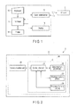
- FIG. 1 is a schematic block diagram showing an IC card (portable electronic apparatus) 2 according to the embodiment, and a configuration example of an IC card processor 1 as an external apparatus having a function of communicating with the IC card 2.
- the IC card processor 1 includes a terminal device 11, card reader/writer 12, keyboard 13, display 14, and printer 15.
- the terminal device 11 controls the operation of the whole IC card processor 1.
- the terminal device 11 includes a CPU, various memories, and various interfaces.
- the terminal device 11 is a personal computer (PC).
- the terminal device 11 has, e.g., a function of transmitting commands to the IC card 2 by the card reader/writer 12, and a function of performing various processes based on data received from the IC card 2. For example, the terminal device 11 performs control of writing data in an internal nonvolatile memory of the IC card 2 by transmitting a data write command to the IC card 2 via the card reader/writer 12. Also, the terminal device 11 performs control of reading out data from the IC card 2 by transmitting a read command to the IC card 2.
- the card reader/writer 12 is an interface device for communicating with the IC card 2.
- the card reader/writer 12 is formed by an interface corresponding to the communication system of the IC card 2.
- the card reader/writer 12 is formed by, e.g., a contact portion for physically and electrically connecting to a contact portion of the IC card 2.
- the card reader/writer 12 is formed by, e.g., an antenna and communication controller for wirelessly communicating with the IC card 2.
- the card reader/writer 12 performs power supply, clock supply, reset control, and data exchange for the IC card 2.
- the card reader/writer 12 having these functions activates (starts) the IC card 2, transmits various commands, and receives responses to the transmitted commands, under the control of the terminal device 11.
- the keyboard 13 functions as an operation unit to be operated by the operator of the IC card processor 1, and the operator inputs various operation instructions and data on the keyboard 13.
- the display 14 is a display device for displaying various kinds of information under the control of the terminal device 11.
- the printer 15 prints out various kinds of data such as processing results.
- the IC card 2 is also called a smart card.
- the IC card 2 is activated (set in an operable state) by receiving power supply from a host apparatus such as the IC card processor 1.
- a host apparatus such as the IC card processor 1.
- the IC card 2 is connected to the IC card processor 1 by contact-type communication, i.e., when the IC card 2 is a contact-type IC card, the IC card 2 is activated by receiving the supply of operation power and operation clocks from the IC card processor 1 via the contact portion as a communication interface.
- the IC card 2 when the IC card 2 is connected to the IC card processor 1 by noncontact-type communication, i.e., when the IC card 2 is a noncontact-type IC card, the IC card 2 receives a radio wave from the IC card processor 1 via, e.g., an antenna and modulator/demodulator as communication interfaces, and activates itself by generating operation power and operation clocks by a power supply unit (not shown) from the radio wave.
- a radio wave from the IC card processor 1 via, e.g., an antenna and modulator/demodulator as communication interfaces, and activates itself by generating operation power and operation clocks by a power supply unit (not shown) from the radio wave.
- FIG. 2 is a schematic block diagram showing a hardware configuration example of the IC card 2 according to the embodiment.
- the IC card 2 is obtained by incorporating a module M in a card-like housing (main body) B formed by plastic or the like.
- the module M is integrally formed in a state in which one or a plurality of IC chips C and an external interface (communication interface) for communication are connected, and embedded in the main body B.
- the module M of the IC card 2 includes a control element 21, data memory 22, working memory 23, program memory 24, and communication unit 25.
- the control element 21 controls the whole IC card 2.
- the control element 21 implements various functions by operating based on control programs and control data stored in the program memory 24 or data memory 22.
- the control element 21 controls the basic operation of the IC card 2 by executing the program of the operating system.
- the control element 21 controls various operations corresponding to the operation forms of the IC card 2 by executing application programs corresponding to the use purposes of the IC card 2.
- the data memory 22 is a nonvolatile memory such as an EEPROM (Electrically Erasable Programmable Read-Only Memory) or flash ROM in which data can be written and rewritten. Control programs or various kinds of data corresponding to the operation purposes of the IC card 2 are written in the data memory 22. Various files corresponding to the standards of the IC card 2 are defined in the data memory 22, and various kinds of data are written in these files. Examples of the files stored in the data memory 22 will be described later.
- EEPROM Electrically Erasable Programmable Read-Only Memory
- the working memory 23 is a volatile memory such as a RAM.
- the working memory (RAM) 23 also functions as a buffer for temporarily saving, e.g., data being processed by the control element 21.
- Various tables indicating, e.g., the status of access to each file, the status of use of a communication channel, and the status of processing are formed in the working memory 23. Examples of the tables formed in the working memory 23 will be described later.
- the program memory 24 is a nonvolatile memory such as a mask ROM in which control programs, control data, and the like are prestored.
- the program memory (ROM) 24 in which the control programs or control data are stored is incorporated into the IC card 2 when it is manufactured. That is, the control programs or control data stored in the program memory 24 control the basic operation of the IC card 2 and are preinstalled in accordance with the specifications of the IC card 2.
- the communication unit 25 is an interface for communicating with the card reader/writer 12 of the IC card processor 1.
- the communication unit 25 is formed by a communication controller and contact portion for exchanging signals with the card reader/writer 12 of the IC card processor 1 by physically and electrically contacting the card reader/writer 12.
- the communication unit 25 is formed by a communication controller such as a modulator/demodulator for wirelessly communicating with the card reader/writer 12 of the IC card processor 1, and an antenna for exchanging radio waves with the card reader/writer 12.
- the files stored in the data memory 22 of the IC card are managed by a hierarchical structure.
- each file stored in the data memory 22 is defined as one of an MF (Master File), DF (Dedicated File), and EF (Elementary File).
- An MF is equivalent to a root directory.
- a DF (folder) and EF (data file) are defined as layers below an MF.
- a DF is equivalent to a directory and functions as a folder.
- a DF can have a DF and EF as lower layers.
- the IC card can manage files by the hierarchical structure having an MF as the uppermost layer.
- An MF, DF, and EF are selectively used.
- FIG. 3 is a view showing examples of files managed by the hierarchical structure.
- FIG. 3 shows the management form of a hierarchical structure for files MF 301, DF (DF(A)) 302, EF (EF(A)) 304, DF (DF(B)) 305, EF (EF(B)) 307, DF (DF(C)) 308, and EF (EF(C)) 310.
- the DF(A) 302, DF(B) 305, and DF(C) 308 exist in a layer below the master file (MF) 301 in the uppermost layer.
- the EF(A) 304 exists below the DF(A) 302
- the EF(B) 307 exists below the DF(B) 305
- the EF(C) 310 exists below the DF(C) 308.
- data for implementing one application of the IC card 2 is stored in each DF.
- a plurality of DFs corresponding to the applications can be formed in the data memory 22.
- the DFs 302, 305, and 308 respectively have FCIs (File Control Information) 303, 306, and 309.
- the FCIs 303, 306, and 309 are control information pertaining to the respective corresponding DFs 302, 305, and 308.
- information such as the security condition of a corresponding EF is stored in each of the FCIs 303, 306, and 309.
- the FCI can also be defined by the ISO/IEC 7816-4 as one standard of an IC card.
- command data (to be simply referred to as a command hereinafter) to be supplied to the IC card 2 will be explained.
- FIG. 4 shows a configuration example of a select command for requesting file selection.
- FIG. 4 shows a configuration example of a select command defined by the ISO/IEC 7816-3.
- the select command shown in FIG. 4 complies with the Command Application Protocol Data Unit format defined by the ISO/IEC 7816-3.
- the command includes a "Class byte (CLA)" field 401, "Instruction byte (INS)” field 402, "P1” field 403, “P2” field 404, "Lc” field 405, "Data” field 406, and "Le” field 407.
- the CLA field 401 and INS field 402 store information indicating the type of command.
- the P1 field 403 and P2 field 404 store parameters for command processing.
- the Lc field 405 stores information indicating the length of the Data field 406.
- the Data field 406 stores data to be used in the command.
- the Le field 407 stores information for checking the command.
- the Data field 406 of the select command stores a file name as a selection target.
- "A0 00 01" is stored as a DF name in the "Data" field.
- response data (to be also simply referred to as a response hereinafter) with respect to a command will be explained below.
- FIG. 5 is a view showing a configuration example of the response to the select command.
- the response includes a data field and status field.
- the data field of the response stores data indicating, e.g., the execution result of the command
- the status field of the response stores a status indicating the success or failure of processing corresponding to the command.
- the data field of the response is object data having a TLV structure in which an identifier (Tag) 501, length information (Length) 502, and data field (Value) 503 are connected in this order.
- the data field (the value of parent data) 503 shown in FIG. 5 stores data (child data) containing a tag 511, length 512, and value 513.
- the value 513 of the child data shown in FIG. 5 stores first data (first grandchild data) containing a tag 521, length 522, and value 523, and second data (second grandchild data) containing a tag 531, length 532, and value 533.
- the data configuration indicated by 501 to 533 is the configuration of a constructed data object defined by the ISO/IEC 7816-4.
- FIG. 5 shows a practical example of the response to the select command.
- the data fields 501 to 533 shown in FIG. 5 form the FCI of a file selected by the select command. That is, in the example shown in FIG. 5 , the tag 501 is the identifier of the FCI of the selected file, the length 502 indicates the whole length of the FCI of the selected file, and the value 503 is real data in the FCI of the selected file. In the example shown in FIG. 5 , the value 503 contains data indicating the inheritance of the security condition of the selected file.
- the data (first grandchild data) indicated by the tag 521 is TLV data storing information indicating a file as the inheritance source or inheritance destination of the security condition of the selected file.
- the tag 521 is the identifier of the first grandchild data.
- the length 522 is information indicating the length of the succeeding value 523.
- the value 523 is information (the tag of a DF name) indicating the file as the inheritance source or inheritance destination of the security condition.
- the data (second grandchild data) indicated by the tag 531 includes the TLV data 531, 532, and 533 storing data indicating the inheriting condition of the security condition.
- the tag 531 is the identifier of the second grandchild data.
- the length 532 is information indicating the length of the succeeding value 533.
- the value 533 is information indicating "the inheriting condition of the security condition" for identifying whether to inherit the security condition when verify is performed, inherit the security condition when authentication is performed, or inherit the session key and condition of secure messaging, when inheriting the security condition.
- the value 533 can be 1-byte data
- bit 8 can indicate authentication
- bit 7 can indicate verify
- bit 6 can indicate the inheritance of the session key for secure messaging.
- FIG. 6 is a view showing an example of information stored in the working memory 23 after the select command is executed.
- FIG. 6 shows examples of information indicating the selected state and security status of a DF to be stored in the RAM of the IC card according to the embodiment.
- data 602 to 608 are stored as the execution results of the select command in the working memory (RAM) 23.
- the data 602 stores information (the file name of a file presently being selected (the DF name of a DF)) indicating a file to be selected by the select command.
- This information stored in the data 602 is information (DF identification information containing the DF name) indicating the file selected by the select command.
- the data 603 stores information indicating the security condition (security status) such as an authority established by verify with an external apparatus (IC card processor).
- the data 604 stores information indicating the security condition (security status) such as an authority established by authentication with an external apparatus.
- the data 605 stores information indicating a session key (key information) to be used in secure messaging.
- the data 606 stores a status (secure messaging execution condition) indicating whether secure messaging can be performed.
- the data 607 stores information (DF identification information containing the DF name) indicating a DF (folder) set in the selected state before the selecting process is performed by the select command.
- the data 608 stores FCI of the DF (folder) set in the selected state before the selecting process is performed by the select command.
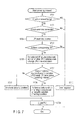
- FIG. 7 is a flowchart for explaining the procedure of the selecting process for the select command in the IC card 2.
- control element 21 When receiving a command from the IC card processor 1, the control element 21 checks the format of the received command (step S702). If the control element 21 determines that the format of the received command is abnormal (NG in step S702), the control element 21 outputs, as an error response, a response indicating that the format of the command is abnormal (step S710), and terminates the process.
- control element 21 determines that the format of the received command is normal (OK in step S702)
- the control element 21 checks the command parameters (step S703), and discriminates the process contents of the received command. For example, the control element 21 of the IC card 2 discriminates the type of the received command by "CLA” and "INS" of the received command, and discriminates the process contents by "P1", "P2", and "Data”. If the control element 21 determines that the parameters of the received command are abnormal (NG in step S703), the control element 21 outputs, as an error response, a response indicating that the parameters of the command are abnormal (step S710), and terminates the process.
- the control element 21 of the IC card 2 has received a select command requesting the selection of a given DF from the IC card processor 1 by the communication unit 25. If the control element 21 of the IC card 2 has received a select command having normal parameters (OK in step S703), the control element 21 recognizes that the received command is a select command by "CLA” and "INS" of the received command, and starts a selecting process of setting the DF designated by "P1", "P2", and "Data" in the selected state.
- the control element 21 performs a process of searching for the DF designated by the select command (step S704). If the control element 21 determines that the designated DF does not exist in the data memory 22 (NO in step S705), the control element 21 outputs, as an error response, a response indicating that the file designated by the command does not exist (step S710), and terminates the process.
- step S705 the control element 21 performs a process of changing DFs in the selected state, as the process of setting the designated DF in the selected state (step S706). That is, the control element 21 updates a DF in the selected state as shown in FIG. 6 , thereby setting a DF presently being selected in the unselected state, and setting the DF designated by the command in the selected state.
- This DF changing process is implemented by, e.g., updating the information on the RAM 23 as shown in FIG. 6 .
- the control element 21 updates the identification information of a DF to be set in the selected state to the identification information of the DF designated by the select command in the data 602 indicating a DF in the selected state in the RAM 23, thereby setting the DF designated by the command in the selected state.
- the control element 21 writes the identification information of a DF in the selected state in the data 607 indicating a DF set in the selected state before the selecting process, thereby setting the DF presently being selected in the unselected state.
- the control element 21 writes the FCI of the DF set in the selected state before the selecting process in the data 608.
- the control element 21 determines whether the inheritance of the security status is possible even after the DFs in the selected state are changed (step S707).
- information indicating a DF as the inheritance source of the security condition (security status) is stored in the FCI of each DF. It is also possible to set, in the FCI of each DF, a plurality of pieces of information (e.g., DF names) each indicating a DF as the inheritance source of the security condition (security status).
- the control element 21 determines, by the FCI of the DF set in the selected state, whether it is possible to inherit the security status established while a DF set in the selected state before the selecting process is selected (step S707).
- the control element 21 checks whether information indicating the DF as the security condition inheritance source stored in the FCI of the DF set in the selected state matches the DF set in the selected state before the selecting process.
- the control element 21 performs a security condition inheriting process based on the security condition (security status) inheriting condition stored in the FCI of the DF set in the selected state (step S708).
- the control element 21 sets the FCI of the DF set in the selected state in the data field as a response to the received select command, and sets a status indicating normal termination in the status field (SW1 and SW2), thereby forming response data as a response to the received select command.
- the control element 21 outputs the formed response data to the IC card processor 1 (step S709), and terminates the process.
- the control element 21 invalidates the security condition (security status) established before the selecting process (e.g., clears the data 603 to 606 in the RAM 23) (step S712).
- the control element 21 sets the FCI of the DF set in the selected state in the data field, and sets a status indicating normal termination in the status field (SW1 and SW2), thereby forming response data as a response to the received select command.
- the control element 21 outputs the formed response data to the IC card processor 1 (step S709), and terminates the process.
- FIG. 8 is a flowchart for explaining the procedure of the selecting process for the select command in the IC card 2.
- control element 21 When receiving a command from the IC card processor 1, the control element 21 checks the format of the received command (step S802). If the control element 21 determines that the format of the received command is abnormal (NG in step S802), the control element 21 outputs, as an error response, a response indicating that the format of the command is abnormal (step S810), and terminates the process.
- control element 21 determines that the format of the received command is normal (OK in step S802)
- the control element 21 checks the command parameters (step S803), and discriminates the process contents of the received command. For example, the control element 21 of the IC card 2 discriminates the type of the received command by "CLA” and "INS" of the received command, and discriminates the process contents by "P1", "P2", and "Data”. If the control element 21 determines that the parameters of the received command are abnormal (NG in step S803), the control element 21 outputs, as an error response, a response indicating that the parameters of the command are abnormal (step S810), and terminates the process.
- the control element 21 of the IC card 2 has received a select command requesting the selection of a given DF from the IC card processor 1 by the communication unit 25. If the control element 21 of the IC card 2 has received a select command having normal parameters (OK in step S803), the control element 21 recognizes that the received command is a select command by "CLA” and "INS" of the received command, and starts a selecting process of setting the DF designated by "P1", "P2", and "Data" in the selected state.
- the control element 21 performs a process of searching for the DF designated by the select command (step S804). If the control element 21 determines that the designated DF does not exist in the data memory 22 (NO in step S805), the control element 21 outputs, as an error response, a response indicating that the file designated by the command does not exist (step S810), and terminates the process.
- step S805 the control element 21 performs a process of changing DFs in the selected state, as the process of setting the designated DF in the selected state (step S806). That is, the control element 21 updates a DF in the selected state as shown in FIG. 6 , thereby setting a DF presently being selected in the unselected state, and setting the DF designated by the command in the selected state.
- the control element 21 determines whether the inheritance of the security status is possible even after the DFs in the selected state are changed (step S807).
- information indicating a DF as the inheritance destination of the security condition (security status) is stored in the FCI of each DF. It is also possible to set, in the FCI of each DF, a plurality of pieces of information (e.g., DF names) each indicating a DF as the inheritance destination of the security condition (security status).
- the control element 21 determines, by the FCI of the DF set in the selected state before the selecting process, whether it is possible to inherit the security status established while a DF set in the selected state before the selecting process is selected (step S807), even after the DFs in the selected state are changed.
- the control element 21 checks whether information indicating the DF as the security condition inheritance destination stored in the FCI of the DF set in the selected state before the selecting process matches the DF set in the selected state.
- the control element 21 performs a security condition inheriting process based on the security condition (security status) inheriting condition stored in the FCI of the DF set in the selected state (step S808).
- the control element 21 sets the FCI of the DF set in the selected state in the data field as a response to the received select command, and sets a status indicating normal termination in the status field (SW1 and SW2), thereby forming response data as a response to the received select command.
- the control element 21 outputs the formed response data to the IC card processor 1 (step S809), and terminates the process.
- the control element 21 invalidates the security condition (security status) established before the selecting process (e.g., clears the data 603 to 606 in the RAM 23) (step S812).
- the control element 21 sets the FCI of the DF set in the selected state in the data field, and sets a status indicating normal termination in the status field (SW1 and SW2), thereby forming response data as a response to the received select command.
- the control element 21 outputs the formed response data to the IC card processor 1 (step S809), and terminates the process.
- the information concerning the inheritance of the security status is set in the FCI as control information for a DF.
- a DF or a plurality of DFs
- a DF or a plurality of DFs
- the inheritance destination of the security status is designated. Consequently, DFs in, e.g., the same layer of the IC card can share the security status, and the security status can be inherited even when a select command is executed.
- the inheriting condition can be set for the inheritance of the security status.
- the inheriting condition of the security status can be set in the FCI of a DF.
- the security condition (security status) as a target of inheritance are whether secure messaging can be performed, an authority obtained by the success of verify with an external apparatus, an authority obtained by the success of authentication with an external apparatus, the key for use in secure messaging, and the executing condition of secure messaging.
Landscapes
- Engineering & Computer Science (AREA)
- Theoretical Computer Science (AREA)
- Computer Hardware Design (AREA)
- Computer Security & Cryptography (AREA)
- General Engineering & Computer Science (AREA)
- Software Systems (AREA)
- Physics & Mathematics (AREA)
- General Physics & Mathematics (AREA)
- General Health & Medical Sciences (AREA)
- Bioethics (AREA)
- Health & Medical Sciences (AREA)
- Databases & Information Systems (AREA)
- Storage Device Security (AREA)
- Information Retrieval, Db Structures And Fs Structures Therefor (AREA)
Applications Claiming Priority (1)
| Application Number | Priority Date | Filing Date | Title |
|---|---|---|---|
| JP2012063365A JP5843674B2 (ja) | 2012-03-21 | 2012-03-21 | Icカード、携帯可能電子装置及びicカードの制御方法 |
Publications (3)
| Publication Number | Publication Date |
|---|---|
| EP2642422A2 true EP2642422A2 (fr) | 2013-09-25 |
| EP2642422A3 EP2642422A3 (fr) | 2016-10-26 |
| EP2642422B1 EP2642422B1 (fr) | 2018-04-25 |
Family
ID=48044535
Family Applications (1)
| Application Number | Title | Priority Date | Filing Date |
|---|---|---|---|
| EP13158932.7A Active EP2642422B1 (fr) | 2012-03-21 | 2013-03-13 | Carte à circuit intégré et procédé de commande de carte à circuit intégré |
Country Status (3)
| Country | Link |
|---|---|
| US (1) | US9183400B2 (fr) |
| EP (1) | EP2642422B1 (fr) |
| JP (1) | JP5843674B2 (fr) |
Families Citing this family (9)
| Publication number | Priority date | Publication date | Assignee | Title |
|---|---|---|---|---|
| JP6833364B2 (ja) * | 2016-07-01 | 2021-02-24 | 株式会社東芝 | Icカード、および、icカード処理装置 |
| US10496327B1 (en) | 2016-09-28 | 2019-12-03 | Amazon Technologies, Inc. | Command parallelization for data storage systems |
| US11204895B1 (en) | 2016-09-28 | 2021-12-21 | Amazon Technologies, Inc. | Data payload clustering for data storage systems |
| US10657097B1 (en) | 2016-09-28 | 2020-05-19 | Amazon Technologies, Inc. | Data payload aggregation for data storage systems |
| US10810157B1 (en) * | 2016-09-28 | 2020-10-20 | Amazon Technologies, Inc. | Command aggregation for data storage operations |
| US11281624B1 (en) | 2016-09-28 | 2022-03-22 | Amazon Technologies, Inc. | Client-based batching of data payload |
| US10437790B1 (en) | 2016-09-28 | 2019-10-08 | Amazon Technologies, Inc. | Contextual optimization for data storage systems |
| JP2018190194A (ja) * | 2017-05-08 | 2018-11-29 | 凸版印刷株式会社 | Icカード及びicカードの制御方法 |
| JP7020969B2 (ja) * | 2018-03-16 | 2022-02-16 | 株式会社東芝 | 携帯可能電子装置、及びicカード |
Family Cites Families (6)
| Publication number | Priority date | Publication date | Assignee | Title |
|---|---|---|---|---|
| JP3565481B2 (ja) * | 1998-11-19 | 2004-09-15 | 株式会社エヌ・ティ・ティ・データ | コンピュータのディレクトリアクセス制御システム及び方法 |
| JP2002312741A (ja) | 2001-04-10 | 2002-10-25 | Ntt Data Corp | Icカード及びプログラム |
| JP2005128996A (ja) * | 2003-09-30 | 2005-05-19 | Dainippon Printing Co Ltd | 情報処理装置、情報処理システム及びプログラム |
| JP4828809B2 (ja) * | 2003-12-10 | 2011-11-30 | 株式会社東芝 | Icカードおよびicカードにおける処理方法 |
| JP4891587B2 (ja) * | 2005-09-30 | 2012-03-07 | 株式会社東芝 | 携帯可能電子装置、icカードおよびicモジュール |
| JP5329884B2 (ja) * | 2008-09-18 | 2013-10-30 | 株式会社東芝 | 携帯可能電子装置および携帯可能電子装置におけるデータ処理方法 |
-
2012
- 2012-03-21 JP JP2012063365A patent/JP5843674B2/ja active Active
-
2013
- 2013-03-12 US US13/794,991 patent/US9183400B2/en active Active
- 2013-03-13 EP EP13158932.7A patent/EP2642422B1/fr active Active
Non-Patent Citations (1)
| Title |
|---|
| None |
Also Published As
| Publication number | Publication date |
|---|---|
| EP2642422B1 (fr) | 2018-04-25 |
| US9183400B2 (en) | 2015-11-10 |
| JP2013196436A (ja) | 2013-09-30 |
| US20130254904A1 (en) | 2013-09-26 |
| JP5843674B2 (ja) | 2016-01-13 |
| EP2642422A3 (fr) | 2016-10-26 |
Similar Documents
| Publication | Publication Date | Title |
|---|---|---|
| EP2642422B1 (fr) | Carte à circuit intégré et procédé de commande de carte à circuit intégré | |
| US8931705B2 (en) | IC card, mobile electronic device and data processing method in IC card | |
| US10498671B2 (en) | IC card, portable electronic apparatus, and IC card processing apparatus | |
| US20090177921A1 (en) | Portable electronic device and control method thereof | |
| JP6039036B2 (ja) | Icカード、携帯可能電子装置及びicカードの制御方法 | |
| EP3379424B1 (fr) | Carte à circuit intégré, dispositif électronique portable, programme, appareil de traitement et système de traitement | |
| JP6984328B2 (ja) | 電子情報記憶媒体、icカード、外部機器、データ書き込み方法及びデータ書き込みプログラム | |
| JP5957347B2 (ja) | Icカード、および携帯可能電子装置 | |
| JP7631895B2 (ja) | Icカード | |
| EP2642411B1 (fr) | Carte à circuit intégré et procédé de traitement de commande pour carte à circuit intégré | |
| US20090083273A1 (en) | Portable electronic apparatus and control method for portable electronic apparatus | |
| JP5932588B2 (ja) | Icカード、携帯可能電子装置、及びicカード処理装置 | |
| JP6071677B2 (ja) | Icカード、icモジュールおよび携帯可能電子装置 | |
| JP2012133656A (ja) | 携帯可能電子装置及びicカード | |
| EP3144905B1 (fr) | Carte à circuit intégré et module de circuit intégré | |
| JP2024139134A (ja) | 電子情報記憶媒体、icチップ、発行データの書き込み方法、及びプログラム | |
| JP2006293706A (ja) | アプリケーションの更新機能を有するマルチアプリケーションicカード | |
| JP2008242998A (ja) | Icカード | |
| JP2014006631A (ja) | Icカード、および、携帯可能電子装置 | |
| JP2014182639A (ja) | Icカードおよび携帯可能電子装置 | |
| JP2012155664A (ja) | 携帯可能電子装置及びicカード |
Legal Events
| Date | Code | Title | Description |
|---|---|---|---|
| PUAI | Public reference made under article 153(3) epc to a published international application that has entered the european phase |
Free format text: ORIGINAL CODE: 0009012 |
|
| 17P | Request for examination filed |
Effective date: 20130313 |
|
| AK | Designated contracting states |
Kind code of ref document: A2 Designated state(s): AL AT BE BG CH CY CZ DE DK EE ES FI FR GB GR HR HU IE IS IT LI LT LU LV MC MK MT NL NO PL PT RO RS SE SI SK SM TR |
|
| AX | Request for extension of the european patent |
Extension state: BA ME |
|
| PUAL | Search report despatched |
Free format text: ORIGINAL CODE: 0009013 |
|
| AK | Designated contracting states |
Kind code of ref document: A3 Designated state(s): AL AT BE BG CH CY CZ DE DK EE ES FI FR GB GR HR HU IE IS IT LI LT LU LV MC MK MT NL NO PL PT RO RS SE SI SK SM TR |
|
| AX | Request for extension of the european patent |
Extension state: BA ME |
|
| RIC1 | Information provided on ipc code assigned before grant |
Ipc: G06F 21/60 20130101ALI20160916BHEP Ipc: G06F 21/62 20130101ALI20160916BHEP Ipc: G06F 21/79 20130101AFI20160916BHEP |
|
| STAA | Information on the status of an ep patent application or granted ep patent |
Free format text: STATUS: EXAMINATION IS IN PROGRESS |
|
| 17Q | First examination report despatched |
Effective date: 20170620 |
|
| GRAP | Despatch of communication of intention to grant a patent |
Free format text: ORIGINAL CODE: EPIDOSNIGR1 |
|
| STAA | Information on the status of an ep patent application or granted ep patent |
Free format text: STATUS: GRANT OF PATENT IS INTENDED |
|
| INTG | Intention to grant announced |
Effective date: 20171113 |
|
| GRAS | Grant fee paid |
Free format text: ORIGINAL CODE: EPIDOSNIGR3 |
|
| GRAA | (expected) grant |
Free format text: ORIGINAL CODE: 0009210 |
|
| STAA | Information on the status of an ep patent application or granted ep patent |
Free format text: STATUS: THE PATENT HAS BEEN GRANTED |
|
| AK | Designated contracting states |
Kind code of ref document: B1 Designated state(s): AL AT BE BG CH CY CZ DE DK EE ES FI FR GB GR HR HU IE IS IT LI LT LU LV MC MK MT NL NO PL PT RO RS SE SI SK SM TR |
|
| REG | Reference to a national code |
Ref country code: GB Ref legal event code: FG4D |
|
| REG | Reference to a national code |
Ref country code: CH Ref legal event code: EP |
|
| REG | Reference to a national code |
Ref country code: AT Ref legal event code: REF Ref document number: 993648 Country of ref document: AT Kind code of ref document: T Effective date: 20180515 |
|
| REG | Reference to a national code |
Ref country code: IE Ref legal event code: FG4D |
|
| REG | Reference to a national code |
Ref country code: DE Ref legal event code: R096 Ref document number: 602013036339 Country of ref document: DE |
|
| REG | Reference to a national code |
Ref country code: NL Ref legal event code: MP Effective date: 20180425 |
|
| REG | Reference to a national code |
Ref country code: LT Ref legal event code: MG4D |
|
| PG25 | Lapsed in a contracting state [announced via postgrant information from national office to epo] |
Ref country code: NL Free format text: LAPSE BECAUSE OF FAILURE TO SUBMIT A TRANSLATION OF THE DESCRIPTION OR TO PAY THE FEE WITHIN THE PRESCRIBED TIME-LIMIT Effective date: 20180425 |
|
| PG25 | Lapsed in a contracting state [announced via postgrant information from national office to epo] |
Ref country code: PL Free format text: LAPSE BECAUSE OF FAILURE TO SUBMIT A TRANSLATION OF THE DESCRIPTION OR TO PAY THE FEE WITHIN THE PRESCRIBED TIME-LIMIT Effective date: 20180425 Ref country code: NO Free format text: LAPSE BECAUSE OF FAILURE TO SUBMIT A TRANSLATION OF THE DESCRIPTION OR TO PAY THE FEE WITHIN THE PRESCRIBED TIME-LIMIT Effective date: 20180725 Ref country code: SE Free format text: LAPSE BECAUSE OF FAILURE TO SUBMIT A TRANSLATION OF THE DESCRIPTION OR TO PAY THE FEE WITHIN THE PRESCRIBED TIME-LIMIT Effective date: 20180425 Ref country code: FI Free format text: LAPSE BECAUSE OF FAILURE TO SUBMIT A TRANSLATION OF THE DESCRIPTION OR TO PAY THE FEE WITHIN THE PRESCRIBED TIME-LIMIT Effective date: 20180425 Ref country code: BG Free format text: LAPSE BECAUSE OF FAILURE TO SUBMIT A TRANSLATION OF THE DESCRIPTION OR TO PAY THE FEE WITHIN THE PRESCRIBED TIME-LIMIT Effective date: 20180725 Ref country code: ES Free format text: LAPSE BECAUSE OF FAILURE TO SUBMIT A TRANSLATION OF THE DESCRIPTION OR TO PAY THE FEE WITHIN THE PRESCRIBED TIME-LIMIT Effective date: 20180425 Ref country code: LT Free format text: LAPSE BECAUSE OF FAILURE TO SUBMIT A TRANSLATION OF THE DESCRIPTION OR TO PAY THE FEE WITHIN THE PRESCRIBED TIME-LIMIT Effective date: 20180425 |
|
| PG25 | Lapsed in a contracting state [announced via postgrant information from national office to epo] |
Ref country code: LV Free format text: LAPSE BECAUSE OF FAILURE TO SUBMIT A TRANSLATION OF THE DESCRIPTION OR TO PAY THE FEE WITHIN THE PRESCRIBED TIME-LIMIT Effective date: 20180425 Ref country code: HR Free format text: LAPSE BECAUSE OF FAILURE TO SUBMIT A TRANSLATION OF THE DESCRIPTION OR TO PAY THE FEE WITHIN THE PRESCRIBED TIME-LIMIT Effective date: 20180425 Ref country code: GR Free format text: LAPSE BECAUSE OF FAILURE TO SUBMIT A TRANSLATION OF THE DESCRIPTION OR TO PAY THE FEE WITHIN THE PRESCRIBED TIME-LIMIT Effective date: 20180726 Ref country code: RS Free format text: LAPSE BECAUSE OF FAILURE TO SUBMIT A TRANSLATION OF THE DESCRIPTION OR TO PAY THE FEE WITHIN THE PRESCRIBED TIME-LIMIT Effective date: 20180425 |
|
| REG | Reference to a national code |
Ref country code: AT Ref legal event code: MK05 Ref document number: 993648 Country of ref document: AT Kind code of ref document: T Effective date: 20180425 |
|
| PG25 | Lapsed in a contracting state [announced via postgrant information from national office to epo] |
Ref country code: PT Free format text: LAPSE BECAUSE OF FAILURE TO SUBMIT A TRANSLATION OF THE DESCRIPTION OR TO PAY THE FEE WITHIN THE PRESCRIBED TIME-LIMIT Effective date: 20180827 |
|
| REG | Reference to a national code |
Ref country code: DE Ref legal event code: R097 Ref document number: 602013036339 Country of ref document: DE |
|
| PG25 | Lapsed in a contracting state [announced via postgrant information from national office to epo] |
Ref country code: AT Free format text: LAPSE BECAUSE OF FAILURE TO SUBMIT A TRANSLATION OF THE DESCRIPTION OR TO PAY THE FEE WITHIN THE PRESCRIBED TIME-LIMIT Effective date: 20180425 Ref country code: DK Free format text: LAPSE BECAUSE OF FAILURE TO SUBMIT A TRANSLATION OF THE DESCRIPTION OR TO PAY THE FEE WITHIN THE PRESCRIBED TIME-LIMIT Effective date: 20180425 Ref country code: EE Free format text: LAPSE BECAUSE OF FAILURE TO SUBMIT A TRANSLATION OF THE DESCRIPTION OR TO PAY THE FEE WITHIN THE PRESCRIBED TIME-LIMIT Effective date: 20180425 Ref country code: RO Free format text: LAPSE BECAUSE OF FAILURE TO SUBMIT A TRANSLATION OF THE DESCRIPTION OR TO PAY THE FEE WITHIN THE PRESCRIBED TIME-LIMIT Effective date: 20180425 Ref country code: CZ Free format text: LAPSE BECAUSE OF FAILURE TO SUBMIT A TRANSLATION OF THE DESCRIPTION OR TO PAY THE FEE WITHIN THE PRESCRIBED TIME-LIMIT Effective date: 20180425 Ref country code: SK Free format text: LAPSE BECAUSE OF FAILURE TO SUBMIT A TRANSLATION OF THE DESCRIPTION OR TO PAY THE FEE WITHIN THE PRESCRIBED TIME-LIMIT Effective date: 20180425 |
|
| PG25 | Lapsed in a contracting state [announced via postgrant information from national office to epo] |
Ref country code: SM Free format text: LAPSE BECAUSE OF FAILURE TO SUBMIT A TRANSLATION OF THE DESCRIPTION OR TO PAY THE FEE WITHIN THE PRESCRIBED TIME-LIMIT Effective date: 20180425 Ref country code: IT Free format text: LAPSE BECAUSE OF FAILURE TO SUBMIT A TRANSLATION OF THE DESCRIPTION OR TO PAY THE FEE WITHIN THE PRESCRIBED TIME-LIMIT Effective date: 20180425 |
|
| PLBE | No opposition filed within time limit |
Free format text: ORIGINAL CODE: 0009261 |
|
| STAA | Information on the status of an ep patent application or granted ep patent |
Free format text: STATUS: NO OPPOSITION FILED WITHIN TIME LIMIT |
|
| 26N | No opposition filed |
Effective date: 20190128 |
|
| PG25 | Lapsed in a contracting state [announced via postgrant information from national office to epo] |
Ref country code: SI Free format text: LAPSE BECAUSE OF FAILURE TO SUBMIT A TRANSLATION OF THE DESCRIPTION OR TO PAY THE FEE WITHIN THE PRESCRIBED TIME-LIMIT Effective date: 20180425 |
|
| PG25 | Lapsed in a contracting state [announced via postgrant information from national office to epo] |
Ref country code: MC Free format text: LAPSE BECAUSE OF FAILURE TO SUBMIT A TRANSLATION OF THE DESCRIPTION OR TO PAY THE FEE WITHIN THE PRESCRIBED TIME-LIMIT Effective date: 20180425 |
|
| REG | Reference to a national code |
Ref country code: CH Ref legal event code: PL |
|
| GBPC | Gb: european patent ceased through non-payment of renewal fee |
Effective date: 20190313 |
|
| PG25 | Lapsed in a contracting state [announced via postgrant information from national office to epo] |
Ref country code: AL Free format text: LAPSE BECAUSE OF FAILURE TO SUBMIT A TRANSLATION OF THE DESCRIPTION OR TO PAY THE FEE WITHIN THE PRESCRIBED TIME-LIMIT Effective date: 20180425 Ref country code: LU Free format text: LAPSE BECAUSE OF NON-PAYMENT OF DUE FEES Effective date: 20190313 |
|
| REG | Reference to a national code |
Ref country code: BE Ref legal event code: MM Effective date: 20190331 |
|
| PG25 | Lapsed in a contracting state [announced via postgrant information from national office to epo] |
Ref country code: LI Free format text: LAPSE BECAUSE OF NON-PAYMENT OF DUE FEES Effective date: 20190331 Ref country code: IE Free format text: LAPSE BECAUSE OF NON-PAYMENT OF DUE FEES Effective date: 20190313 Ref country code: CH Free format text: LAPSE BECAUSE OF NON-PAYMENT OF DUE FEES Effective date: 20190331 Ref country code: GB Free format text: LAPSE BECAUSE OF NON-PAYMENT OF DUE FEES Effective date: 20190313 |
|
| PG25 | Lapsed in a contracting state [announced via postgrant information from national office to epo] |
Ref country code: BE Free format text: LAPSE BECAUSE OF NON-PAYMENT OF DUE FEES Effective date: 20190331 |
|
| PG25 | Lapsed in a contracting state [announced via postgrant information from national office to epo] |
Ref country code: TR Free format text: LAPSE BECAUSE OF FAILURE TO SUBMIT A TRANSLATION OF THE DESCRIPTION OR TO PAY THE FEE WITHIN THE PRESCRIBED TIME-LIMIT Effective date: 20180425 |
|
| PG25 | Lapsed in a contracting state [announced via postgrant information from national office to epo] |
Ref country code: MT Free format text: LAPSE BECAUSE OF NON-PAYMENT OF DUE FEES Effective date: 20190313 |
|
| PG25 | Lapsed in a contracting state [announced via postgrant information from national office to epo] |
Ref country code: CY Free format text: LAPSE BECAUSE OF FAILURE TO SUBMIT A TRANSLATION OF THE DESCRIPTION OR TO PAY THE FEE WITHIN THE PRESCRIBED TIME-LIMIT Effective date: 20180425 |
|
| PG25 | Lapsed in a contracting state [announced via postgrant information from national office to epo] |
Ref country code: IS Free format text: LAPSE BECAUSE OF FAILURE TO SUBMIT A TRANSLATION OF THE DESCRIPTION OR TO PAY THE FEE WITHIN THE PRESCRIBED TIME-LIMIT Effective date: 20180825 |
|
| PG25 | Lapsed in a contracting state [announced via postgrant information from national office to epo] |
Ref country code: HU Free format text: LAPSE BECAUSE OF FAILURE TO SUBMIT A TRANSLATION OF THE DESCRIPTION OR TO PAY THE FEE WITHIN THE PRESCRIBED TIME-LIMIT; INVALID AB INITIO Effective date: 20130313 |
|
| PG25 | Lapsed in a contracting state [announced via postgrant information from national office to epo] |
Ref country code: MK Free format text: LAPSE BECAUSE OF FAILURE TO SUBMIT A TRANSLATION OF THE DESCRIPTION OR TO PAY THE FEE WITHIN THE PRESCRIBED TIME-LIMIT Effective date: 20180425 |
|
| PGFP | Annual fee paid to national office [announced via postgrant information from national office to epo] |
Ref country code: FR Payment date: 20251231 Year of fee payment: 14 |
|
| PGFP | Annual fee paid to national office [announced via postgrant information from national office to epo] |
Ref country code: DE Payment date: 20260102 Year of fee payment: 14 |