EP2642422B1 - Carte à circuit intégré et procédé de commande de carte à circuit intégré - Google Patents
Carte à circuit intégré et procédé de commande de carte à circuit intégré Download PDFInfo
- Publication number
- EP2642422B1 EP2642422B1 EP13158932.7A EP13158932A EP2642422B1 EP 2642422 B1 EP2642422 B1 EP 2642422B1 EP 13158932 A EP13158932 A EP 13158932A EP 2642422 B1 EP2642422 B1 EP 2642422B1
- Authority
- EP
- European Patent Office
- Prior art keywords
- folder
- card
- inheritance
- security status
- security
- Prior art date
- Legal status (The legal status is an assumption and is not a legal conclusion. Google has not performed a legal analysis and makes no representation as to the accuracy of the status listed.)
- Active
Links
Images


Classifications
-
- G—PHYSICS
- G06—COMPUTING OR CALCULATING; COUNTING
- G06F—ELECTRIC DIGITAL DATA PROCESSING
- G06F21/00—Security arrangements for protecting computers, components thereof, programs or data against unauthorised activity
- G06F21/60—Protecting data
-
- G—PHYSICS
- G06—COMPUTING OR CALCULATING; COUNTING
- G06F—ELECTRIC DIGITAL DATA PROCESSING
- G06F21/00—Security arrangements for protecting computers, components thereof, programs or data against unauthorised activity
- G06F21/60—Protecting data
- G06F21/62—Protecting access to data via a platform, e.g. using keys or access control rules
- G06F21/6218—Protecting access to data via a platform, e.g. using keys or access control rules to a system of files or objects, e.g. local or distributed file system or database
-
- G—PHYSICS
- G06—COMPUTING OR CALCULATING; COUNTING
- G06F—ELECTRIC DIGITAL DATA PROCESSING
- G06F21/00—Security arrangements for protecting computers, components thereof, programs or data against unauthorised activity
- G06F21/70—Protecting specific internal or peripheral components, in which the protection of a component leads to protection of the entire computer
- G06F21/78—Protecting specific internal or peripheral components, in which the protection of a component leads to protection of the entire computer to assure secure storage of data
- G06F21/79—Protecting specific internal or peripheral components, in which the protection of a component leads to protection of the entire computer to assure secure storage of data in semiconductor storage media, e.g. directly-addressable memories
-
- G—PHYSICS
- G06—COMPUTING OR CALCULATING; COUNTING
- G06F—ELECTRIC DIGITAL DATA PROCESSING
- G06F2221/00—Indexing scheme relating to security arrangements for protecting computers, components thereof, programs or data against unauthorised activity
- G06F2221/21—Indexing scheme relating to G06F21/00 and subgroups addressing additional information or applications relating to security arrangements for protecting computers, components thereof, programs or data against unauthorised activity
- G06F2221/2145—Inheriting rights or properties, e.g., propagation of permissions or restrictions within a hierarchy
Definitions
- the terminal device 11 controls the operation of the whole IC card processor 1.
- the terminal device 11 includes a CPU, various memories, and various interfaces.
- the terminal device 11 is a personal computer (PC).
- the working memory 23 is a volatile memory such as a RAM.
- the working memory (RAM) 23 also functions as a buffer for temporarily saving, e.g., data being processed by the control element 21.
- Various tables indicating, e.g., the status of access to each file, the status of use of a communication channel, and the status of processing are formed in the working memory 23. Examples of the tables formed in the working memory 23 will be described later.
- command data (to be simply referred to as a command hereinafter) to be supplied to the IC card 2 will be explained.
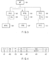
- FIG. 7 is a flowchart for explaining the procedure of the selecting process for the select command in the IC card 2.
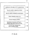
- the control element 21 of the IC card 2 has received a select command requesting the selection of a given DF from the IC card processor 1 by the communication unit 25. If the control element 21 of the IC card 2 has received a select command having normal parameters (OK in step S803), the control element 21 recognizes that the received command is a select command by "CLA” and "INS" of the received command, and starts a selecting process of setting the DF designated by "P1", "P2", and "Data" in the selected state.
Landscapes
- Engineering & Computer Science (AREA)
- Theoretical Computer Science (AREA)
- Computer Security & Cryptography (AREA)
- Computer Hardware Design (AREA)
- General Physics & Mathematics (AREA)
- General Engineering & Computer Science (AREA)
- Physics & Mathematics (AREA)
- Software Systems (AREA)
- Health & Medical Sciences (AREA)
- Bioethics (AREA)
- General Health & Medical Sciences (AREA)
- Databases & Information Systems (AREA)
- Storage Device Security (AREA)
- Information Retrieval, Db Structures And Fs Structures Therefor (AREA)
Claims (9)
- Carte à circuit intégré (2) comprenant :une unité de communication (25) configurée pour effectuer une communication de données avec un appareil externe ;une mémoire de données (22) configurée pour stocker des fichiers gérés par une structure hiérarchique, un dossier comme une couche supérieure des fichiers, et des informations concernant un héritage d'un état de sécurité entre une pluralité de dossiers ;un sélecteur (21) configuré pour mettre, si une commande demandant une sélection d'un deuxième dossier est reçue par l'unité de communication alors qu'un premier dossier est sélectionné, le premier dossier dans un état non sélectionné et le deuxième dossier désigné par la commande dans un état sélectionné ; etune unité d'héritage (21) configurée pour hériter, même lorsque le deuxième dossier est sélectionné, d'un état de sécurité établi alors que le premier dossier est sélectionné, si des informations indiquant un héritage de l'état de sécurité du premier dossier au deuxième dossier existent,caractérisée en ce quela mémoire de données est configurée pour stocker des informations indiquant une source d'héritage d'un état de sécurité dans des informations de commande de chaque dossier, etl'unité d'héritage est configurée pour hériter, même si le deuxième dossier est sélectionné, d'une condition de sécurité établie alors que le premier dossier est sélectionné, si des informations indiquant que le premier dossier est une source d'héritage de la condition de sécurité existent dans les informations de commande du deuxième dossier.
- Carte à circuit intégré (2) comprenant :une unité de communication (25) configurée pour effectuer une communication de données avec un appareil externe ;une mémoire de données (22) configurée pour stocker des fichiers gérés par une structure hiérarchique, un dossier comme une couche supérieure des fichiers, et des informations concernant un héritage d'un état de sécurité entre une pluralité de dossiers ;un sélecteur (21) configuré pour mettre, si une commande demandant une sélection d'un deuxième dossier est reçue par l'unité de communication alors qu'un premier dossier est sélectionné, le premier dossier dans un état non sélectionné et le deuxième dossier désigné par la commande dans un état sélectionné ; etune unité d'héritage (21) configurée pour hériter, même lorsque le deuxième dossier est sélectionné, d'un état de sécurité établi alors que le premier dossier est sélectionné, si des informations indiquant un héritage de l'état de sécurité du premier dossier au deuxième dossier existent,caractérisée en ce quela mémoire de données est configurée pour stocker des informations indiquant une destination d'héritage d'un état de sécurité dans des informations de commande de chaque dossier, etl'unité d'héritage est configurée pour hériter, même si le deuxième dossier est sélectionné, d'une condition de sécurité établie alors que le premier dossier est sélectionné, si des informations indiquant que le deuxième dossier est une destination d'héritage de la condition de sécurité existent dans les informations de commande du premier dossier.
- Carte selon la revendication 1 ou 2, caractérisée en ce que l'état de sécurité est une autorité obtenue par une réussite d'une parmi une authentification et une vérification à partir d'un appareil externe.
- Carte selon la revendication 1 ou 2, caractérisée en ce que l'état de sécurité est une clé pour l'utilisation dans une messagerie sécurisée.
- Carte selon la revendication 1 ou 2, caractérisée en ce que l'état de sécurité est le fait qu'une messagerie sécurisée peut être effectuée.
- Carte selon l'une quelconque des revendications 1 à 5, caractérisée en ce que l'unité d'héritage exécute un processus d'héritage sur la base d'une condition d'héritage d'état de sécurité contenue dans des informations concernant un héritage de l'état de sécurité.
- Carte selon l'une quelconque des revendications 1 à 6, caractérisée en ce qu'elle comprend :un module (M) incluant l'unité de communication, la mémoire de données, le sélecteur et l'unité d'héritage ; etun corps principal (B) incluant le module.
- Procédé de commande d'une carte à circuit intégré (2) comprenant :le stockage de fichiers gérés par une structure hiérarchique, d'un dossier comme une couche supérieure des fichiers et d'informations concernant un héritage d'un état de sécurité entre une pluralité de dossiers ;le réglage, si une commande demandant une sélection d'un deuxième dossier est reçue par l'unité de communication alors qu'un premier dossier est sélectionné, du premier dossier dans un état non sélectionné et du deuxième dossier désigné par la commande dans un état sélectionné ; etl'héritage, même lorsque le deuxième dossier est sélectionné, d'un état de sécurité établi alors que le premier dossier est sélectionné, si des informations indiquant un héritage de l'état de sécurité du premier dossier au deuxième dossier existent,caractérisé en ce quele stockage comprend le stockage d'informations indiquant une source d'héritage d'un état de sécurité dans des informations de commande de chaque dossier, etl'héritage comprend l'héritage, même si le deuxième dossier est sélectionné, d'une condition de sécurité établie alors que le premier dossier est sélectionné, si des informations indiquant que le premier dossier est une source d'héritage de la condition de sécurité existent dans les informations de commande du deuxième dossier.
- Procédé de commande d'une carte à circuit intégré (2) comprenant :le stockage de fichiers gérés par une structure hiérarchique, d'un dossier comme une couche supérieure des fichiers, et d'informations concernant un héritage d'un état de sécurité entre une pluralité de dossiers ;le réglage, si une commande demandant une sélection d'un deuxième dossier est reçue par l'unité de communication alors qu'un premier dossier est sélectionné, du premier dossier dans un état non sélectionné et du deuxième dossier désigné par la commande dans un état sélectionné ; etl'héritage, même lorsque le deuxième dossier est sélectionné, d'un état de sécurité établi alors que le premier dossier est sélectionné, si des informations indiquant un héritage de l'état de sécurité du premier dossier au deuxième dossier existent,caractérisé en ce quele stockage comprend le stockage d'informations indiquant une destination d'héritage d'un état de sécurité dans des informations de commande de chaque dossier, etl'héritage comprend l'héritage, même si le deuxième dossier est sélectionné, d'une condition de sécurité établie alors que le premier dossier est sélectionné, si des informations indiquant que le deuxième dossier est une destination d'héritage de la condition de sécurité existent dans les informations de commande du premier dossier.
Applications Claiming Priority (1)
| Application Number | Priority Date | Filing Date | Title |
|---|---|---|---|
| JP2012063365A JP5843674B2 (ja) | 2012-03-21 | 2012-03-21 | Icカード、携帯可能電子装置及びicカードの制御方法 |
Publications (3)
| Publication Number | Publication Date |
|---|---|
| EP2642422A2 EP2642422A2 (fr) | 2013-09-25 |
| EP2642422A3 EP2642422A3 (fr) | 2016-10-26 |
| EP2642422B1 true EP2642422B1 (fr) | 2018-04-25 |
Family
ID=48044535
Family Applications (1)
| Application Number | Title | Priority Date | Filing Date |
|---|---|---|---|
| EP13158932.7A Active EP2642422B1 (fr) | 2012-03-21 | 2013-03-13 | Carte à circuit intégré et procédé de commande de carte à circuit intégré |
Country Status (3)
| Country | Link |
|---|---|
| US (1) | US9183400B2 (fr) |
| EP (1) | EP2642422B1 (fr) |
| JP (1) | JP5843674B2 (fr) |
Families Citing this family (9)
| Publication number | Priority date | Publication date | Assignee | Title |
|---|---|---|---|---|
| JP6833364B2 (ja) * | 2016-07-01 | 2021-02-24 | 株式会社東芝 | Icカード、および、icカード処理装置 |
| US11281624B1 (en) | 2016-09-28 | 2022-03-22 | Amazon Technologies, Inc. | Client-based batching of data payload |
| US10496327B1 (en) | 2016-09-28 | 2019-12-03 | Amazon Technologies, Inc. | Command parallelization for data storage systems |
| US10810157B1 (en) * | 2016-09-28 | 2020-10-20 | Amazon Technologies, Inc. | Command aggregation for data storage operations |
| US11204895B1 (en) | 2016-09-28 | 2021-12-21 | Amazon Technologies, Inc. | Data payload clustering for data storage systems |
| US10657097B1 (en) | 2016-09-28 | 2020-05-19 | Amazon Technologies, Inc. | Data payload aggregation for data storage systems |
| US10437790B1 (en) | 2016-09-28 | 2019-10-08 | Amazon Technologies, Inc. | Contextual optimization for data storage systems |
| JP2018190194A (ja) * | 2017-05-08 | 2018-11-29 | 凸版印刷株式会社 | Icカード及びicカードの制御方法 |
| JP7020969B2 (ja) * | 2018-03-16 | 2022-02-16 | 株式会社東芝 | 携帯可能電子装置、及びicカード |
Family Cites Families (6)
| Publication number | Priority date | Publication date | Assignee | Title |
|---|---|---|---|---|
| JP3565481B2 (ja) * | 1998-11-19 | 2004-09-15 | 株式会社エヌ・ティ・ティ・データ | コンピュータのディレクトリアクセス制御システム及び方法 |
| JP2002312741A (ja) | 2001-04-10 | 2002-10-25 | Ntt Data Corp | Icカード及びプログラム |
| JP2005128996A (ja) * | 2003-09-30 | 2005-05-19 | Dainippon Printing Co Ltd | 情報処理装置、情報処理システム及びプログラム |
| JP4828809B2 (ja) * | 2003-12-10 | 2011-11-30 | 株式会社東芝 | Icカードおよびicカードにおける処理方法 |
| JP4891587B2 (ja) * | 2005-09-30 | 2012-03-07 | 株式会社東芝 | 携帯可能電子装置、icカードおよびicモジュール |
| JP5329884B2 (ja) * | 2008-09-18 | 2013-10-30 | 株式会社東芝 | 携帯可能電子装置および携帯可能電子装置におけるデータ処理方法 |
-
2012
- 2012-03-21 JP JP2012063365A patent/JP5843674B2/ja active Active
-
2013
- 2013-03-12 US US13/794,991 patent/US9183400B2/en active Active
- 2013-03-13 EP EP13158932.7A patent/EP2642422B1/fr active Active
Non-Patent Citations (1)
| Title |
|---|
| None * |
Also Published As
| Publication number | Publication date |
|---|---|
| JP2013196436A (ja) | 2013-09-30 |
| JP5843674B2 (ja) | 2016-01-13 |
| US9183400B2 (en) | 2015-11-10 |
| EP2642422A2 (fr) | 2013-09-25 |
| EP2642422A3 (fr) | 2016-10-26 |
| US20130254904A1 (en) | 2013-09-26 |
Similar Documents
| Publication | Publication Date | Title |
|---|---|---|
| EP2642422B1 (fr) | Carte à circuit intégré et procédé de commande de carte à circuit intégré | |
| JP5329884B2 (ja) | 携帯可能電子装置および携帯可能電子装置におけるデータ処理方法 | |
| US7775423B2 (en) | Portable electronic device and control method of portable electronic device | |
| US20120067947A1 (en) | Ic card, mobile electronic device and data processing method in ic card | |
| US10498671B2 (en) | IC card, portable electronic apparatus, and IC card processing apparatus | |
| US20090177921A1 (en) | Portable electronic device and control method thereof | |
| JP2010211516A (ja) | 携帯可能電子装置および携帯可能電子装置におけるアクセス制御方法 | |
| KR100399603B1 (ko) | 스마트 카드와 이의 os 프로그램 저장/삭제 및 실행방법 | |
| JP6984328B2 (ja) | 電子情報記憶媒体、icカード、外部機器、データ書き込み方法及びデータ書き込みプログラム | |
| US20090083273A1 (en) | Portable electronic apparatus and control method for portable electronic apparatus | |
| JP6039036B2 (ja) | Icカード、携帯可能電子装置及びicカードの制御方法 | |
| JP5957347B2 (ja) | Icカード、および携帯可能電子装置 | |
| JP7631895B2 (ja) | Icカード | |
| EP2642411B1 (fr) | Carte à circuit intégré et procédé de traitement de commande pour carte à circuit intégré | |
| JP5932588B2 (ja) | Icカード、携帯可能電子装置、及びicカード処理装置 | |
| JP6071677B2 (ja) | Icカード、icモジュールおよび携帯可能電子装置 | |
| JP2012133656A (ja) | 携帯可能電子装置及びicカード | |
| JP4533665B2 (ja) | 携帯可能電子装置 | |
| EP3144905B1 (fr) | Carte à circuit intégré et module de circuit intégré | |
| JP5038918B2 (ja) | 携帯可能電子装置および携帯可能電子装置の制御方法 | |
| JP2024139134A (ja) | 電子情報記憶媒体、icチップ、発行データの書き込み方法、及びプログラム | |
| JP2006293706A (ja) | アプリケーションの更新機能を有するマルチアプリケーションicカード | |
| JP2014182639A (ja) | Icカードおよび携帯可能電子装置 | |
| JP2014006631A (ja) | Icカード、および、携帯可能電子装置 | |
| JP2008242998A (ja) | Icカード |
Legal Events
| Date | Code | Title | Description |
|---|---|---|---|
| PUAI | Public reference made under article 153(3) epc to a published international application that has entered the european phase |
Free format text: ORIGINAL CODE: 0009012 |
|
| 17P | Request for examination filed |
Effective date: 20130313 |
|
| AK | Designated contracting states |
Kind code of ref document: A2 Designated state(s): AL AT BE BG CH CY CZ DE DK EE ES FI FR GB GR HR HU IE IS IT LI LT LU LV MC MK MT NL NO PL PT RO RS SE SI SK SM TR |
|
| AX | Request for extension of the european patent |
Extension state: BA ME |
|
| PUAL | Search report despatched |
Free format text: ORIGINAL CODE: 0009013 |
|
| AK | Designated contracting states |
Kind code of ref document: A3 Designated state(s): AL AT BE BG CH CY CZ DE DK EE ES FI FR GB GR HR HU IE IS IT LI LT LU LV MC MK MT NL NO PL PT RO RS SE SI SK SM TR |
|
| AX | Request for extension of the european patent |
Extension state: BA ME |
|
| RIC1 | Information provided on ipc code assigned before grant |
Ipc: G06F 21/60 20130101ALI20160916BHEP Ipc: G06F 21/62 20130101ALI20160916BHEP Ipc: G06F 21/79 20130101AFI20160916BHEP |
|
| STAA | Information on the status of an ep patent application or granted ep patent |
Free format text: STATUS: EXAMINATION IS IN PROGRESS |
|
| 17Q | First examination report despatched |
Effective date: 20170620 |
|
| GRAP | Despatch of communication of intention to grant a patent |
Free format text: ORIGINAL CODE: EPIDOSNIGR1 |
|
| STAA | Information on the status of an ep patent application or granted ep patent |
Free format text: STATUS: GRANT OF PATENT IS INTENDED |
|
| INTG | Intention to grant announced |
Effective date: 20171113 |
|
| GRAS | Grant fee paid |
Free format text: ORIGINAL CODE: EPIDOSNIGR3 |
|
| GRAA | (expected) grant |
Free format text: ORIGINAL CODE: 0009210 |
|
| STAA | Information on the status of an ep patent application or granted ep patent |
Free format text: STATUS: THE PATENT HAS BEEN GRANTED |
|
| AK | Designated contracting states |
Kind code of ref document: B1 Designated state(s): AL AT BE BG CH CY CZ DE DK EE ES FI FR GB GR HR HU IE IS IT LI LT LU LV MC MK MT NL NO PL PT RO RS SE SI SK SM TR |
|
| REG | Reference to a national code |
Ref country code: GB Ref legal event code: FG4D |
|
| REG | Reference to a national code |
Ref country code: CH Ref legal event code: EP |
|
| REG | Reference to a national code |
Ref country code: AT Ref legal event code: REF Ref document number: 993648 Country of ref document: AT Kind code of ref document: T Effective date: 20180515 |
|
| REG | Reference to a national code |
Ref country code: IE Ref legal event code: FG4D |
|
| REG | Reference to a national code |
Ref country code: DE Ref legal event code: R096 Ref document number: 602013036339 Country of ref document: DE |
|
| REG | Reference to a national code |
Ref country code: NL Ref legal event code: MP Effective date: 20180425 |
|
| REG | Reference to a national code |
Ref country code: LT Ref legal event code: MG4D |
|
| PG25 | Lapsed in a contracting state [announced via postgrant information from national office to epo] |
Ref country code: NL Free format text: LAPSE BECAUSE OF FAILURE TO SUBMIT A TRANSLATION OF THE DESCRIPTION OR TO PAY THE FEE WITHIN THE PRESCRIBED TIME-LIMIT Effective date: 20180425 |
|
| PG25 | Lapsed in a contracting state [announced via postgrant information from national office to epo] |
Ref country code: PL Free format text: LAPSE BECAUSE OF FAILURE TO SUBMIT A TRANSLATION OF THE DESCRIPTION OR TO PAY THE FEE WITHIN THE PRESCRIBED TIME-LIMIT Effective date: 20180425 Ref country code: NO Free format text: LAPSE BECAUSE OF FAILURE TO SUBMIT A TRANSLATION OF THE DESCRIPTION OR TO PAY THE FEE WITHIN THE PRESCRIBED TIME-LIMIT Effective date: 20180725 Ref country code: SE Free format text: LAPSE BECAUSE OF FAILURE TO SUBMIT A TRANSLATION OF THE DESCRIPTION OR TO PAY THE FEE WITHIN THE PRESCRIBED TIME-LIMIT Effective date: 20180425 Ref country code: FI Free format text: LAPSE BECAUSE OF FAILURE TO SUBMIT A TRANSLATION OF THE DESCRIPTION OR TO PAY THE FEE WITHIN THE PRESCRIBED TIME-LIMIT Effective date: 20180425 Ref country code: BG Free format text: LAPSE BECAUSE OF FAILURE TO SUBMIT A TRANSLATION OF THE DESCRIPTION OR TO PAY THE FEE WITHIN THE PRESCRIBED TIME-LIMIT Effective date: 20180725 Ref country code: ES Free format text: LAPSE BECAUSE OF FAILURE TO SUBMIT A TRANSLATION OF THE DESCRIPTION OR TO PAY THE FEE WITHIN THE PRESCRIBED TIME-LIMIT Effective date: 20180425 Ref country code: LT Free format text: LAPSE BECAUSE OF FAILURE TO SUBMIT A TRANSLATION OF THE DESCRIPTION OR TO PAY THE FEE WITHIN THE PRESCRIBED TIME-LIMIT Effective date: 20180425 |
|
| PG25 | Lapsed in a contracting state [announced via postgrant information from national office to epo] |
Ref country code: LV Free format text: LAPSE BECAUSE OF FAILURE TO SUBMIT A TRANSLATION OF THE DESCRIPTION OR TO PAY THE FEE WITHIN THE PRESCRIBED TIME-LIMIT Effective date: 20180425 Ref country code: HR Free format text: LAPSE BECAUSE OF FAILURE TO SUBMIT A TRANSLATION OF THE DESCRIPTION OR TO PAY THE FEE WITHIN THE PRESCRIBED TIME-LIMIT Effective date: 20180425 Ref country code: GR Free format text: LAPSE BECAUSE OF FAILURE TO SUBMIT A TRANSLATION OF THE DESCRIPTION OR TO PAY THE FEE WITHIN THE PRESCRIBED TIME-LIMIT Effective date: 20180726 Ref country code: RS Free format text: LAPSE BECAUSE OF FAILURE TO SUBMIT A TRANSLATION OF THE DESCRIPTION OR TO PAY THE FEE WITHIN THE PRESCRIBED TIME-LIMIT Effective date: 20180425 |
|
| REG | Reference to a national code |
Ref country code: AT Ref legal event code: MK05 Ref document number: 993648 Country of ref document: AT Kind code of ref document: T Effective date: 20180425 |
|
| PG25 | Lapsed in a contracting state [announced via postgrant information from national office to epo] |
Ref country code: PT Free format text: LAPSE BECAUSE OF FAILURE TO SUBMIT A TRANSLATION OF THE DESCRIPTION OR TO PAY THE FEE WITHIN THE PRESCRIBED TIME-LIMIT Effective date: 20180827 |
|
| REG | Reference to a national code |
Ref country code: DE Ref legal event code: R097 Ref document number: 602013036339 Country of ref document: DE |
|
| PG25 | Lapsed in a contracting state [announced via postgrant information from national office to epo] |
Ref country code: AT Free format text: LAPSE BECAUSE OF FAILURE TO SUBMIT A TRANSLATION OF THE DESCRIPTION OR TO PAY THE FEE WITHIN THE PRESCRIBED TIME-LIMIT Effective date: 20180425 Ref country code: DK Free format text: LAPSE BECAUSE OF FAILURE TO SUBMIT A TRANSLATION OF THE DESCRIPTION OR TO PAY THE FEE WITHIN THE PRESCRIBED TIME-LIMIT Effective date: 20180425 Ref country code: EE Free format text: LAPSE BECAUSE OF FAILURE TO SUBMIT A TRANSLATION OF THE DESCRIPTION OR TO PAY THE FEE WITHIN THE PRESCRIBED TIME-LIMIT Effective date: 20180425 Ref country code: RO Free format text: LAPSE BECAUSE OF FAILURE TO SUBMIT A TRANSLATION OF THE DESCRIPTION OR TO PAY THE FEE WITHIN THE PRESCRIBED TIME-LIMIT Effective date: 20180425 Ref country code: CZ Free format text: LAPSE BECAUSE OF FAILURE TO SUBMIT A TRANSLATION OF THE DESCRIPTION OR TO PAY THE FEE WITHIN THE PRESCRIBED TIME-LIMIT Effective date: 20180425 Ref country code: SK Free format text: LAPSE BECAUSE OF FAILURE TO SUBMIT A TRANSLATION OF THE DESCRIPTION OR TO PAY THE FEE WITHIN THE PRESCRIBED TIME-LIMIT Effective date: 20180425 |
|
| PG25 | Lapsed in a contracting state [announced via postgrant information from national office to epo] |
Ref country code: SM Free format text: LAPSE BECAUSE OF FAILURE TO SUBMIT A TRANSLATION OF THE DESCRIPTION OR TO PAY THE FEE WITHIN THE PRESCRIBED TIME-LIMIT Effective date: 20180425 Ref country code: IT Free format text: LAPSE BECAUSE OF FAILURE TO SUBMIT A TRANSLATION OF THE DESCRIPTION OR TO PAY THE FEE WITHIN THE PRESCRIBED TIME-LIMIT Effective date: 20180425 |
|
| PLBE | No opposition filed within time limit |
Free format text: ORIGINAL CODE: 0009261 |
|
| STAA | Information on the status of an ep patent application or granted ep patent |
Free format text: STATUS: NO OPPOSITION FILED WITHIN TIME LIMIT |
|
| 26N | No opposition filed |
Effective date: 20190128 |
|
| PG25 | Lapsed in a contracting state [announced via postgrant information from national office to epo] |
Ref country code: SI Free format text: LAPSE BECAUSE OF FAILURE TO SUBMIT A TRANSLATION OF THE DESCRIPTION OR TO PAY THE FEE WITHIN THE PRESCRIBED TIME-LIMIT Effective date: 20180425 |
|
| PG25 | Lapsed in a contracting state [announced via postgrant information from national office to epo] |
Ref country code: MC Free format text: LAPSE BECAUSE OF FAILURE TO SUBMIT A TRANSLATION OF THE DESCRIPTION OR TO PAY THE FEE WITHIN THE PRESCRIBED TIME-LIMIT Effective date: 20180425 |
|
| REG | Reference to a national code |
Ref country code: CH Ref legal event code: PL |
|
| GBPC | Gb: european patent ceased through non-payment of renewal fee |
Effective date: 20190313 |
|
| PG25 | Lapsed in a contracting state [announced via postgrant information from national office to epo] |
Ref country code: AL Free format text: LAPSE BECAUSE OF FAILURE TO SUBMIT A TRANSLATION OF THE DESCRIPTION OR TO PAY THE FEE WITHIN THE PRESCRIBED TIME-LIMIT Effective date: 20180425 Ref country code: LU Free format text: LAPSE BECAUSE OF NON-PAYMENT OF DUE FEES Effective date: 20190313 |
|
| REG | Reference to a national code |
Ref country code: BE Ref legal event code: MM Effective date: 20190331 |
|
| PG25 | Lapsed in a contracting state [announced via postgrant information from national office to epo] |
Ref country code: LI Free format text: LAPSE BECAUSE OF NON-PAYMENT OF DUE FEES Effective date: 20190331 Ref country code: IE Free format text: LAPSE BECAUSE OF NON-PAYMENT OF DUE FEES Effective date: 20190313 Ref country code: CH Free format text: LAPSE BECAUSE OF NON-PAYMENT OF DUE FEES Effective date: 20190331 Ref country code: GB Free format text: LAPSE BECAUSE OF NON-PAYMENT OF DUE FEES Effective date: 20190313 |
|
| PG25 | Lapsed in a contracting state [announced via postgrant information from national office to epo] |
Ref country code: BE Free format text: LAPSE BECAUSE OF NON-PAYMENT OF DUE FEES Effective date: 20190331 |
|
| PG25 | Lapsed in a contracting state [announced via postgrant information from national office to epo] |
Ref country code: TR Free format text: LAPSE BECAUSE OF FAILURE TO SUBMIT A TRANSLATION OF THE DESCRIPTION OR TO PAY THE FEE WITHIN THE PRESCRIBED TIME-LIMIT Effective date: 20180425 |
|
| PG25 | Lapsed in a contracting state [announced via postgrant information from national office to epo] |
Ref country code: MT Free format text: LAPSE BECAUSE OF NON-PAYMENT OF DUE FEES Effective date: 20190313 |
|
| PG25 | Lapsed in a contracting state [announced via postgrant information from national office to epo] |
Ref country code: CY Free format text: LAPSE BECAUSE OF FAILURE TO SUBMIT A TRANSLATION OF THE DESCRIPTION OR TO PAY THE FEE WITHIN THE PRESCRIBED TIME-LIMIT Effective date: 20180425 |
|
| PG25 | Lapsed in a contracting state [announced via postgrant information from national office to epo] |
Ref country code: IS Free format text: LAPSE BECAUSE OF FAILURE TO SUBMIT A TRANSLATION OF THE DESCRIPTION OR TO PAY THE FEE WITHIN THE PRESCRIBED TIME-LIMIT Effective date: 20180825 |
|
| PG25 | Lapsed in a contracting state [announced via postgrant information from national office to epo] |
Ref country code: HU Free format text: LAPSE BECAUSE OF FAILURE TO SUBMIT A TRANSLATION OF THE DESCRIPTION OR TO PAY THE FEE WITHIN THE PRESCRIBED TIME-LIMIT; INVALID AB INITIO Effective date: 20130313 |
|
| PG25 | Lapsed in a contracting state [announced via postgrant information from national office to epo] |
Ref country code: MK Free format text: LAPSE BECAUSE OF FAILURE TO SUBMIT A TRANSLATION OF THE DESCRIPTION OR TO PAY THE FEE WITHIN THE PRESCRIBED TIME-LIMIT Effective date: 20180425 |
|
| PGFP | Annual fee paid to national office [announced via postgrant information from national office to epo] |
Ref country code: FR Payment date: 20251231 Year of fee payment: 14 |
|
| PGFP | Annual fee paid to national office [announced via postgrant information from national office to epo] |
Ref country code: DE Payment date: 20260102 Year of fee payment: 14 |