EP2645142A1 - Opto-electric hybrid board - Google Patents
Opto-electric hybrid board Download PDFInfo
- Publication number
- EP2645142A1 EP2645142A1 EP13157566.4A EP13157566A EP2645142A1 EP 2645142 A1 EP2645142 A1 EP 2645142A1 EP 13157566 A EP13157566 A EP 13157566A EP 2645142 A1 EP2645142 A1 EP 2645142A1
- Authority
- EP
- European Patent Office
- Prior art keywords
- insulative layer
- light
- opto
- electric hybrid
- hybrid board
- Prior art date
- Legal status (The legal status is an assumption and is not a legal conclusion. Google has not performed a legal analysis and makes no representation as to the accuracy of the status listed.)
- Withdrawn
Links
- 230000003287 optical effect Effects 0.000 claims abstract description 88
- 239000000463 material Substances 0.000 claims abstract description 20
- 238000000034 method Methods 0.000 claims description 25
- 238000002834 transmittance Methods 0.000 claims description 9
- 239000011347 resin Substances 0.000 claims description 7
- 229920005989 resin Polymers 0.000 claims description 7
- 229910052751 metal Inorganic materials 0.000 description 40
- 239000002184 metal Substances 0.000 description 40
- 238000005253 cladding Methods 0.000 description 28
- 230000015572 biosynthetic process Effects 0.000 description 12
- HEMHJVSKTPXQMS-UHFFFAOYSA-M Sodium hydroxide Chemical compound [OH-].[Na+] HEMHJVSKTPXQMS-UHFFFAOYSA-M 0.000 description 6
- 239000000853 adhesive Substances 0.000 description 6
- 230000001070 adhesive effect Effects 0.000 description 6
- 230000008878 coupling Effects 0.000 description 6
- 238000010168 coupling process Methods 0.000 description 6
- 238000005859 coupling reaction Methods 0.000 description 6
- 238000005530 etching Methods 0.000 description 6
- 230000000052 comparative effect Effects 0.000 description 5
- 230000000694 effects Effects 0.000 description 5
- PXHVJJICTQNCMI-UHFFFAOYSA-N Nickel Chemical compound [Ni] PXHVJJICTQNCMI-UHFFFAOYSA-N 0.000 description 4
- 238000010329 laser etching Methods 0.000 description 4
- 238000000465 moulding Methods 0.000 description 4
- 229920001721 polyimide Polymers 0.000 description 4
- 239000010935 stainless steel Substances 0.000 description 4
- 229910001220 stainless steel Inorganic materials 0.000 description 4
- 239000000654 additive Substances 0.000 description 3
- 230000003247 decreasing effect Effects 0.000 description 3
- RYGMFSIKBFXOCR-UHFFFAOYSA-N Copper Chemical compound [Cu] RYGMFSIKBFXOCR-UHFFFAOYSA-N 0.000 description 2
- 239000004642 Polyimide Substances 0.000 description 2
- 229910052802 copper Inorganic materials 0.000 description 2
- 239000010949 copper Substances 0.000 description 2
- 238000009713 electroplating Methods 0.000 description 2
- 238000004519 manufacturing process Methods 0.000 description 2
- 229910052759 nickel Inorganic materials 0.000 description 2
- -1 polyethylene terephthalate Polymers 0.000 description 2
- 239000009719 polyimide resin Substances 0.000 description 2
- 229920003002 synthetic resin Polymers 0.000 description 2
- 239000000057 synthetic resin Substances 0.000 description 2
- 239000004925 Acrylic resin Substances 0.000 description 1
- 229920000178 Acrylic resin Polymers 0.000 description 1
- VYZAMTAEIAYCRO-UHFFFAOYSA-N Chromium Chemical compound [Cr] VYZAMTAEIAYCRO-UHFFFAOYSA-N 0.000 description 1
- 229910021578 Iron(III) chloride Inorganic materials 0.000 description 1
- 239000004695 Polyether sulfone Substances 0.000 description 1
- 239000004721 Polyphenylene oxide Substances 0.000 description 1
- 239000000956 alloy Substances 0.000 description 1
- 229910045601 alloy Inorganic materials 0.000 description 1
- 230000005540 biological transmission Effects 0.000 description 1
- 229910052804 chromium Inorganic materials 0.000 description 1
- 239000011651 chromium Substances 0.000 description 1
- 238000005520 cutting process Methods 0.000 description 1
- 238000007772 electroless plating Methods 0.000 description 1
- 239000003822 epoxy resin Substances 0.000 description 1
- 239000011888 foil Substances 0.000 description 1
- PCHJSUWPFVWCPO-UHFFFAOYSA-N gold Chemical compound [Au] PCHJSUWPFVWCPO-UHFFFAOYSA-N 0.000 description 1
- 229910052737 gold Inorganic materials 0.000 description 1
- 239000010931 gold Substances 0.000 description 1
- LNEPOXFFQSENCJ-UHFFFAOYSA-N haloperidol Chemical compound C1CC(O)(C=2C=CC(Cl)=CC=2)CCN1CCCC(=O)C1=CC=C(F)C=C1 LNEPOXFFQSENCJ-UHFFFAOYSA-N 0.000 description 1
- RBTARNINKXHZNM-UHFFFAOYSA-K iron trichloride Chemical compound Cl[Fe](Cl)Cl RBTARNINKXHZNM-UHFFFAOYSA-K 0.000 description 1
- 238000003754 machining Methods 0.000 description 1
- 239000007769 metal material Substances 0.000 description 1
- 239000000203 mixture Substances 0.000 description 1
- 238000012986 modification Methods 0.000 description 1
- 230000004048 modification Effects 0.000 description 1
- 150000002825 nitriles Chemical class 0.000 description 1
- 229920001568 phenolic resin Polymers 0.000 description 1
- 239000005011 phenolic resin Substances 0.000 description 1
- 239000004033 plastic Substances 0.000 description 1
- 229920003023 plastic Polymers 0.000 description 1
- 229920003207 poly(ethylene-2,6-naphthalate) Polymers 0.000 description 1
- 229920000647 polyepoxide Polymers 0.000 description 1
- 229920000570 polyether Polymers 0.000 description 1
- 229920006393 polyether sulfone Polymers 0.000 description 1
- 239000011112 polyethylene naphthalate Substances 0.000 description 1
- 229920000139 polyethylene terephthalate Polymers 0.000 description 1
- 239000005020 polyethylene terephthalate Substances 0.000 description 1
- 229920000915 polyvinyl chloride Polymers 0.000 description 1
- 239000004800 polyvinyl chloride Substances 0.000 description 1
- 230000000452 restraining effect Effects 0.000 description 1
- 238000004544 sputter deposition Methods 0.000 description 1
- 238000012360 testing method Methods 0.000 description 1
Images


Classifications
-
- G—PHYSICS
- G02—OPTICS
- G02B—OPTICAL ELEMENTS, SYSTEMS OR APPARATUS
- G02B6/00—Light guides; Structural details of arrangements comprising light guides and other optical elements, e.g. couplings
- G02B6/10—Light guides; Structural details of arrangements comprising light guides and other optical elements, e.g. couplings of the optical waveguide type
-
- G—PHYSICS
- G02—OPTICS
- G02B—OPTICAL ELEMENTS, SYSTEMS OR APPARATUS
- G02B6/00—Light guides; Structural details of arrangements comprising light guides and other optical elements, e.g. couplings
- G02B6/24—Coupling light guides
- G02B6/42—Coupling light guides with opto-electronic elements
- G02B6/4201—Packages, e.g. shape, construction, internal or external details
- G02B6/4204—Packages, e.g. shape, construction, internal or external details the coupling comprising intermediate optical elements, e.g. lenses, holograms
- G02B6/4214—Packages, e.g. shape, construction, internal or external details the coupling comprising intermediate optical elements, e.g. lenses, holograms the intermediate optical element having redirecting reflective means, e.g. mirrors, prisms for deflecting the radiation from horizontal to down- or upward direction toward a device
-
- G—PHYSICS
- G02—OPTICS
- G02B—OPTICAL ELEMENTS, SYSTEMS OR APPARATUS
- G02B6/00—Light guides; Structural details of arrangements comprising light guides and other optical elements, e.g. couplings
- G02B6/24—Coupling light guides
- G02B6/42—Coupling light guides with opto-electronic elements
- G02B6/4201—Packages, e.g. shape, construction, internal or external details
- G02B6/4204—Packages, e.g. shape, construction, internal or external details the coupling comprising intermediate optical elements, e.g. lenses, holograms
-
- G—PHYSICS
- G02—OPTICS
- G02B—OPTICAL ELEMENTS, SYSTEMS OR APPARATUS
- G02B6/00—Light guides; Structural details of arrangements comprising light guides and other optical elements, e.g. couplings
- G02B6/24—Coupling light guides
- G02B6/42—Coupling light guides with opto-electronic elements
- G02B6/4201—Packages, e.g. shape, construction, internal or external details
- G02B6/4204—Packages, e.g. shape, construction, internal or external details the coupling comprising intermediate optical elements, e.g. lenses, holograms
- G02B6/4206—Optical features
-
- H—ELECTRICITY
- H05—ELECTRIC TECHNIQUES NOT OTHERWISE PROVIDED FOR
- H05K—PRINTED CIRCUITS; CASINGS OR CONSTRUCTIONAL DETAILS OF ELECTRIC APPARATUS; MANUFACTURE OF ASSEMBLAGES OF ELECTRICAL COMPONENTS
- H05K1/00—Printed circuits
- H05K1/02—Details
-
- H—ELECTRICITY
- H05—ELECTRIC TECHNIQUES NOT OTHERWISE PROVIDED FOR
- H05K—PRINTED CIRCUITS; CASINGS OR CONSTRUCTIONAL DETAILS OF ELECTRIC APPARATUS; MANUFACTURE OF ASSEMBLAGES OF ELECTRICAL COMPONENTS
- H05K1/00—Printed circuits
- H05K1/02—Details
- H05K1/0274—Optical details, e.g. printed circuits comprising integral optical means
-
- G—PHYSICS
- G02—OPTICS
- G02B—OPTICAL ELEMENTS, SYSTEMS OR APPARATUS
- G02B6/00—Light guides; Structural details of arrangements comprising light guides and other optical elements, e.g. couplings
- G02B6/24—Coupling light guides
- G02B6/42—Coupling light guides with opto-electronic elements
- G02B6/4201—Packages, e.g. shape, construction, internal or external details
- G02B6/4274—Electrical aspects
- G02B6/4283—Electrical aspects with electrical insulation means
-
- G—PHYSICS
- G02—OPTICS
- G02B—OPTICAL ELEMENTS, SYSTEMS OR APPARATUS
- G02B6/00—Light guides; Structural details of arrangements comprising light guides and other optical elements, e.g. couplings
- G02B6/24—Coupling light guides
- G02B6/42—Coupling light guides with opto-electronic elements
- G02B6/43—Arrangements comprising a plurality of opto-electronic elements and associated optical interconnections
-
- H—ELECTRICITY
- H05—ELECTRIC TECHNIQUES NOT OTHERWISE PROVIDED FOR
- H05K—PRINTED CIRCUITS; CASINGS OR CONSTRUCTIONAL DETAILS OF ELECTRIC APPARATUS; MANUFACTURE OF ASSEMBLAGES OF ELECTRICAL COMPONENTS
- H05K2201/00—Indexing scheme relating to printed circuits covered by H05K1/00
- H05K2201/10—Details of components or other objects attached to or integrated in a printed circuit board
- H05K2201/10007—Types of components
- H05K2201/10121—Optical component, e.g. opto-electronic component
Definitions
- the present invention relates to an opto-electric hybrid board in which an electric circuit board with an optical element mounted thereon and an optical waveguide are stacked together.
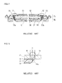
- this opto-electric hybrid board includes: an electric circuit board E 0 including an insulative layer 51, and electrical interconnect lines 52 formed on the front surface of the insulative layer 51; an optical waveguide (optical interconnect lines) W 0 (including an under cladding layer 56, cores 57 and an over cladding layer 58) stacked on the back surface (a surface opposite from the surface with the electrical interconnect lines 52 formed thereon) of the insulative layer 51 of the electric circuit board E 0 ; and a light-emitting element 11 and a light-receiving element 12 which are mounted on portions of the surface with the electrical interconnect lines 52 formed thereon, the portions corresponding to opposite end portions of the optical waveguide W 0 .
- the opposite end portions of the optical waveguide W 0 are formed into inclined surfaces inclined at 45 degrees with respect to the electric circuit board E 0 . Portions of each of the cores 57 positioned at the inclined surfaces function as first and second light reflecting surfaces 57a. Portions of the insulative layer 51 corresponding to the light-emitting element 11 and the light-receiving element 12 have first and second through holes 55, respectively, for an optical path.
- the first and second through holes 55 allow a light beam L to propagate therethrough between the light-emitting element 11 and the first light reflecting surface 57a provided in a first end portion of the optical waveguide W 0 and between the light-receiving element 12 and the second light reflecting surface 57a provided in a second end portion thereof.
- the propagation of the light beam L in the aforementioned opto-electric hybrid board is performed in a manner to be described below.
- the light beam L is emitted from the light-emitting element 11 toward the first light reflecting surface 57a.
- the light beam L passes through the first through hole 55 for an optical path formed in the insulative layer 51, and then passes through the under cladding layer 56 in the first end portion (the left-hand end portion as seen in FIG. 7 ) of the optical waveguide W 0 .
- the light beam L is reflected from the first light reflecting surface 57a of each of the cores 57 (or the optical path is changed by 90 degrees), and travels through the interior of each core 57 in an axial direction.
- the light beam L is reflected from the second light reflecting surface 57a provided in the second end portion (the right-hand end portion as seen in FIG. 7 ) of each core 57 (or the optical path is changed by 90 degrees), and travels toward the light-receiving element 12. Subsequently, the light beam L passes through the under cladding layer 56 in the second end portion, and travels outwardly of the optical waveguide W 0 . Then, the light beam L passes through the second through hole 55 for an optical path, and is received by the light-receiving element 12.
- Japanese Published Patent Application No. 2002-258081 discloses a technique in which a lens 60 is mounted to an opening surface of the second through hole 55 for an optical path to change the light beam L passing through the second through hole 55 into a collimated light beam or a convergent light beam by the effect of the lens 60, as shown in FIG. 8 .
- This technique changes the light beam L into a collimated light beam or a convergent light beam as mentioned above to achieve the efficient propagation of the light beam L.
- the lens 60 which is mounted, involves the need for the step of mounting the lens 60, resulting in a problem such that the productivity is lowered.
- the process of mounting the lens 60 also results in a problem such that variations occur in the accuracy of the position of the mounting.
- an opto-electric hybrid board which includes a lens formed in an optical path between an optical element and a core with stable positional accuracy without the decrease in productivity.
- the opto-electric hybrid board comprises: an electric circuit board including an insulative layer having front and back surfaces, and electrical interconnect lines formed on the front surface of the insulative layer; an optical element mounted on a surface of the electric circuit board with the electrical interconnect lines formed thereon; and an optical waveguide including a core and formed on the back surface of the insulative layer of the electric circuit board, the core including at its end portion a ref lecting portion capable of reflecting light to propagate the light between the core and the optical element, the insulative layer being made of a light-transmissive material, the insulative layer including a portion corresponding to an optical path between the reflecting portion of the core and the optical element, the corresponding portion of the insulative layer being in the form of a lens portion.
- the insulative layer is made of a light-transmissive material. This eliminates the need for the provision of a through hole for an optical path in a portion of the insulative layer corresponding to the optical path between the reflecting portion of the core and the optical element. Additionally, the portion of the insulative layer serving as the optical path is in the form of a lens portion. Thus, the lens portion is part of the insulative layer, and there is no need to mount a separate lens. In this manner, the opto-electric hybrid board eliminates the need for the step of forming a through hole for an optical path in the insulative layer and the step of mounting a lens in the optical path portion. This improves productivity. Further, since there is no need to mount a separate lens to the insulative layer as mentioned above, no variations occur in mounting position. This achieves the formation of the lens portion with stable positional accuracy.
- the light-transmissive material of the insulative layer is a photosensitive resin
- the lens portion is formed by gradation exposure during a photolithographic process.
- the insulative layer with the lens portion is formed by a single photolithographic process. Therefore, the opto-electric hybrid board is excellent in productivity and in the positional accuracy of the lens portion.
- the insulative layer includes alignment marks formed thereon for the positioning of the electrical interconnect lines, and the electrical interconnect lines are formed using the alignment marks as a guide.
- the opto-electric hybrid board is excellent also in the positional accuracy of the electrical interconnect lines.
- the insulative layer includes alignment marks formed thereon for the positioning of the optical element, and the optical element is mounted using the alignment marks as a guide.
- the opto-electric hybrid board is excellent also in the positional accuracy of the optical element.
- the insulative layer has a light transmittance of not less than 70% at a wavelength of not less than 600 nm. In such a case, a greater amount of light is transmitted through the insulative layer. Thus, the coupling loss of light is decreased.
- the insulative layer is a heat-resistant layer having resistance to heat at 150°C or higher.
- the lens portion is prevented from becoming deformed due to heat produced during the mounting of the optical element. This allows the lens to perform a proper light-gathering effect.
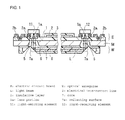
- FIG. 1 is a longitudinal sectional view schematically showing an opto-electric hybrid board according to a first preferred embodiment.
- the opto-electric hybrid board according to the first preferred embodiment is a strip-shaped opto-electric hybrid board extending leftwardly and rightwardly, and includes: an electric circuit board E including an insulative layer 1 having front and back surfaces, and electrical interconnect lines 2 formed on the front surface of the insulative layer 1; a light-emitting element 11 and a light-receiving element 12 which are mounted on a surface of the electric circuit board E with the electrical interconnect lines 2 formed thereon; an optical waveguide W formed on the back surface of the insulative layer 1 of the electric circuit board E; and a metal layer M formed between the optical waveguide W and the back surface of the insulative layer 1 of the electric circuit board E.
- the metal layer M has first and second through holes 5 for an optical path, which are in positions corresponding to the light-emitting element 11 and the light-receiving element 12, respectively.
- Notches of an inverted V shape are formed respectively in opposite end portions of the optical waveguide W corresponding to the light-emitting element 11 and the light-receiving element 12.
- Inclined surfaces of the inverted V-shaped notches are in the form of surfaces inclined at 45 degrees to the longitudinal direction of cores 7 of the optical waveguide W.
- the inclined surfaces serve as first and second reflecting surfaces 7a which reflect light beams to allow the propagation of the light beams between the light-emitting element 11 and each of the cores 7 and the propagation of the light beams between the light-receiving element 12 and each of the cores 7.
- the insulative layer 1 is made of a light-transmissive material such as a transparent synthetic resin.
- a portion of the insulative layer 1 corresponding to an optical path lying between the first reflecting surface 7a provided in a first end portion of each of the cores 7 and the light-emitting element 11 is in the form of a first lens portion 1a having a convex curved surface bulging toward the light-emitting element 11.
- a portion of the insulative layer 1 corresponding to an optical path lying between the second reflecting surface 7a provided in a second end portion of each of the cores 7 and the light-receiving element 12 is in the form of a second lens portion 1a similar to the first lens portion 1a.
- the insulative layer 1 itself is made of a light-transmissive material, and portions of the insulative layer 1 corresponding to the optical paths are in the form of the lens portions 1a.
- a light beam L is emitted in a diffused manner from the light-emitting element 11 toward the first reflecting surface 7a provided in the first end portion (the left-hand end portion as seen in FIG. 1 ) of each core 7.
- the light beam L initially passes through the first lens portion 1a of the insulative layer 1.
- the diffused light beam L is changed into a collimated light beam or a convergent light beam (a collimated light beam as seen in FIG. 1 ) by the effect of the first lens portion 1a.
- the light beam L After passing through the first through hole 5 formed in the metal layer M, the light beam L is reflected from the first reflecting surface 7a provided in the first end portion of each core 7, and travels through the interior of each core 7 in an axial direction. Then, the light beam L is reflected from the second reflecting surface 7a provided in the second end portion (the right-hand end portion as seen in FIG. 1 ) of each core 7, and passes through the second through hole 5 formed in the metal layer M and through the second lens portion 1a of the insulative layer 1. When the light beam L passes through the second lens portion 1a, the light beam L is changed into a convergent light beam by the effect of the second lens portion 1a. Then, the light beam L is received by the light-receiving element 12.
- the light beam L is changed into a collimated light beam or a convergent light beam by the effect of the first and second lens portions 1a of the insulative layer 1, when emitted from the light-emitting element 11 and entering the first end portion of each core 7 and when reflected from the second reflecting surface 7a provided in the second end portion of each core 7 and received by the light-receiving element 12.
- This achieves the efficient propagation of the light beam L.
- the opto-electric hybrid board is excellent in productivity and in the positional accuracy of the lens portions 1a.
- uncovered optical element mounting pads 2a are formed on the front surface of the insulative layer 1, and uncovered grounding electrodes 2b extend through the insulative layer 1 into contact with the metal layer M on the back surface of the insulative layer 1.
- the optical element mounting pads 2a and the grounding electrodes 2b are portions of the electrical interconnect lines 2. Portions of the electrical interconnect lines 2 other than the optical element mounting pads 2a and the grounding electrodes 2b are covered with a coverlay 3, and are insulated and protected.
- the optical waveguide W includes an under cladding layer 6, the cores 7 formed in a predetermined pattern on the front surface (the lower surface as seen in FIG. 1 ) of the under cladding layer 6, and an over cladding layer 8 formed on the front surface of the under cladding layer 6 so as to cover the cores 7.
- the under cladding layer 6 has a back surface (a surface opposite from the surface with the cores 7 formed thereon) in contact with the metal layer M, and enters and fills the first and second through holes 5 for an optical path formed in the metal layer M.
- the metal layer M of a flat configuration (with reference to FIG. 2A ) is prepared.
- a material for the formation of the metal layer M include stainless steel, and 42 alloy.
- stainless steel is preferable from the viewpoint of dimensional accuracy and the like.
- the metal layer M has a thickness in the range of 10 to 100 ⁇ m, for example.
- a photosensitive insulating resin is applied to the front surface of the metal layer M to form the insulative layer 1 having a predetermined pattern by a photolithographic process.
- predetermined portions of the insulative layer 1 are formed into the first and second lens portions 1a by gradation exposure.
- holes 1b which uncover the front surface of the metal layer M are formed in the opposite longitudinal end portions, respectively, of the insulative layer 1 for the purpose of forming the grounding electrodes 2b for contact with the metal layer M.
- the present method of manufacturing the opto-electric hybrid board does not require the step of mounting a separate lens because the predetermined portions of the insulative layer 1 are formed into the lens portions 1a at the same time that the insulative layer 1 is formed.
- the presentmanufacturing method isexcellentin productivity and in the accuracy of the position where the lens portions 1a are formed.
- Examples of a material for the formation of the insulative layer 1 include synthetic resins such as polyimide, polyether nitrile, polyether sulfone, polyethylene terephthalate, polyethylene naphthalate and polyvinyl chloride, and silicone-base sol-gel materials.
- synthetic resins such as polyimide, polyether nitrile, polyether sulfone, polyethylene terephthalate, polyethylene naphthalate and polyvinyl chloride, and silicone-base sol-gel materials.
- a photosensitive polyimide excellent in heat resistance and in insulating properties and having a total light transmittance of not less than 70% at a wavelength of not less than 600 nm is preferable.
- the material for the formation of the insulative layer 1 has resistance to heat at 150 °C or higher from the viewpoint of preventing the lens portions 1a from becoming deformed due to heat produced during the mounting of the light-emitting element 11 and the light-receiving element 12.
- the insulative layer 1 has a thickness in the range of 3 to 100 ⁇ m, for example. It should be noted that the aforementioned value of the total light transmittance is obtained by an integral type light transmittance measuring apparatus and method defined in JIS (Japanese Industrial Standards) K 7105 "Testing Methods for Optical Properties of Plastics,” 5.5 “Light Transmittance and Total Light Reflectance.”
- the electrical interconnect lines 2 are formed by a semi-additive process, for example.
- the semi-additive process is as follows. First, a metal film (not shown) made of copper, chromium and the like is formed on the front surface of the insulative layer 1 by sputtering, electroless plating or the like. This metal film serves as a seed layer (a layer serving as a basis material for the formation of an electroplated layer) for a subsequent electroplating process. Then, a photosensitive resist (not shown) is laminated to the opposite surfaces of a laminate comprised of the metal layer M, the insulative layer 1, and the seed layer.
- a photolithographic process is performed to form holes having the pattern of the electrical interconnect lines 2 (including the optical element mounting pads 2a and the grounding electrodes 2b) in the photosensitive resist on the side where the seed layer is formed, so that surface portions of the seed layer are uncovered at the bottoms of the holes.
- electroplating is performed to form an electroplated layer made of copper and the like in a stacked manner on the surface portions of the seed layer uncovered at the bottoms of the holes.
- the photosensitive resist is stripped away using an aqueous sodium hydroxide solution and the like.
- a portion of the seed layer on which the electroplated layer is not formed is removed by soft etching.
- Laminate portions comprised of the remaining seed layer and the electroplated layer are the electrical interconnect lines 2 (including the optical element mounting pads 2a and the grounding electrodes 2b).
- an electroless plated layer made of nickel and the like (not shown) is formed on the front surface of the electrical interconnect lines 2 (including the optical element mounting pads 2a and the grounding electrodes 2b).
- a photosensitive insulating resin including a polyimide resin and the like is applied to a portion of the electrical interconnect lines 2 other than the optical element mounting pads 2a and the grounding electrodes 2b to form the coverlay 3 by a photolithographic process.
- the electroless plated layer (not shown) formed on the optical element mounting pads 2a and the grounding electrodes 2b is removed by etching. Thereafter, electroplated layers 4 made of gold, nickel and the like are formed in sites where the electroless plated layer is removed, as shown in FIG. 2D . In this manner, the electric circuit board E is formed on the front surface of the metal layer M.
- a photosensitive resist (not shown) is laminated to the opposite surfaces of a laminate comprised of the metal layer M and the electric circuit board E. Thereafter, holes are formed by a photolithographic process in portions of the photosensitive resist on the back surface (the surface opposite from the electric circuit board E) of the metal layer M which correspond to portions where the through holes for an optical path are to be formed, so that back surface portions of the metal layer M are uncovered at the bottoms (the top surfaces as seen in the figure) of the holes.
- the portions of the metal layer M uncovered at the bottoms of the holes are removed by etching using an aqueous etching solution for the metal material of the metal layer M (for example, an aqueous ferric chloride solution for a stainless steel layer), so that the insulative layer 1 is uncovered at the bottoms (the top surfaces as seen in the figure) of sites R where the metal layer M is removed.
- an aqueous etching solution for the metal material of the metal layer M for example, an aqueous ferric chloride solution for a stainless steel layer
- the photosensitive resist is stripped away using an aqueous sodium hydroxide solution and the like.
- the sites R where the metal layer M is removed are the through holes 5 for an optical path.
- a photosensitive resin which is a material for the formation of the under cladding layer 6 is applied to the back surface (the lower surface as seen in the figure) of the metal layer M, as shown in FIG. 3A . Thereafter, the applied layer is exposed to irradiation light. This exposure cures the applied layer to form the under cladding layer 6.
- the under cladding layer 6 enters and fills the through holes 5 for an optical path (the sites R) where the metal layer M is removed by etching.
- the under cladding layer 6 has a thickness (as measured from the back surface of the insulative layer 1) in the range of 5 to 200 ⁇ m, for example. It should be noted that the back surface of the metal layer M is positioned to face upward when the optical waveguide W is formed (when the aforementioned under cladding layer 6, the cores 7 to be described later and the over cladding layer 8 to be described later are formed).
- the cores 7 having a predetermined pattern are formed on the front surface (the lower surface as seen in the figure) of the under cladding layer 6 by a photolithographic process.
- the cores 7 have a thickness in the range of 5 to 200 ⁇ m, and a width in the range of 5 to 200 ⁇ m.
- An example of a material for the formation of the cores 7 includes a photosensitive resin similar to that for the under cladding layer 6, and the material used herein has a refractive index higher than that of the material for the formation of the aforementioned under cladding layer 6 and the over cladding layer 8 to be described below (with reference to FIG. 3C ).
- the adjustment of the refractive index may be made, for example, by adjusting the selection of the types of the materials for the formation of the under cladding layer 6, the cores 7 and the over cladding layer 8, and the composition ratio thereof.
- the over cladding layer 8 is formed on the front surface (the lower surface as seen in the figure) of the under cladding layer 6 by a photolithographic process so as to cover the cores 7.
- the over cladding layer 8 has a thickness (as measured from the front surface of the under cladding layer 6) not less than that of the cores 7 and not greater than 200 ⁇ m.
- An example of a material for the formation of the over cladding layer 8 includes a photosensitive resin similar to that for the under cladding layer 6.
- portions (opposite end portions) of the optical waveguide W (positioned in a lower part as seen in the figure) corresponding to the optical element mounting pads 2a of the electric circuit board E are formed into inclined surfaces inclined at 45 degrees with respect to the longitudinal direction of the cores 7 by laser beam machining, cutting using a rotary blade and the like having an included angle of 90 degrees, and the like. Portions of the cores 7 positioned at the inclined surfaces function as the light reflecting surfaces 7a. In this manner, the optical waveguide W is formed on the back surface of the metal layer M.
- the light-emitting element 11 and the light-receiving element 12 are mounted on the optical element mounting pads 2a. This provides the opto-electric hybrid board shown in FIG. 1 .
- FIG. 4 is a longitudinal sectional view schematically showing an opto-electric hybrid board according to a second preferred embodiment.
- the opto-electric hybrid board according to the second preferred embodiment is configured such that the metal layer M is not used in the opto-electric hybrid board according to the first preferred embodiment (with reference to FIG. 1 ).
- Other parts of the second preferred embodiment are similar to those of the first preferred embodiment.
- Like reference numerals and characters are used to designate parts similar to those of the first preferred embodiment.
- the opto-electric hybrid board according to the second preferred embodiment is produced in a manner to be described below.
- the electric circuit board E is formed on a releasable base in a manner similar to that in the first preferred embodiment.
- the releasable base is released from the electric circuit board E.
- the optical waveguide W is formed on the back surface (a surface opposite from the surface with the electrical interconnect lines 2 formed thereon) of the insulative layer 1 of the electric circuit board E in a manner similar to that in the first preferred embodiment.
- FIG. 5 is a longitudinal sectional view schematically showing an opto-electric hybrid board according to a third preferred embodiment.
- the opto-electric hybrid board according to the third preferred embodiment is configured such that the metal layer M and the optical waveguide W in the opto-electric hybrid board according to the first preferred embodiment (with reference to FIG. 1 ) adhere to each other with a light-transmissive adhesive sheet C and such that the under cladding layer 6 does not enter and fill the through holes 5 for an optical path formed in the metal layer M.
- Other parts of the third preferred embodiment are similar to those of the first preferred embodiment.
- Like reference numerals and characters are used to designate parts similar to those of the first preferred embodiment.
- the opto-electric hybrid board according to the third preferred embodiment is produced in a manner to be described below.
- the electric circuit board E is formed on the front surface of the metal layer M in a manner similar to that in the first preferred embodiment.
- the optical waveguide W produced in a separate step is caused to adhere to the back surface of the metal layer M with the light-transmissive adhesive sheet C.
- Examples of a material for the formation of the light- transmissive adhesive sheet C include epoxy resins, acrylic resins and phenolic resins.
- the adhesive sheet C has a thickness in the range of 1 to 200 ⁇ m, for example.
- FIG. 6 is a longitudinal sectional view schematically showing an opto-electric hybrid board according to a fourth preferred embodiment.
- the opto-electric hybrid board according to the fourth preferred embodiment is configured such that the electric circuit board E and the optical waveguide W in the opto-electric hybrid board according to the second preferred embodiment (with reference to FIG. 4 ) adhere to each other with a light-transmissive adhesive sheet C similar to that in the third preferred embodiment.
- Other parts of the fourth preferred embodiment are similar to those of the second preferred embodiment.
- Like reference numerals and characters are used to designate parts similar to those of the second preferred embodiment.
- the opto-electric hybrid board according to the fourth preferred embodiment is produced in a manner to be described below.
- the electric circuit board E produced in a separate step and the optical waveguide W produced in a separate step are caused to adhere to each other with the light-transmissive adhesive sheet C.
- the insulative layer 1 having the lens portions 1a is formed by a photolithographic process in the aforementioned preferred embodiments, but may be formed by laser etching or metal molding.
- the first and second lens portions 1a are formed in the portions of the insulative layer 1 corresponding to the light-emitting element 11 and the light-receiving element 12, respectively, in the aforementioned preferred embodiments. However, when the efficiency of the propagation of the light beam L is sufficient, only one of the first and second lens portions 1a may be formed in some instances.
- the lens portions 1a of the insulative layer 1 are in the form of convex lenses in the aforementioned preferred embodiments.
- the lens portions 1a may be in the form of other lenses such as concave lenses so long as the lenses are capable of restraining or converging a diffused light beam.
- alignment marks for the positioning of the electrical interconnect lines 2 may be formed on the front surface of the insulative layer 1 by the aforementioned photolithographic process, laser etching or metal molding. This improves the accuracy of the position where the electrical interconnect lines 2 are formed relative to the insulative layer 1.
- the position of the aforementioned alignment marks is defined, for example, in upper and lower portions of the insulative layer 1, in left-hand and right-hand portions thereof, and in four corners thereof.
- alignment marks for the positioning of the light-emitting element 11 and the light-receiving element 12 may be formed on the front surface of the insulative layer 1 by the aforementioned photolithographic process, laser etching or metal molding. This improves the accuracy of the position where the light-emitting element 11 and the light-receiving element 12 are mounted relative to the insulative layer 1.
- the position of the aforementioned alignment marks is defined, for example, near the optical element mounting pads 2a.
- vias may be formed in the insulative layer 1 by the aforementioned photolithographic process, laser etching or metal molding.
- inventive examples of the present invention will be described in conjunction with a comparative example. It should be noted that the present invention is not limited to the inventive examples.
- the opto-electric hybrid board in the first preferred embodiment was prepared as an opto-electric hybrid board in Inventive Example 1, and the opto-electric hybrid board in the second preferred embodiment was prepared as an opto-electric hybrid board in Inventive Example 2.
- the opto-electric hybrid board in the third preferred embodiment was prepared as an opto-electric hybrid board in Inventive Example 3, and the opto-electric hybrid board in the fourth preferred embodiment was prepared as an opto-electric hybrid board in Inventive Example 4.
- an insulative layer made of a polyimide resin and having lens portions was formed on a front surface of stainless steel foil (SUS304H-TA; a metal layer) having a thickness of 20 ⁇ m by a photolithographic process using a photomask.
- Portions of the photomask corresponding to the lens portions had an average transmittance which was 80% of that of other portions thereof, and the average transmittance was decreased gradually.
- the insulative layer had a total light transmittance of 70% at a wavelength of 600 nm.
- AVCSEL (850-05-1 ⁇ 1 available fromU-L-Mphotonics GmbH) was prepared as a light-emitting element, and a photodiode (TPD-8D12-014 available from Roithner Lasertechnik GmbH) was prepared as a light-receiving element.
- the amount of light I 0 was measured when light emitted from the VCSEL was directly received by the photodiode.
- the VCSEL and the photodiode were mounted. Thereafter, the amount of light I was measured when light emitted from the VCSEL was received by the photodiode via cores of an optical waveguide in each of the opto-electric hybrid boards.
- the opto-electric hybrid board is usable in instances where the coupling loss between an optical element and a core is to be decreased.
Landscapes
- Physics & Mathematics (AREA)
- General Physics & Mathematics (AREA)
- Optics & Photonics (AREA)
- Engineering & Computer Science (AREA)
- Microelectronics & Electronic Packaging (AREA)
- Optical Integrated Circuits (AREA)
- Optical Couplings Of Light Guides (AREA)
Applications Claiming Priority (1)
| Application Number | Priority Date | Filing Date | Title |
|---|---|---|---|
| JP2012077272A JP5877749B2 (ja) | 2012-03-29 | 2012-03-29 | 光電気混載基板の製法 |
Publications (1)
| Publication Number | Publication Date |
|---|---|
| EP2645142A1 true EP2645142A1 (en) | 2013-10-02 |
Family
ID=47884156
Family Applications (1)
| Application Number | Title | Priority Date | Filing Date |
|---|---|---|---|
| EP13157566.4A Withdrawn EP2645142A1 (en) | 2012-03-29 | 2013-03-04 | Opto-electric hybrid board |
Country Status (6)
| Country | Link |
|---|---|
| US (1) | US9335497B2 (ko) |
| EP (1) | EP2645142A1 (ko) |
| JP (1) | JP5877749B2 (ko) |
| KR (1) | KR102094552B1 (ko) |
| CN (1) | CN103364893A (ko) |
| TW (1) | TWI578040B (ko) |
Families Citing this family (22)
| Publication number | Priority date | Publication date | Assignee | Title |
|---|---|---|---|---|
| US9023274B2 (en) | 2012-01-31 | 2015-05-05 | Surfacide, Llc | Hard surface disinfection system and method |
| JP2014041181A (ja) * | 2012-08-21 | 2014-03-06 | Hitachi Chemical Co Ltd | レンズ付き基板及びその製造方法、並びにレンズ付き光導波路 |
| JP2014238491A (ja) * | 2013-06-07 | 2014-12-18 | 日東電工株式会社 | 光電気混載モジュール |
| TW201506481A (zh) | 2013-07-02 | 2015-02-16 | Sumitomo Bakelite Co | 光模組用構件、光模組及電子機器 |
| JP6319762B2 (ja) * | 2013-10-31 | 2018-05-09 | 日東電工株式会社 | 光電気混載基板およびその製法 |
| CN103763855B (zh) * | 2014-01-28 | 2016-08-24 | 华进半导体封装先导技术研发中心有限公司 | 光电印制板及其制作方法 |
| US9829663B2 (en) * | 2014-02-25 | 2017-11-28 | Empire Technology Development Llc | Silicon chip with refractive index gradient for optical communication |
| JP6460515B2 (ja) * | 2014-10-24 | 2019-01-30 | 日東電工株式会社 | 光電気混載基板およびその製法 |
| JP6525240B2 (ja) * | 2014-10-24 | 2019-06-05 | 日東電工株式会社 | 光電気混載基板およびその製法 |
| JP6460516B2 (ja) * | 2014-10-28 | 2019-01-30 | 日東電工株式会社 | 光電気混載基板 |
| CN105629401A (zh) * | 2014-10-28 | 2016-06-01 | 富士康(昆山)电脑接插件有限公司 | 光电转换装置 |
| JP6674691B2 (ja) * | 2014-12-10 | 2020-04-01 | 日東電工株式会社 | 光電気混載基板 |
| CN104777564B (zh) * | 2015-04-24 | 2017-08-11 | 华进半导体封装先导技术研发中心有限公司 | 一种芯片载板及其制备方法 |
| CN104793288A (zh) * | 2015-04-30 | 2015-07-22 | 上海美维科技有限公司 | 一种含有光波导耦合器件的印制线路板的制造方法 |
| JP6623344B2 (ja) | 2016-03-22 | 2019-12-25 | 日東電工株式会社 | 光導波路積層体およびその製法 |
| JP6713922B2 (ja) * | 2016-12-21 | 2020-06-24 | 日本特殊陶業株式会社 | 光学素子搭載用配線基板 |
| US10025044B1 (en) * | 2017-01-17 | 2018-07-17 | International Business Machines Corporation | Optical structure |
| CN113692106B (zh) * | 2020-05-17 | 2026-02-13 | 合圣科技股份有限公司 | 混合多层光学可挠曲印刷电路组件以及其制造方法 |
| US12366715B2 (en) * | 2020-07-29 | 2025-07-22 | Nitto Denko Corporation | Opto-electric hybrid board |
| JP2022026578A (ja) * | 2020-07-31 | 2022-02-10 | 日東電工株式会社 | 光電気混載基板 |
| US11768338B2 (en) * | 2021-05-27 | 2023-09-26 | Taiwan Semiconductor Manufacturing Company, Ltd. | Optical interconnect structure, package structure and fabricating method thereof |
| KR20240038513A (ko) * | 2022-09-16 | 2024-03-25 | 주식회사 엘지에너지솔루션 | 컨포멀 코팅층을 광 도파로로 이용하는 광 통신 장치 |
Citations (6)
| Publication number | Priority date | Publication date | Assignee | Title |
|---|---|---|---|---|
| JP2002189137A (ja) * | 2000-12-20 | 2002-07-05 | Nippon Telegr & Teleph Corp <Ntt> | 光配線基板 |
| JP2002258081A (ja) | 2001-02-28 | 2002-09-11 | Fujitsu Ltd | 光配線基板、光配線基板の製造方法及び多層光配線 |
| JP2004302188A (ja) * | 2003-03-31 | 2004-10-28 | Hitachi Cable Ltd | 光導波路付き電気配線基板 |
| JP2006038958A (ja) * | 2004-07-22 | 2006-02-09 | Sharp Corp | 集光素子、その製造方法、光電気配線基板およびその製造方法 |
| JP2009288341A (ja) | 2008-05-27 | 2009-12-10 | Nitto Denko Corp | 光電気混載モジュールおよびその製造方法 |
| JP2011221142A (ja) * | 2010-04-06 | 2011-11-04 | Sumitomo Bakelite Co Ltd | 光導波路構造体および電子機器 |
Family Cites Families (14)
| Publication number | Priority date | Publication date | Assignee | Title |
|---|---|---|---|---|
| US5101454A (en) * | 1991-02-20 | 1992-03-31 | At&T Bell Laboratories | Light emitting diode with multifaceted reflector to increase coupling efficiency and alignment tolerance |
| JP3768901B2 (ja) * | 2002-02-28 | 2006-04-19 | 松下電器産業株式会社 | 立体光導波路の製造方法 |
| JP2004361858A (ja) * | 2003-06-06 | 2004-12-24 | Sharp Corp | マイクロレンズ付き光導波路およびその製造方法 |
| KR100558438B1 (ko) * | 2003-06-25 | 2006-03-10 | 삼성전기주식회사 | 광 스위치의 제조 방법 |
| JP2005017678A (ja) * | 2003-06-26 | 2005-01-20 | Ricoh Co Ltd | 光半導体装置および光半導体装置の製造方法および光半導体システムおよび光半導体システムの製造方法および光インターコネクションモジュール |
| JP2005181645A (ja) * | 2003-12-19 | 2005-07-07 | Sony Corp | 光導波路及びその製造方法、並びに光情報処理装置 |
| JP2006052992A (ja) * | 2004-08-10 | 2006-02-23 | Fuji Xerox Co Ltd | 光導波路配線基板又は光電気混載基板の検査方法 |
| JP2006208527A (ja) * | 2005-01-26 | 2006-08-10 | Fuji Xerox Co Ltd | 光導波路を備えた回路モジュール及びその製造方法 |
| WO2009098834A1 (ja) * | 2008-02-08 | 2009-08-13 | Hitachi Chemical Company, Ltd. | 光配線プリント基板の製造方法および光配線プリント回路基板 |
| JP5055193B2 (ja) * | 2008-04-24 | 2012-10-24 | 日東電工株式会社 | 光電気混載基板の製造方法 |
| JP2010204504A (ja) * | 2009-03-05 | 2010-09-16 | Sekisui Chem Co Ltd | 成形型を作製するためのエッチング用マスクの製造方法及び成形型の製造方法 |
| JP2011081071A (ja) * | 2009-10-05 | 2011-04-21 | Hitachi Cable Ltd | 光モジュール |
| JP5853351B2 (ja) * | 2010-03-25 | 2016-02-09 | ソニー株式会社 | 半導体装置、半導体装置の製造方法、及び電子機器 |
| JP2012037818A (ja) * | 2010-08-11 | 2012-02-23 | Hitachi Ltd | 光電気複合配線モジュールおよびその製造方法 |
-
2012
- 2012-03-29 JP JP2012077272A patent/JP5877749B2/ja active Active
-
2013
- 2013-03-04 CN CN2013100668456A patent/CN103364893A/zh active Pending
- 2013-03-04 KR KR1020130022798A patent/KR102094552B1/ko not_active Expired - Fee Related
- 2013-03-04 EP EP13157566.4A patent/EP2645142A1/en not_active Withdrawn
- 2013-03-04 TW TW102107502A patent/TWI578040B/zh not_active IP Right Cessation
- 2013-03-05 US US13/785,553 patent/US9335497B2/en active Active
Patent Citations (6)
| Publication number | Priority date | Publication date | Assignee | Title |
|---|---|---|---|---|
| JP2002189137A (ja) * | 2000-12-20 | 2002-07-05 | Nippon Telegr & Teleph Corp <Ntt> | 光配線基板 |
| JP2002258081A (ja) | 2001-02-28 | 2002-09-11 | Fujitsu Ltd | 光配線基板、光配線基板の製造方法及び多層光配線 |
| JP2004302188A (ja) * | 2003-03-31 | 2004-10-28 | Hitachi Cable Ltd | 光導波路付き電気配線基板 |
| JP2006038958A (ja) * | 2004-07-22 | 2006-02-09 | Sharp Corp | 集光素子、その製造方法、光電気配線基板およびその製造方法 |
| JP2009288341A (ja) | 2008-05-27 | 2009-12-10 | Nitto Denko Corp | 光電気混載モジュールおよびその製造方法 |
| JP2011221142A (ja) * | 2010-04-06 | 2011-11-04 | Sumitomo Bakelite Co Ltd | 光導波路構造体および電子機器 |
Also Published As
| Publication number | Publication date |
|---|---|
| TW201400896A (zh) | 2014-01-01 |
| JP2013205767A (ja) | 2013-10-07 |
| KR102094552B1 (ko) | 2020-03-27 |
| US9335497B2 (en) | 2016-05-10 |
| CN103364893A (zh) | 2013-10-23 |
| JP5877749B2 (ja) | 2016-03-08 |
| TWI578040B (zh) | 2017-04-11 |
| US20130259430A1 (en) | 2013-10-03 |
| KR20130111280A (ko) | 2013-10-10 |
Similar Documents
| Publication | Publication Date | Title |
|---|---|---|
| US9335497B2 (en) | Opto-electric hybrid board | |
| US9618710B2 (en) | Opto-electric hybrid board and production method therefor | |
| EP2639612A1 (en) | Opto-electric hybrid board and method of manufacturing same | |
| CN101726794B (zh) | 光电混合组件的制造方法和由该方法获得的光电混合组件 | |
| EP2662716A1 (en) | Opto-electric hybrid board and method of manufacturing same | |
| US9046646B2 (en) | Opto-electric hybrid board and method of manufacturing same | |
| US10288823B2 (en) | Opto-electric hybrid board | |
| JP6525240B2 (ja) | 光電気混載基板およびその製法 | |
| EP2685794A1 (en) | Opto-electric hybrid board | |
| TWI519220B (zh) | 光學印刷電路板及其製造方法 | |
| KR100969435B1 (ko) | 광도파로를 갖는 인쇄회로기판 및 그 제조방법 | |
| US10935737B2 (en) | Optical waveguide and optical circuit substrate | |
| US11125954B2 (en) | Optical waveguide and optical waveguide device | |
| KR101875952B1 (ko) | 광 연결 모듈, 이를 포함하는 광 인쇄회로기판 및 이의 제조 방법 | |
| KR20130064647A (ko) | 광 인쇄회로기판 및 이의 제조 방법 | |
| KR101405611B1 (ko) | 광 인쇄회로기판 및 이의 제조 방법 | |
| KR101875953B1 (ko) | 광 연결 모듈, 이를 포함하는 광 인쇄회로기판 및 이의 제조 방법 | |
| KR101856229B1 (ko) | 광 인쇄회로기판 및 그의 제조 방법 | |
| KR101875948B1 (ko) | 광 연결 블록, 이를 포함하는 광 인쇄회로기판 및 그의 제조 방법 | |
| JP5158905B2 (ja) | 光回路基板およびその製造方法 | |
| JP2015087712A (ja) | 光導波路、光電気混載基板および電子機器 | |
| KR20130065474A (ko) | 광 모듈, 이를 포함하는 광 인쇄회로기판 및 그의 제조 방법 |
Legal Events
| Date | Code | Title | Description |
|---|---|---|---|
| PUAI | Public reference made under article 153(3) epc to a published international application that has entered the european phase |
Free format text: ORIGINAL CODE: 0009012 |
|
| AK | Designated contracting states |
Kind code of ref document: A1 Designated state(s): AL AT BE BG CH CY CZ DE DK EE ES FI FR GB GR HR HU IE IS IT LI LT LU LV MC MK MT NL NO PL PT RO RS SE SI SK SM TR |
|
| AX | Request for extension of the european patent |
Extension state: BA ME |
|
| 17P | Request for examination filed |
Effective date: 20140128 |
|
| RBV | Designated contracting states (corrected) |
Designated state(s): AL AT BE BG CH CY CZ DE DK EE ES FI FR GB GR HR HU IE IS IT LI LT LU LV MC MK MT NL NO PL PT RO RS SE SI SK SM TR |
|
| STAA | Information on the status of an ep patent application or granted ep patent |
Free format text: STATUS: THE APPLICATION HAS BEEN WITHDRAWN |
|
| 18W | Application withdrawn |
Effective date: 20160502 |