KR20130111280A - 광전기 혼재 기판 - Google Patents
광전기 혼재 기판 Download PDFInfo
- Publication number
- KR20130111280A KR20130111280A KR1020130022798A KR20130022798A KR20130111280A KR 20130111280 A KR20130111280 A KR 20130111280A KR 1020130022798 A KR1020130022798 A KR 1020130022798A KR 20130022798 A KR20130022798 A KR 20130022798A KR 20130111280 A KR20130111280 A KR 20130111280A
- Authority
- KR
- South Korea
- Prior art keywords
- insulating layer
- light
- core
- opto
- layer
- Prior art date
- Legal status (The legal status is an assumption and is not a legal conclusion. Google has not performed a legal analysis and makes no representation as to the accuracy of the status listed.)
- Granted
Links
Images


Classifications
-
- G—PHYSICS
- G02—OPTICS
- G02B—OPTICAL ELEMENTS, SYSTEMS OR APPARATUS
- G02B6/00—Light guides; Structural details of arrangements comprising light guides and other optical elements, e.g. couplings
- G02B6/10—Light guides; Structural details of arrangements comprising light guides and other optical elements, e.g. couplings of the optical waveguide type
-
- G—PHYSICS
- G02—OPTICS
- G02B—OPTICAL ELEMENTS, SYSTEMS OR APPARATUS
- G02B6/00—Light guides; Structural details of arrangements comprising light guides and other optical elements, e.g. couplings
- G02B6/24—Coupling light guides
- G02B6/42—Coupling light guides with opto-electronic elements
- G02B6/4201—Packages, e.g. shape, construction, internal or external details
- G02B6/4204—Packages, e.g. shape, construction, internal or external details the coupling comprising intermediate optical elements, e.g. lenses, holograms
- G02B6/4214—Packages, e.g. shape, construction, internal or external details the coupling comprising intermediate optical elements, e.g. lenses, holograms the intermediate optical element having redirecting reflective means, e.g. mirrors, prisms for deflecting the radiation from horizontal to down- or upward direction toward a device
-
- G—PHYSICS
- G02—OPTICS
- G02B—OPTICAL ELEMENTS, SYSTEMS OR APPARATUS
- G02B6/00—Light guides; Structural details of arrangements comprising light guides and other optical elements, e.g. couplings
- G02B6/24—Coupling light guides
- G02B6/42—Coupling light guides with opto-electronic elements
- G02B6/4201—Packages, e.g. shape, construction, internal or external details
- G02B6/4204—Packages, e.g. shape, construction, internal or external details the coupling comprising intermediate optical elements, e.g. lenses, holograms
-
- G—PHYSICS
- G02—OPTICS
- G02B—OPTICAL ELEMENTS, SYSTEMS OR APPARATUS
- G02B6/00—Light guides; Structural details of arrangements comprising light guides and other optical elements, e.g. couplings
- G02B6/24—Coupling light guides
- G02B6/42—Coupling light guides with opto-electronic elements
- G02B6/4201—Packages, e.g. shape, construction, internal or external details
- G02B6/4204—Packages, e.g. shape, construction, internal or external details the coupling comprising intermediate optical elements, e.g. lenses, holograms
- G02B6/4206—Optical features
-
- H—ELECTRICITY
- H05—ELECTRIC TECHNIQUES NOT OTHERWISE PROVIDED FOR
- H05K—PRINTED CIRCUITS; CASINGS OR CONSTRUCTIONAL DETAILS OF ELECTRIC APPARATUS; MANUFACTURE OF ASSEMBLAGES OF ELECTRICAL COMPONENTS
- H05K1/00—Printed circuits
- H05K1/02—Details
-
- H—ELECTRICITY
- H05—ELECTRIC TECHNIQUES NOT OTHERWISE PROVIDED FOR
- H05K—PRINTED CIRCUITS; CASINGS OR CONSTRUCTIONAL DETAILS OF ELECTRIC APPARATUS; MANUFACTURE OF ASSEMBLAGES OF ELECTRICAL COMPONENTS
- H05K1/00—Printed circuits
- H05K1/02—Details
- H05K1/0274—Optical details, e.g. printed circuits comprising integral optical means
-
- G—PHYSICS
- G02—OPTICS
- G02B—OPTICAL ELEMENTS, SYSTEMS OR APPARATUS
- G02B6/00—Light guides; Structural details of arrangements comprising light guides and other optical elements, e.g. couplings
- G02B6/24—Coupling light guides
- G02B6/42—Coupling light guides with opto-electronic elements
- G02B6/4201—Packages, e.g. shape, construction, internal or external details
- G02B6/4274—Electrical aspects
- G02B6/4283—Electrical aspects with electrical insulation means
-
- G—PHYSICS
- G02—OPTICS
- G02B—OPTICAL ELEMENTS, SYSTEMS OR APPARATUS
- G02B6/00—Light guides; Structural details of arrangements comprising light guides and other optical elements, e.g. couplings
- G02B6/24—Coupling light guides
- G02B6/42—Coupling light guides with opto-electronic elements
- G02B6/43—Arrangements comprising a plurality of opto-electronic elements and associated optical interconnections
-
- H—ELECTRICITY
- H05—ELECTRIC TECHNIQUES NOT OTHERWISE PROVIDED FOR
- H05K—PRINTED CIRCUITS; CASINGS OR CONSTRUCTIONAL DETAILS OF ELECTRIC APPARATUS; MANUFACTURE OF ASSEMBLAGES OF ELECTRICAL COMPONENTS
- H05K2201/00—Indexing scheme relating to printed circuits covered by H05K1/00
- H05K2201/10—Details of components or other objects attached to or integrated in a printed circuit board
- H05K2201/10007—Types of components
- H05K2201/10121—Optical component, e.g. opto-electronic component
Landscapes
- Physics & Mathematics (AREA)
- General Physics & Mathematics (AREA)
- Optics & Photonics (AREA)
- Engineering & Computer Science (AREA)
- Microelectronics & Electronic Packaging (AREA)
- Optical Integrated Circuits (AREA)
- Optical Couplings Of Light Guides (AREA)
Abstract
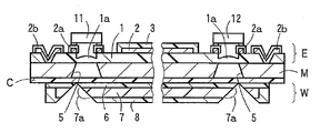
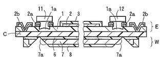
절연층(1)의 표면에 전기 배선(2)이 형성되어 이루어지는 전기 회로 기판(E)과, 이 전기 회로 기판(E)의 전기 배선 형성면에 실장된 광학 소자[발광 소자(11), 수광 소자(12)]와, 상기 전기 회로 기판(E)의 상기 절연층(1)의 이면측에 형성된 광도파로(W)를 구비하고, 그 광도파로(W)의 코어(7)의 단부에, 광(L)을 반사하여 상기 코어(7)와 상기 광학 소자 사이의 광 전파를 가능하게 하는 반사면(7a)이 형성된 광전기 혼재 기판으로서, 상기 절연층(1)이 투광성 재료로 이루어지고, 상기 코어(7)에 형성된 상기 반사면(7a)과 상기 광학 소자 사이의 광로에 대응하는 상기 절연층(1)의 부분이 렌즈부(1a)로 형성되어 있다.
Description
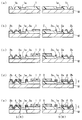
도 2의 (a)∼(d)는 상기 광전기 혼재 기판의 전기 회로 기판의 제작 공정을 모식적으로 도시하는 설명도이며, (e)는 상기 광전기 혼재 기판의 금속층의 에칭 공정을 모식적으로 도시하는 설명도이다.
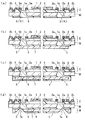
도 3의 (a)∼(d)는 상기 광전기 혼재 기판의 광도파로의 제작 공정을 모식적으로 도시하는 설명도이다.
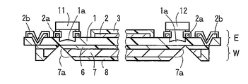
도 4는 본 발명의 광전기 혼재 기판의 제2 실시형태를 모식적으로 도시하는 종단면도이다.
도 5는 본 발명의 광전기 혼재 기판의 제3 실시형태를 모식적으로 도시하는 종단면도이다.
도 6은 본 발명의 광전기 혼재 기판의 제4 실시형태를 모식적으로 도시하는 종단면도이다.
도 7은 종래의 광전기 혼재 기판을 모식적으로 도시하는 종단면도이다.
도 8은 종래의 광 배선 기판을 모식적으로 도시하는 종단면도이다.

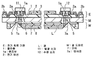
L: 광 1: 절연층
1a: 렌즈부 2: 전기 배선
7: 코어 7a: 반사면
11: 발광 소자 12: 수광 소자
Claims (6)
- 절연층의 표면에 전기 배선이 형성되어 이루어지는 전기 회로 기판과, 이 전기 회로 기판의 전기 배선 형성면에 실장된 광학 소자와, 상기 전기 회로 기판의 상기 절연층의 이면측에 형성된 광도파로를 구비하고, 그 광도파로의 코어의 단부에, 광을 반사하여 상기 코어와 상기 광학 소자 사이의 광 전파를 가능하게 하는 반사부가 형성된 광전기 혼재 기판으로서,
상기 절연층은 투광성 재료로 이루어지고, 상기 코어에 형성된 상기 반사부와 상기 광학 소자 사이의 광로에 대응하는 상기 절연층의 부분은 렌즈부로 형성되어 있는 것을 특징으로 하는 광전기 혼재 기판. - 제1항에 있어서, 상기 절연층의 투광성 재료는 감광성 수지이고, 상기 렌즈부는 포토리소그래피법일 때의 계조 노광에 의해 형성된 것인 광전기 혼재 기판.
- 제1항 또는 제2항에 있어서, 상기 절연층에, 상기 전기 배선의 위치 결정용 얼라인먼트 마크가 형성되고, 상기 전기 배선은 상기 얼라인먼트 마크를 안표로 하여 형성되어 있는 것인 광전기 혼재 기판.
- 제1항 또는 제2항에 있어서, 상기 절연층에, 상기 광학 소자의 위치 결정용 얼라인먼트 마크가 형성되고, 상기 광학 소자는 상기 얼라인먼트 마크를 안표로 하여 실장되어 있는 것인 광전기 혼재 기판.
- 제1항 또는 제2항에 있어서, 상기 절연층은 파장 600 ㎚ 이상의 광의 투과율이 70% 이상인 것인 광전기 혼재 기판.
- 제1항 또는 제2항에 있어서, 상기 절연층은 150℃ 이상의 내열성을 갖는 내열층인 것인 광전기 혼재 기판.
Applications Claiming Priority (2)
| Application Number | Priority Date | Filing Date | Title |
|---|---|---|---|
| JP2012077272A JP5877749B2 (ja) | 2012-03-29 | 2012-03-29 | 光電気混載基板の製法 |
| JPJP-P-2012-077272 | 2012-03-29 |
Publications (2)
| Publication Number | Publication Date |
|---|---|
| KR20130111280A true KR20130111280A (ko) | 2013-10-10 |
| KR102094552B1 KR102094552B1 (ko) | 2020-03-27 |
Family
ID=47884156
Family Applications (1)
| Application Number | Title | Priority Date | Filing Date |
|---|---|---|---|
| KR1020130022798A Expired - Fee Related KR102094552B1 (ko) | 2012-03-29 | 2013-03-04 | 광전기 혼재 기판 |
Country Status (6)
| Country | Link |
|---|---|
| US (1) | US9335497B2 (ko) |
| EP (1) | EP2645142A1 (ko) |
| JP (1) | JP5877749B2 (ko) |
| KR (1) | KR102094552B1 (ko) |
| CN (1) | CN103364893A (ko) |
| TW (1) | TWI578040B (ko) |
Cited By (3)
| Publication number | Priority date | Publication date | Assignee | Title |
|---|---|---|---|---|
| KR20170076655A (ko) * | 2014-10-24 | 2017-07-04 | 닛토덴코 가부시키가이샤 | 광전기 혼재 기판 및 그 제법 |
| KR20170076685A (ko) * | 2014-10-28 | 2017-07-04 | 닛토덴코 가부시키가이샤 | 광전기 혼재 기판 |
| WO2024058376A1 (ko) * | 2022-09-16 | 2024-03-21 | 주식회사 엘지에너지솔루션 | 컨포멀 코팅층을 광 도파로로 이용하는 광 통신 장치 |
Families Citing this family (19)
| Publication number | Priority date | Publication date | Assignee | Title |
|---|---|---|---|---|
| US9023274B2 (en) | 2012-01-31 | 2015-05-05 | Surfacide, Llc | Hard surface disinfection system and method |
| JP2014041181A (ja) * | 2012-08-21 | 2014-03-06 | Hitachi Chemical Co Ltd | レンズ付き基板及びその製造方法、並びにレンズ付き光導波路 |
| JP2014238491A (ja) * | 2013-06-07 | 2014-12-18 | 日東電工株式会社 | 光電気混載モジュール |
| TW201506481A (zh) | 2013-07-02 | 2015-02-16 | Sumitomo Bakelite Co | 光模組用構件、光模組及電子機器 |
| JP6319762B2 (ja) * | 2013-10-31 | 2018-05-09 | 日東電工株式会社 | 光電気混載基板およびその製法 |
| CN103763855B (zh) * | 2014-01-28 | 2016-08-24 | 华进半导体封装先导技术研发中心有限公司 | 光电印制板及其制作方法 |
| US9829663B2 (en) * | 2014-02-25 | 2017-11-28 | Empire Technology Development Llc | Silicon chip with refractive index gradient for optical communication |
| JP6525240B2 (ja) * | 2014-10-24 | 2019-06-05 | 日東電工株式会社 | 光電気混載基板およびその製法 |
| CN105629401A (zh) * | 2014-10-28 | 2016-06-01 | 富士康(昆山)电脑接插件有限公司 | 光电转换装置 |
| JP6674691B2 (ja) * | 2014-12-10 | 2020-04-01 | 日東電工株式会社 | 光電気混載基板 |
| CN104777564B (zh) * | 2015-04-24 | 2017-08-11 | 华进半导体封装先导技术研发中心有限公司 | 一种芯片载板及其制备方法 |
| CN104793288A (zh) * | 2015-04-30 | 2015-07-22 | 上海美维科技有限公司 | 一种含有光波导耦合器件的印制线路板的制造方法 |
| JP6623344B2 (ja) | 2016-03-22 | 2019-12-25 | 日東電工株式会社 | 光導波路積層体およびその製法 |
| JP6713922B2 (ja) * | 2016-12-21 | 2020-06-24 | 日本特殊陶業株式会社 | 光学素子搭載用配線基板 |
| US10025044B1 (en) * | 2017-01-17 | 2018-07-17 | International Business Machines Corporation | Optical structure |
| CN113692106B (zh) * | 2020-05-17 | 2026-02-13 | 合圣科技股份有限公司 | 混合多层光学可挠曲印刷电路组件以及其制造方法 |
| US12366715B2 (en) * | 2020-07-29 | 2025-07-22 | Nitto Denko Corporation | Opto-electric hybrid board |
| JP2022026578A (ja) * | 2020-07-31 | 2022-02-10 | 日東電工株式会社 | 光電気混載基板 |
| US11768338B2 (en) * | 2021-05-27 | 2023-09-26 | Taiwan Semiconductor Manufacturing Company, Ltd. | Optical interconnect structure, package structure and fabricating method thereof |
Citations (5)
| Publication number | Priority date | Publication date | Assignee | Title |
|---|---|---|---|---|
| JP2002258081A (ja) | 2001-02-28 | 2002-09-11 | Fujitsu Ltd | 光配線基板、光配線基板の製造方法及び多層光配線 |
| JP2003255166A (ja) * | 2002-02-28 | 2003-09-10 | Matsushita Electric Ind Co Ltd | 立体光導波路、その製造方法、光モジュール、および光伝送システム |
| JP2004361858A (ja) * | 2003-06-06 | 2004-12-24 | Sharp Corp | マイクロレンズ付き光導波路およびその製造方法 |
| KR20090112585A (ko) * | 2008-04-24 | 2009-10-28 | 닛토덴코 가부시키가이샤 | 광전기 혼재 기판의 제조 방법 |
| JP2009288341A (ja) | 2008-05-27 | 2009-12-10 | Nitto Denko Corp | 光電気混載モジュールおよびその製造方法 |
Family Cites Families (15)
| Publication number | Priority date | Publication date | Assignee | Title |
|---|---|---|---|---|
| US5101454A (en) * | 1991-02-20 | 1992-03-31 | At&T Bell Laboratories | Light emitting diode with multifaceted reflector to increase coupling efficiency and alignment tolerance |
| JP2002189137A (ja) * | 2000-12-20 | 2002-07-05 | Nippon Telegr & Teleph Corp <Ntt> | 光配線基板 |
| JP2004302188A (ja) * | 2003-03-31 | 2004-10-28 | Hitachi Cable Ltd | 光導波路付き電気配線基板 |
| KR100558438B1 (ko) * | 2003-06-25 | 2006-03-10 | 삼성전기주식회사 | 광 스위치의 제조 방법 |
| JP2005017678A (ja) * | 2003-06-26 | 2005-01-20 | Ricoh Co Ltd | 光半導体装置および光半導体装置の製造方法および光半導体システムおよび光半導体システムの製造方法および光インターコネクションモジュール |
| JP2005181645A (ja) * | 2003-12-19 | 2005-07-07 | Sony Corp | 光導波路及びその製造方法、並びに光情報処理装置 |
| JP2006038958A (ja) * | 2004-07-22 | 2006-02-09 | Sharp Corp | 集光素子、その製造方法、光電気配線基板およびその製造方法 |
| JP2006052992A (ja) * | 2004-08-10 | 2006-02-23 | Fuji Xerox Co Ltd | 光導波路配線基板又は光電気混載基板の検査方法 |
| JP2006208527A (ja) * | 2005-01-26 | 2006-08-10 | Fuji Xerox Co Ltd | 光導波路を備えた回路モジュール及びその製造方法 |
| WO2009098834A1 (ja) * | 2008-02-08 | 2009-08-13 | Hitachi Chemical Company, Ltd. | 光配線プリント基板の製造方法および光配線プリント回路基板 |
| JP2010204504A (ja) * | 2009-03-05 | 2010-09-16 | Sekisui Chem Co Ltd | 成形型を作製するためのエッチング用マスクの製造方法及び成形型の製造方法 |
| JP2011081071A (ja) * | 2009-10-05 | 2011-04-21 | Hitachi Cable Ltd | 光モジュール |
| JP5853351B2 (ja) * | 2010-03-25 | 2016-02-09 | ソニー株式会社 | 半導体装置、半導体装置の製造方法、及び電子機器 |
| JP5278366B2 (ja) * | 2010-04-06 | 2013-09-04 | 住友ベークライト株式会社 | 光導波路構造体および電子機器 |
| JP2012037818A (ja) * | 2010-08-11 | 2012-02-23 | Hitachi Ltd | 光電気複合配線モジュールおよびその製造方法 |
-
2012
- 2012-03-29 JP JP2012077272A patent/JP5877749B2/ja active Active
-
2013
- 2013-03-04 CN CN2013100668456A patent/CN103364893A/zh active Pending
- 2013-03-04 KR KR1020130022798A patent/KR102094552B1/ko not_active Expired - Fee Related
- 2013-03-04 EP EP13157566.4A patent/EP2645142A1/en not_active Withdrawn
- 2013-03-04 TW TW102107502A patent/TWI578040B/zh not_active IP Right Cessation
- 2013-03-05 US US13/785,553 patent/US9335497B2/en active Active
Patent Citations (5)
| Publication number | Priority date | Publication date | Assignee | Title |
|---|---|---|---|---|
| JP2002258081A (ja) | 2001-02-28 | 2002-09-11 | Fujitsu Ltd | 光配線基板、光配線基板の製造方法及び多層光配線 |
| JP2003255166A (ja) * | 2002-02-28 | 2003-09-10 | Matsushita Electric Ind Co Ltd | 立体光導波路、その製造方法、光モジュール、および光伝送システム |
| JP2004361858A (ja) * | 2003-06-06 | 2004-12-24 | Sharp Corp | マイクロレンズ付き光導波路およびその製造方法 |
| KR20090112585A (ko) * | 2008-04-24 | 2009-10-28 | 닛토덴코 가부시키가이샤 | 광전기 혼재 기판의 제조 방법 |
| JP2009288341A (ja) | 2008-05-27 | 2009-12-10 | Nitto Denko Corp | 光電気混載モジュールおよびその製造方法 |
Cited By (3)
| Publication number | Priority date | Publication date | Assignee | Title |
|---|---|---|---|---|
| KR20170076655A (ko) * | 2014-10-24 | 2017-07-04 | 닛토덴코 가부시키가이샤 | 광전기 혼재 기판 및 그 제법 |
| KR20170076685A (ko) * | 2014-10-28 | 2017-07-04 | 닛토덴코 가부시키가이샤 | 광전기 혼재 기판 |
| WO2024058376A1 (ko) * | 2022-09-16 | 2024-03-21 | 주식회사 엘지에너지솔루션 | 컨포멀 코팅층을 광 도파로로 이용하는 광 통신 장치 |
Also Published As
| Publication number | Publication date |
|---|---|
| TW201400896A (zh) | 2014-01-01 |
| JP2013205767A (ja) | 2013-10-07 |
| KR102094552B1 (ko) | 2020-03-27 |
| US9335497B2 (en) | 2016-05-10 |
| CN103364893A (zh) | 2013-10-23 |
| JP5877749B2 (ja) | 2016-03-08 |
| TWI578040B (zh) | 2017-04-11 |
| EP2645142A1 (en) | 2013-10-02 |
| US20130259430A1 (en) | 2013-10-03 |
Similar Documents
| Publication | Publication Date | Title |
|---|---|---|
| KR102094552B1 (ko) | 광전기 혼재 기판 | |
| KR102576475B1 (ko) | 광 전기 혼재 기판 | |
| JP6202566B2 (ja) | 光電気混載基板およびその製法 | |
| KR101560407B1 (ko) | 광전기 혼재 모듈과 그 제조 방법 | |
| KR102116143B1 (ko) | 광전기 혼재 기판 및 그 제조 방법 | |
| CN101726794B (zh) | 光电混合组件的制造方法和由该方法获得的光电混合组件 | |
| KR102012050B1 (ko) | 광전기 혼재 기판 및 그 제조 방법 | |
| JP5014855B2 (ja) | 光電気集積配線基板およびその製造方法並びに光電気集積配線システム | |
| KR102523319B1 (ko) | 광전기 혼재 기판 및 그 제법 | |
| JP6525240B2 (ja) | 光電気混載基板およびその製法 | |
| KR102552544B1 (ko) | 광전기 혼재 기판 및 그 제법 | |
| TWI519220B (zh) | 光學印刷電路板及其製造方法 | |
| KR100871252B1 (ko) | 광섬유를 이용한 광/전기 배선을 갖는 연성 인쇄회로기판 | |
| KR20170076685A (ko) | 광전기 혼재 기판 | |
| JP2005099521A (ja) | 光伝送装置 |
Legal Events
| Date | Code | Title | Description |
|---|---|---|---|
| PA0109 | Patent application |
St.27 status event code: A-0-1-A10-A12-nap-PA0109 |
|
| PG1501 | Laying open of application |
St.27 status event code: A-1-1-Q10-Q12-nap-PG1501 |
|
| R17-X000 | Change to representative recorded |
St.27 status event code: A-3-3-R10-R17-oth-X000 |
|
| A201 | Request for examination | ||
| PA0201 | Request for examination |
St.27 status event code: A-1-2-D10-D11-exm-PA0201 |
|
| R17-X000 | Change to representative recorded |
St.27 status event code: A-3-3-R10-R17-oth-X000 |
|
| D13-X000 | Search requested |
St.27 status event code: A-1-2-D10-D13-srh-X000 |
|
| D14-X000 | Search report completed |
St.27 status event code: A-1-2-D10-D14-srh-X000 |
|
| E902 | Notification of reason for refusal | ||
| PE0902 | Notice of grounds for rejection |
St.27 status event code: A-1-2-D10-D21-exm-PE0902 |
|
| P11-X000 | Amendment of application requested |
St.27 status event code: A-2-2-P10-P11-nap-X000 |
|
| P13-X000 | Application amended |
St.27 status event code: A-2-2-P10-P13-nap-X000 |
|
| E90F | Notification of reason for final refusal | ||
| PE0902 | Notice of grounds for rejection |
St.27 status event code: A-1-2-D10-D21-exm-PE0902 |
|
| P11-X000 | Amendment of application requested |
St.27 status event code: A-2-2-P10-P11-nap-X000 |
|
| P13-X000 | Application amended |
St.27 status event code: A-2-2-P10-P13-nap-X000 |
|
| E701 | Decision to grant or registration of patent right | ||
| PE0701 | Decision of registration |
St.27 status event code: A-1-2-D10-D22-exm-PE0701 |
|
| GRNT | Written decision to grant | ||
| PR0701 | Registration of establishment |
St.27 status event code: A-2-4-F10-F11-exm-PR0701 |
|
| PR1002 | Payment of registration fee |
St.27 status event code: A-2-2-U10-U11-oth-PR1002 Fee payment year number: 1 |
|
| PG1601 | Publication of registration |
St.27 status event code: A-4-4-Q10-Q13-nap-PG1601 |
|
| PR1001 | Payment of annual fee |
St.27 status event code: A-4-4-U10-U11-oth-PR1001 Fee payment year number: 4 |
|
| PR1001 | Payment of annual fee |
St.27 status event code: A-4-4-U10-U11-oth-PR1001 Fee payment year number: 5 |
|
| R18-X000 | Changes to party contact information recorded |
St.27 status event code: A-5-5-R10-R18-oth-X000 |
|
| R18-X000 | Changes to party contact information recorded |
St.27 status event code: A-5-5-R10-R18-oth-X000 |
|
| PC1903 | Unpaid annual fee |
St.27 status event code: A-4-4-U10-U13-oth-PC1903 Not in force date: 20250324 Payment event data comment text: Termination Category : DEFAULT_OF_REGISTRATION_FEE |
|
| H13 | Ip right lapsed |
Free format text: ST27 STATUS EVENT CODE: N-4-6-H10-H13-OTH-PC1903 (AS PROVIDED BY THE NATIONAL OFFICE); TERMINATION CATEGORY : DEFAULT_OF_REGISTRATION_FEE Effective date: 20250324 |
|
| PC1903 | Unpaid annual fee |
St.27 status event code: N-4-6-H10-H13-oth-PC1903 Ip right cessation event data comment text: Termination Category : DEFAULT_OF_REGISTRATION_FEE Not in force date: 20250324 |