EP2645570A1 - Optischer bewegungssensor - Google Patents
Optischer bewegungssensor Download PDFInfo
- Publication number
- EP2645570A1 EP2645570A1 EP11843059.4A EP11843059A EP2645570A1 EP 2645570 A1 EP2645570 A1 EP 2645570A1 EP 11843059 A EP11843059 A EP 11843059A EP 2645570 A1 EP2645570 A1 EP 2645570A1
- Authority
- EP
- European Patent Office
- Prior art keywords
- circuit
- photodetector
- motion sensor
- transistor
- voltage
- Prior art date
- Legal status (The legal status is an assumption and is not a legal conclusion. Google has not performed a legal analysis and makes no representation as to the accuracy of the status listed.)
- Withdrawn
Links
Images




Classifications
-
- H—ELECTRICITY
- H03—ELECTRONIC CIRCUITRY
- H03K—PULSE TECHNIQUE
- H03K17/00—Electronic switching or gating, i.e. not by contact-making and –breaking
- H03K17/94—Electronic switching or gating, i.e. not by contact-making and –breaking characterised by the way in which the control signals are generated
- H03K17/945—Proximity switches
-
- H—ELECTRICITY
- H03—ELECTRONIC CIRCUITRY
- H03K—PULSE TECHNIQUE
- H03K17/00—Electronic switching or gating, i.e. not by contact-making and –breaking
- H03K17/94—Electronic switching or gating, i.e. not by contact-making and –breaking characterised by the way in which the control signals are generated
- H03K17/941—Electronic switching or gating, i.e. not by contact-making and –breaking characterised by the way in which the control signals are generated using an optical detector
-
- H—ELECTRICITY
- H03—ELECTRONIC CIRCUITRY
- H03K—PULSE TECHNIQUE
- H03K17/00—Electronic switching or gating, i.e. not by contact-making and –breaking
- H03K17/51—Electronic switching or gating, i.e. not by contact-making and –breaking characterised by the components used
- H03K17/78—Electronic switching or gating, i.e. not by contact-making and –breaking characterised by the components used using opto-electronic devices, i.e. light-emitting and photoelectric devices electrically- or optically-coupled
-
- H—ELECTRICITY
- H03—ELECTRONIC CIRCUITRY
- H03K—PULSE TECHNIQUE
- H03K2217/00—Indexing scheme related to electronic switching or gating, i.e. not by contact-making or -breaking covered by H03K17/00
- H03K2217/94—Indexing scheme related to electronic switching or gating, i.e. not by contact-making or -breaking covered by H03K17/00 characterised by the way in which the control signal is generated
- H03K2217/941—Indexing scheme related to electronic switching or gating, i.e. not by contact-making or -breaking covered by H03K17/00 characterised by the way in which the control signal is generated using an optical detector
- H03K2217/94102—Indexing scheme related to electronic switching or gating, i.e. not by contact-making or -breaking covered by H03K17/00 characterised by the way in which the control signal is generated using an optical detector characterised by the type of activation
- H03K2217/94106—Passive activation of light sensor, e.g. by ambient light
Definitions
- the present invention relates to an optical motion sensor for detecting the existence of a motion in front of the sensor by means of a photodetector.
- KOKAI Japanese Unexamined Patent Application
- No. 10-27451 Patent Literature 1 proposes a stationary detector unit which can detect not only the movement of an object but also the moving direction thereof in a wide range.
- KOKAI Japanese Unexamined Patent Application
- No. 11-186971 Patent Literature 2 proposes an optical receiver in which a plurality of amplifier devices having different amplitude factors are provided in the optical receiver, and the intensity of light received by a photodetector is detected by an intensity monitoring device, whereby the amplifier devices are switched according to the intensity of light received by the photodetector so as not to reduce the light sensitivity while maintaining the dynamic range.
- photodetectors such as photodiodes are small in size, light in weight and inexpensive in price
- photodetectors are incorporated in domestic interior ornament for use as sensors for detecting the movement of a person within a room so that those domestic interior ornaments are activated when the movement of a person is detected thereby.
- the illuminance of the environment where the appliance is placed tends to range from several tens to hundreds of lux. Additionally, the illuminance of a place by a window in the daytime reaches 2000 lux or more from time to time.
- the detection sensitivity of a photodetector is set based on the brightness of a room where no sunlight enters in the daytime, the detection value of a sensor reaches a saturation state when sunlight enters a room where the sensor is placed, it becomes impossible to detect the movement of a person, for example.
- the detection sensitivity of the photodetector is set so as to be applicable to a bright room by taking sunlight into consideration, the detection sensitivity of the sensor is reduced in the room at night, and there have been situations in which the proper operation of the sensor is not ensured.
- a plurality of amplifier circuits having different amplitude factors are incorporated in a sensor by taking into consideration a difference in illuminance between day and night so that the amplifier circuits can be switched depending upon the illuminance detected to ensure the detection sensitivity of the sensor, there is provided a drawback that the circuit configuration of the sensor becomes complex as a motion sensor that is incorporated in a simple interior appliance to detect the movement of a person.
- the invention has been made to eliminate the drawbacks inherent in the related art and an object thereof is to provide a small optical motion sensor with relatively simple circuit configuration that is suitable for incorporation in an interior appliance and which can detect the movement of a person easily and in an ensured fashion throughout the day and night within a room where the illuminance differs totally between day and night.
- an optical motion sensor having a circuit configuration in which a photodetector and a voltage uniforming circuit are connected in series and a connecting point between the photodetector and the voltage uniforming circuit is connected to a signal output terminal via a differential amplifier circuit and a pulse forming circuit.
- the voltage uniforming circuit includes a transistor whose emitter is grounded, a condenser which is inserted between a base and the emitter of the transistor and a resistance which is inserted between the base and a collector of the transistor, and the collector of the transistor is connected to the photodetector.
- the differential amplifier circuit includes a coupling condenser and an inverting amplifier and is configured so that a change in collector potential of the voltage uniforming circuit is inputted into the inverting amplifier via the coupling condenser, whereby the inverting amplifier amplifies the collector potential by an amount corresponding to the change in collector potential for output.
- the pulse forming circuit is desirably a binarizing circuit.
- the photodetector is desirably fixed to near the other end of the cylindrical body which is a different end from the end where the opening portion is provided.
- the photodetector and the voltage uniforming circuit are connected in series, and even though the amount of light entering the photodetector changes moderately and largely, the emitter potential of the photodetector changes small, whereby the proper operation of the photodetector can be maintained whether the optical motion sensor is placed in a bright place or a dimly lit place.
- the voltage uniforming circuit is connected so that the condenser is inserted between the base and the emitter of the transistor whose emitter is grounded, and the resistance is inserted between the base and the collector of the transistor.
- the differential amplifier circuit can easily amplify a change in input potential, and a stable output signal can be formed by the pulse forming circuit having the simple circuit configuration.
- the photodetector is fixed to near the one end of the interior of the cylindrical body to restrict its field of view, it is possible to detect an object moving across the field of view in a more ensured fashion.
- an optical motion sensor uses a phototransistor which is a current-type output photodetector as a photodetector 15.
- the photodetector 15 and a voltage uniforming circuit 21 are disposed in series between power supply terminals so that the phototransistor is inserted between the voltage uniforming circuit 21 and a positive power supply.
- a connecting point between the photodetector 15 and the voltage uniforming circuit 21 is connected to an input terminal of a differential amplifier circuit 31. Then, an output terminal of the differential amplifier circuit 31 is connected to a signal output terminal 39 via a pulse forming circuit 37.
- the photodetector 15 is disposed in a deep portion of a cylindrical body 11, and the photodetector 15 is fixed to near one end of the cylindrical body 11 by a fixing member 13. A distance from the photodetector 15 to an opening portion 17 of the cylindrical body 11 is made several times larger than a bore diameter of the cylindrical body 11.
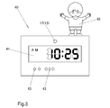
- this optical motion sensor is incorporated, for example, in a clock unit 40 shown in Fig. 3 .
- the clock unit 40 is made into a digital clock and has a plurality of setting switches 43 such as an hour/minute setting switch and an alarm setting switch, accommodating therein the light sensing portion 10 of the optical motion sensor above an hour/minute display portion 41 with the opening portion 17 of the cylindrical body 11 disposed to be exposed to the outside of the clock unit 40.
- the clock unit 40 has a figure which is a movable decorative unit 45.
- the movable decorative unit 45 is configured so as to do such an action as moving a hand or produce a voice or a sound from a speaker when the movement or the like of a person is detected in front of the clock unit 40 by the optical motion sensor.
- a condenser which is a bias condenser 25 is inserted between an emitter and a base of a voltage regulating transistor 23 which is a transistor whose emitter is grounded, and a resistance, which is a regulating resistance 27, is inserted between a collector and the base of the voltage regulating transistor 23.
- the collector of the voltage regulating transistor 23 is connected to an emitter of the phototransistor and is connected to the differential amplifier circuit 31.
- This differential amplifier circuit 31 includes a coupling condenser 33 and an inverting amplifier 35 and inputs an output of the voltage uniforming circuit 21 into the inverting amplifier 35 via the coupling condenser 33.
- the pulse forming circuit 37 uses a binarizing circuit and outputs an on signal of a definite value when an input voltage exceeds a threshold of 1.5V, for example, and outputs an off signal of about 0V when the input voltage is equal to or lower than the threshold.
- the resistance value of the regulating resistance 27 is in the range of hundreds of kilo-ohms to on the order of 1 M ⁇ , and the power supply voltage is 3 V, it is possible to restrain a collector potential of the voltage regulating transistor 23 which is an output voltage of the voltage uniforming circuit 21 from changing from slightly larger than 0.5 V to slightly smaller than 0.7 V, as shown at (2) in Fig. 4 .
- an output current of the photodetector 15 is caused to flow to a negative power supply while dividing it into a resistance current which flows through the regulating resistance 27 and a collector current of the voltage regulating transistor 23, so that the collector potential of the voltage regulating transistor 23 is stabilized to a voltage having a slightly higher value than a potential between the base and the emitter of the voltage regulating transistor 23 which is about 0.5 V.
- the collector potential can be stabilized by keeping small the change in collector potential of the voltage regulating transistor 23.
- this voltage drop corresponds to a voltage drop of zero point several second to on the order of 1 second with the movement of a normal person.
- a voltage corresponding to this voltage fluctuation is inputted into the inverting amplifier 35 via the coupling condenser 33 of the differential amplifier circuit 31, whereby the fluctuating voltage can be amplified to on the order of 2 V as shown at (2) in Fig. 5 .
- a pulse signal having a voltage whose peak value is about 3 V can be formed for output to a signal output terminal 39.
- the threshold of the binarizing circuit is not limited to 1.5 V and hence can be set to 1 V or as required according to the output of the differential amplifier circuit 31 which depends on the photoelectric conversion efficiency of the photodetector 15 or the amplitude factor of the inverting amplifier 35.
- a pulse generating circuit such as a single-shot multivibrator can also be used as the pulse forming circuit 37. Nonetheless, in the event that the binarizing circuit is used as the pulse forming circuit 37, the pulse forming circuit 37 can easily be formed small in size by using a single transistor and several resistances.
- the inverting amplifier 35 of the differential amplifier circuit 31 can also be formed easily by using a single transistor and several resistances or condensers, whereby the small and simple circuit configuration of the differential amplifier circuit 31 can easily be realized.
- the photodetector 15 is disposed in the deep position in the cylindrical body 11 which is situated at the other end thereof which is different from the one end where the opening portion 17 is formed, whereby the range of the field of view of the photodetector 15 is restricted. Because of this, for example, when a person moves across the front of the clock unit 40, in many cases, the whole of the field of view of the photodetector 15 is interrupted completely by part of the body of the person, whereby a change within the field of view is made large to increase the change factor of the amount of light sensed by the photodetector 15, thereby making it possible to detect the movement of a person in a more ensured fashion.
- the optical motion sensor is made up of the voltage uniforming circuit 21, the differential amplifier circuit 31 and the pulse forming circuit 37, which are each formed simple in circuit configuration by using the transistor, and therefore, the optical motion sensor can surely detect the movement of a person with the small and simple circuit even in an environment where the brightness changes largely.
- a control circuit of the movable decorative unit 45 is activated by a pulse signal which is an output signal of the optical motion sensor so as to actuate the movable decorative unit 45 which is a movable portion of the clock unit 40.
- the optical motion sensor according to the invention can detect the movement of a person to thereby form an output signal in an ensured fashion with the small and simple circuit configuration even in the environment where the brightness changes largely, the optical motion sensor can easily be incorporated in an interior ornament which responds to the movement of a person so as to activate the interior ornament.
Landscapes
- Geophysics And Detection Of Objects (AREA)
- Photometry And Measurement Of Optical Pulse Characteristics (AREA)
- Switches Operated By Changes In Physical Conditions (AREA)
- Electronic Switches (AREA)
- Light Receiving Elements (AREA)
- Burglar Alarm Systems (AREA)
Applications Claiming Priority (2)
| Application Number | Priority Date | Filing Date | Title |
|---|---|---|---|
| JP2010263827A JP5185354B2 (ja) | 2010-11-26 | 2010-11-26 | 光学モーションセンサー |
| PCT/JP2011/077870 WO2012070690A1 (ja) | 2010-11-26 | 2011-11-25 | 光学モーションセンサー |
Publications (2)
| Publication Number | Publication Date |
|---|---|
| EP2645570A1 true EP2645570A1 (de) | 2013-10-02 |
| EP2645570A4 EP2645570A4 (de) | 2014-05-07 |
Family
ID=46146022
Family Applications (1)
| Application Number | Title | Priority Date | Filing Date |
|---|---|---|---|
| EP11843059.4A Withdrawn EP2645570A4 (de) | 2010-11-26 | 2011-11-25 | Optischer bewegungssensor |
Country Status (6)
| Country | Link |
|---|---|
| EP (1) | EP2645570A4 (de) |
| JP (1) | JP5185354B2 (de) |
| KR (1) | KR101820194B1 (de) |
| CN (1) | CN103299545A (de) |
| TW (1) | TWI516747B (de) |
| WO (1) | WO2012070690A1 (de) |
Cited By (5)
| Publication number | Priority date | Publication date | Assignee | Title |
|---|---|---|---|---|
| DE102014208386A1 (de) | 2014-05-06 | 2015-11-12 | Robert Bosch Gmbh | Verfahren und Vorrichtung zum Überwachen eines immobilen Raumbereichs |
| US20160267322A1 (en) * | 2015-03-13 | 2016-09-15 | Panasonic Intellectual Property Management Co., Ltd. | Sensor control device, sensor system, and load control system |
| US9869581B2 (en) | 2015-03-13 | 2018-01-16 | Panasonic Intellectual Property Management Co., Ltd. | Detection device, load control device, and load control system |
| US9976895B2 (en) | 2015-03-13 | 2018-05-22 | Panasonic Intellectual Property Management Co., Ltd. | Sensor control device, sensor system, and load control system |
| EP2687813B1 (de) * | 2012-07-18 | 2020-10-28 | Samsung Electronics Co., Ltd | System und Verfahren zur Näherungsdetektion unter Verwendung einer geänderten Lichtmenge des Reflexionslichts |
Families Citing this family (2)
| Publication number | Priority date | Publication date | Assignee | Title |
|---|---|---|---|---|
| KR102136055B1 (ko) | 2014-01-08 | 2020-07-21 | 삼성전자 주식회사 | 오픈-루프 증폭기를 포함하는 비전 센서 칩, 이의 동작 방법, 및 이를 포함하는 데이터 처리 시스템 |
| CN107748359B9 (zh) * | 2017-12-06 | 2024-03-22 | 北醒(北京)光子科技有限公司 | 一种环境光噪声抑制电路及激光雷达 |
Family Cites Families (12)
| Publication number | Priority date | Publication date | Assignee | Title |
|---|---|---|---|---|
| JPH0372793U (de) * | 1989-11-15 | 1991-07-23 | ||
| JPH0583982U (ja) * | 1992-04-15 | 1993-11-12 | 株式会社オーゼン | 物体移動検出装置 |
| JPH07104692A (ja) * | 1992-09-22 | 1995-04-21 | Kokusai Display Kogyo Kk | 人を感知して動作を変える玩具の通電回路 |
| GB2289177B (en) * | 1994-04-29 | 1998-04-15 | Plessey Semiconductors Ltd | Receiver arrangement |
| JPH1027451A (ja) | 1996-07-12 | 1998-01-27 | Sony Corp | 記録媒体収納用キャディ及びこれに使用するディスク状記録媒体 |
| JPH10274517A (ja) | 1997-01-31 | 1998-10-13 | Omron Corp | 検出装置 |
| JPH1188068A (ja) * | 1997-09-12 | 1999-03-30 | Sharp Corp | 受光アンプ回路 |
| JP3437917B2 (ja) * | 1997-09-26 | 2003-08-18 | シャープ株式会社 | 受光増幅装置 |
| JP3820718B2 (ja) * | 1997-12-19 | 2006-09-13 | 住友電気工業株式会社 | 光受信器 |
| JP3072793U (ja) * | 2000-03-06 | 2000-11-02 | 株式会社エスティイー | クリスマスツリー |
| US7358819B2 (en) * | 2006-01-17 | 2008-04-15 | Rockwell Automation Technologies, Inc. | Reduced-size sensor circuit |
| JP5320841B2 (ja) * | 2008-06-17 | 2013-10-23 | 住友電気工業株式会社 | 増幅器および光モジュール |
-
2010
- 2010-11-26 JP JP2010263827A patent/JP5185354B2/ja active Active
-
2011
- 2011-11-25 KR KR1020137016510A patent/KR101820194B1/ko not_active Expired - Fee Related
- 2011-11-25 WO PCT/JP2011/077870 patent/WO2012070690A1/ja not_active Ceased
- 2011-11-25 CN CN2011800569360A patent/CN103299545A/zh active Pending
- 2011-11-25 EP EP11843059.4A patent/EP2645570A4/de not_active Withdrawn
- 2011-11-25 TW TW100143265A patent/TWI516747B/zh not_active IP Right Cessation
Cited By (6)
| Publication number | Priority date | Publication date | Assignee | Title |
|---|---|---|---|---|
| EP2687813B1 (de) * | 2012-07-18 | 2020-10-28 | Samsung Electronics Co., Ltd | System und Verfahren zur Näherungsdetektion unter Verwendung einer geänderten Lichtmenge des Reflexionslichts |
| DE102014208386A1 (de) | 2014-05-06 | 2015-11-12 | Robert Bosch Gmbh | Verfahren und Vorrichtung zum Überwachen eines immobilen Raumbereichs |
| US20160267322A1 (en) * | 2015-03-13 | 2016-09-15 | Panasonic Intellectual Property Management Co., Ltd. | Sensor control device, sensor system, and load control system |
| US9792493B2 (en) | 2015-03-13 | 2017-10-17 | Panasonic Intellectual Property Management Co., Ltd. | Sensor control device, sensor system, and load control system |
| US9869581B2 (en) | 2015-03-13 | 2018-01-16 | Panasonic Intellectual Property Management Co., Ltd. | Detection device, load control device, and load control system |
| US9976895B2 (en) | 2015-03-13 | 2018-05-22 | Panasonic Intellectual Property Management Co., Ltd. | Sensor control device, sensor system, and load control system |
Also Published As
| Publication number | Publication date |
|---|---|
| JP5185354B2 (ja) | 2013-04-17 |
| JP2012114812A (ja) | 2012-06-14 |
| KR101820194B1 (ko) | 2018-01-18 |
| TW201224407A (en) | 2012-06-16 |
| KR20130125781A (ko) | 2013-11-19 |
| WO2012070690A1 (ja) | 2012-05-31 |
| TWI516747B (zh) | 2016-01-11 |
| CN103299545A (zh) | 2013-09-11 |
| EP2645570A4 (de) | 2014-05-07 |
Similar Documents
| Publication | Publication Date | Title |
|---|---|---|
| KR101820194B1 (ko) | 광학 모션 센서 | |
| US8288703B2 (en) | Photodetection device | |
| US8629779B2 (en) | Adapting a scanning point of a sample and hold circuit of an optical smoke detector | |
| WO2006057322A1 (en) | Wireless sensor device | |
| TW200503413A (en) | Automatic gain control with two power detectors | |
| JPS5816456B2 (ja) | 光監視装置 | |
| WO2008067157A3 (en) | Automatic discovery and classification of detectors used in unattended ground sensor systems | |
| JP5695338B2 (ja) | 照度センサ | |
| CN112073574A (zh) | 用于感测用户输入的设备 | |
| CN102724796B (zh) | 光控灯具的智能被动感应方法 | |
| CN104062005B (zh) | 受光电路 | |
| JPS57203129A (en) | Light pen and picture processing device using this light pen | |
| US8735826B2 (en) | Human infrared recipient processor | |
| JP2010160750A (ja) | 煙感知器 | |
| US20170005508A1 (en) | Electronic device | |
| US6326622B1 (en) | PIR device | |
| CN105841807A (zh) | 一种提高光传感器检测稳定性的方法、系统及智能终端 | |
| JP2014183383A (ja) | 受光回路 | |
| HK1189303A (en) | Optical motion sensor | |
| EP1418445A3 (de) | Photoelektrischer Sensor | |
| JP5161753B2 (ja) | 煙感知器 | |
| CN109217866A (zh) | 光电开关 | |
| KR101775937B1 (ko) | 개선된 ir 리시버 구조 | |
| CN220673869U (zh) | 传感器电路和电子设备 | |
| JP5227156B2 (ja) | 煙感知器 |
Legal Events
| Date | Code | Title | Description |
|---|---|---|---|
| PUAI | Public reference made under article 153(3) epc to a published international application that has entered the european phase |
Free format text: ORIGINAL CODE: 0009012 |
|
| 17P | Request for examination filed |
Effective date: 20130612 |
|
| AK | Designated contracting states |
Kind code of ref document: A1 Designated state(s): AL AT BE BG CH CY CZ DE DK EE ES FI FR GB GR HR HU IE IS IT LI LT LU LV MC MK MT NL NO PL PT RO RS SE SI SK SM TR |
|
| DAX | Request for extension of the european patent (deleted) | ||
| A4 | Supplementary search report drawn up and despatched |
Effective date: 20140404 |
|
| RIC1 | Information provided on ipc code assigned before grant |
Ipc: H03K 17/78 20060101ALI20140331BHEP Ipc: H03K 17/945 20060101AFI20140331BHEP Ipc: H03K 17/94 20060101ALN20140331BHEP Ipc: H04B 10/114 20130101ALN20140331BHEP Ipc: H03F 3/08 20060101ALN20140331BHEP |
|
| STAA | Information on the status of an ep patent application or granted ep patent |
Free format text: STATUS: THE APPLICATION IS DEEMED TO BE WITHDRAWN |
|
| 18D | Application deemed to be withdrawn |
Effective date: 20141105 |