EP2647038B1 - Structures à nanofils en silicium et en silicium-germanium - Google Patents
Structures à nanofils en silicium et en silicium-germanium Download PDFInfo
- Publication number
- EP2647038B1 EP2647038B1 EP11844167.4A EP11844167A EP2647038B1 EP 2647038 B1 EP2647038 B1 EP 2647038B1 EP 11844167 A EP11844167 A EP 11844167A EP 2647038 B1 EP2647038 B1 EP 2647038B1
- Authority
- EP
- European Patent Office
- Prior art keywords
- silicon
- structures
- nanowire
- substrate
- gate
- Prior art date
- Legal status (The legal status is an assumption and is not a legal conclusion. Google has not performed a legal analysis and makes no representation as to the accuracy of the status listed.)
- Active
Links
Images











Classifications
-
- H—ELECTRICITY
- H10—SEMICONDUCTOR DEVICES; ELECTRIC SOLID-STATE DEVICES NOT OTHERWISE PROVIDED FOR
- H10D—INORGANIC ELECTRIC SEMICONDUCTOR DEVICES
- H10D30/00—Field-effect transistors [FET]
- H10D30/01—Manufacture or treatment
- H10D30/021—Manufacture or treatment of FETs having insulated gates [IGFET]
- H10D30/024—Manufacture or treatment of FETs having insulated gates [IGFET] of fin field-effect transistors [FinFET]
-
- B—PERFORMING OPERATIONS; TRANSPORTING
- B82—NANOTECHNOLOGY
- B82Y—SPECIFIC USES OR APPLICATIONS OF NANOSTRUCTURES; MEASUREMENT OR ANALYSIS OF NANOSTRUCTURES; MANUFACTURE OR TREATMENT OF NANOSTRUCTURES
- B82Y10/00—Nanotechnology for information processing, storage or transmission, e.g. quantum computing or single electron logic
-
- H—ELECTRICITY
- H10—SEMICONDUCTOR DEVICES; ELECTRIC SOLID-STATE DEVICES NOT OTHERWISE PROVIDED FOR
- H10D—INORGANIC ELECTRIC SEMICONDUCTOR DEVICES
- H10D30/00—Field-effect transistors [FET]
- H10D30/01—Manufacture or treatment
- H10D30/014—Manufacture or treatment of FETs having zero-dimensional [0D] or one-dimensional [1D] channels, e.g. quantum wire FETs, single-electron transistors [SET] or Coulomb blockade transistors
-
- H—ELECTRICITY
- H10—SEMICONDUCTOR DEVICES; ELECTRIC SOLID-STATE DEVICES NOT OTHERWISE PROVIDED FOR
- H10D—INORGANIC ELECTRIC SEMICONDUCTOR DEVICES
- H10D30/00—Field-effect transistors [FET]
- H10D30/01—Manufacture or treatment
- H10D30/021—Manufacture or treatment of FETs having insulated gates [IGFET]
- H10D30/031—Manufacture or treatment of FETs having insulated gates [IGFET] of thin-film transistors [TFT]
-
- H—ELECTRICITY
- H10—SEMICONDUCTOR DEVICES; ELECTRIC SOLID-STATE DEVICES NOT OTHERWISE PROVIDED FOR
- H10D—INORGANIC ELECTRIC SEMICONDUCTOR DEVICES
- H10D30/00—Field-effect transistors [FET]
- H10D30/40—FETs having zero-dimensional [0D], one-dimensional [1D] or two-dimensional [2D] charge carrier gas channels
- H10D30/43—FETs having zero-dimensional [0D], one-dimensional [1D] or two-dimensional [2D] charge carrier gas channels having one-dimensional [1D] charge carrier gas channels, e.g. quantum wire FETs or transistors having 1D quantum-confined channels
-
- H—ELECTRICITY
- H10—SEMICONDUCTOR DEVICES; ELECTRIC SOLID-STATE DEVICES NOT OTHERWISE PROVIDED FOR
- H10D—INORGANIC ELECTRIC SEMICONDUCTOR DEVICES
- H10D30/00—Field-effect transistors [FET]
- H10D30/60—Insulated-gate field-effect transistors [IGFET]
- H10D30/62—Fin field-effect transistors [FinFET]
-
- H—ELECTRICITY
- H10—SEMICONDUCTOR DEVICES; ELECTRIC SOLID-STATE DEVICES NOT OTHERWISE PROVIDED FOR
- H10D—INORGANIC ELECTRIC SEMICONDUCTOR DEVICES
- H10D30/00—Field-effect transistors [FET]
- H10D30/60—Insulated-gate field-effect transistors [IGFET]
- H10D30/67—Thin-film transistors [TFT]
- H10D30/6704—Thin-film transistors [TFT] having supplementary regions or layers in the thin films or in the insulated bulk substrates for controlling properties of the device
- H10D30/6713—Thin-film transistors [TFT] having supplementary regions or layers in the thin films or in the insulated bulk substrates for controlling properties of the device characterised by the properties of the source or drain regions, e.g. compositions or sectional shapes
-
- H—ELECTRICITY
- H10—SEMICONDUCTOR DEVICES; ELECTRIC SOLID-STATE DEVICES NOT OTHERWISE PROVIDED FOR
- H10D—INORGANIC ELECTRIC SEMICONDUCTOR DEVICES
- H10D30/00—Field-effect transistors [FET]
- H10D30/60—Insulated-gate field-effect transistors [IGFET]
- H10D30/67—Thin-film transistors [TFT]
- H10D30/6729—Thin-film transistors [TFT] characterised by the electrodes
-
- H—ELECTRICITY
- H10—SEMICONDUCTOR DEVICES; ELECTRIC SOLID-STATE DEVICES NOT OTHERWISE PROVIDED FOR
- H10D—INORGANIC ELECTRIC SEMICONDUCTOR DEVICES
- H10D30/00—Field-effect transistors [FET]
- H10D30/60—Insulated-gate field-effect transistors [IGFET]
- H10D30/67—Thin-film transistors [TFT]
- H10D30/6729—Thin-film transistors [TFT] characterised by the electrodes
- H10D30/673—Thin-film transistors [TFT] characterised by the electrodes characterised by the shapes, relative sizes or dispositions of the gate electrodes
- H10D30/6735—Thin-film transistors [TFT] characterised by the electrodes characterised by the shapes, relative sizes or dispositions of the gate electrodes having gates fully surrounding the channels, e.g. gate-all-around
-
- H—ELECTRICITY
- H10—SEMICONDUCTOR DEVICES; ELECTRIC SOLID-STATE DEVICES NOT OTHERWISE PROVIDED FOR
- H10D—INORGANIC ELECTRIC SEMICONDUCTOR DEVICES
- H10D30/00—Field-effect transistors [FET]
- H10D30/60—Insulated-gate field-effect transistors [IGFET]
- H10D30/67—Thin-film transistors [TFT]
- H10D30/674—Thin-film transistors [TFT] characterised by the active materials
- H10D30/6741—Group IV materials, e.g. germanium or silicon carbide
-
- H—ELECTRICITY
- H10—SEMICONDUCTOR DEVICES; ELECTRIC SOLID-STATE DEVICES NOT OTHERWISE PROVIDED FOR
- H10D—INORGANIC ELECTRIC SEMICONDUCTOR DEVICES
- H10D30/00—Field-effect transistors [FET]
- H10D30/60—Insulated-gate field-effect transistors [IGFET]
- H10D30/67—Thin-film transistors [TFT]
- H10D30/674—Thin-film transistors [TFT] characterised by the active materials
- H10D30/6741—Group IV materials, e.g. germanium or silicon carbide
- H10D30/6743—Silicon
- H10D30/6744—Monocrystalline silicon
-
- H—ELECTRICITY
- H10—SEMICONDUCTOR DEVICES; ELECTRIC SOLID-STATE DEVICES NOT OTHERWISE PROVIDED FOR
- H10D—INORGANIC ELECTRIC SEMICONDUCTOR DEVICES
- H10D30/00—Field-effect transistors [FET]
- H10D30/60—Insulated-gate field-effect transistors [IGFET]
- H10D30/67—Thin-film transistors [TFT]
- H10D30/6757—Thin-film transistors [TFT] characterised by the structure of the channel, e.g. transverse or longitudinal shape or doping profile
-
- H—ELECTRICITY
- H10—SEMICONDUCTOR DEVICES; ELECTRIC SOLID-STATE DEVICES NOT OTHERWISE PROVIDED FOR
- H10D—INORGANIC ELECTRIC SEMICONDUCTOR DEVICES
- H10D30/00—Field-effect transistors [FET]
- H10D30/60—Insulated-gate field-effect transistors [IGFET]
- H10D30/791—Arrangements for exerting mechanical stress on the crystal lattice of the channel regions
- H10D30/797—Arrangements for exerting mechanical stress on the crystal lattice of the channel regions being in source or drain regions, e.g. SiGe source or drain
-
- H—ELECTRICITY
- H10—SEMICONDUCTOR DEVICES; ELECTRIC SOLID-STATE DEVICES NOT OTHERWISE PROVIDED FOR
- H10D—INORGANIC ELECTRIC SEMICONDUCTOR DEVICES
- H10D62/00—Semiconductor bodies, or regions thereof, of devices having potential barriers
- H10D62/10—Shapes, relative sizes or dispositions of the regions of the semiconductor bodies; Shapes of the semiconductor bodies
- H10D62/117—Shapes of semiconductor bodies
- H10D62/118—Nanostructure semiconductor bodies
- H10D62/119—Nanowire, nanosheet or nanotube semiconductor bodies
- H10D62/121—Nanowire, nanosheet or nanotube semiconductor bodies oriented parallel to substrates
-
- H—ELECTRICITY
- H10—SEMICONDUCTOR DEVICES; ELECTRIC SOLID-STATE DEVICES NOT OTHERWISE PROVIDED FOR
- H10D—INORGANIC ELECTRIC SEMICONDUCTOR DEVICES
- H10D62/00—Semiconductor bodies, or regions thereof, of devices having potential barriers
- H10D62/10—Shapes, relative sizes or dispositions of the regions of the semiconductor bodies; Shapes of the semiconductor bodies
- H10D62/117—Shapes of semiconductor bodies
- H10D62/118—Nanostructure semiconductor bodies
- H10D62/119—Nanowire, nanosheet or nanotube semiconductor bodies
- H10D62/122—Nanowire, nanosheet or nanotube semiconductor bodies oriented at angles to substrates, e.g. perpendicular to substrates
-
- H—ELECTRICITY
- H10—SEMICONDUCTOR DEVICES; ELECTRIC SOLID-STATE DEVICES NOT OTHERWISE PROVIDED FOR
- H10D—INORGANIC ELECTRIC SEMICONDUCTOR DEVICES
- H10D62/00—Semiconductor bodies, or regions thereof, of devices having potential barriers
- H10D62/10—Shapes, relative sizes or dispositions of the regions of the semiconductor bodies; Shapes of the semiconductor bodies
- H10D62/13—Semiconductor regions connected to electrodes carrying current to be rectified, amplified or switched, e.g. source or drain regions
- H10D62/149—Source or drain regions of field-effect devices
- H10D62/151—Source or drain regions of field-effect devices of IGFETs
-
- H—ELECTRICITY
- H10—SEMICONDUCTOR DEVICES; ELECTRIC SOLID-STATE DEVICES NOT OTHERWISE PROVIDED FOR
- H10D—INORGANIC ELECTRIC SEMICONDUCTOR DEVICES
- H10D62/00—Semiconductor bodies, or regions thereof, of devices having potential barriers
- H10D62/10—Shapes, relative sizes or dispositions of the regions of the semiconductor bodies; Shapes of the semiconductor bodies
- H10D62/17—Semiconductor regions connected to electrodes not carrying current to be rectified, amplified or switched, e.g. channel regions
- H10D62/213—Channel regions of field-effect devices
- H10D62/221—Channel regions of field-effect devices of FETs
- H10D62/235—Channel regions of field-effect devices of FETs of IGFETs
-
- H—ELECTRICITY
- H10—SEMICONDUCTOR DEVICES; ELECTRIC SOLID-STATE DEVICES NOT OTHERWISE PROVIDED FOR
- H10D—INORGANIC ELECTRIC SEMICONDUCTOR DEVICES
- H10D62/00—Semiconductor bodies, or regions thereof, of devices having potential barriers
- H10D62/80—Semiconductor bodies, or regions thereof, of devices having potential barriers characterised by the materials
- H10D62/82—Heterojunctions
- H10D62/822—Heterojunctions comprising only Group IV materials heterojunctions, e.g. Si/Ge heterojunctions
-
- H—ELECTRICITY
- H10—SEMICONDUCTOR DEVICES; ELECTRIC SOLID-STATE DEVICES NOT OTHERWISE PROVIDED FOR
- H10D—INORGANIC ELECTRIC SEMICONDUCTOR DEVICES
- H10D62/00—Semiconductor bodies, or regions thereof, of devices having potential barriers
- H10D62/80—Semiconductor bodies, or regions thereof, of devices having potential barriers characterised by the materials
- H10D62/83—Semiconductor bodies, or regions thereof, of devices having potential barriers characterised by the materials being Group IV materials, e.g. B-doped Si or undoped Ge
-
- H—ELECTRICITY
- H10—SEMICONDUCTOR DEVICES; ELECTRIC SOLID-STATE DEVICES NOT OTHERWISE PROVIDED FOR
- H10D—INORGANIC ELECTRIC SEMICONDUCTOR DEVICES
- H10D64/00—Electrodes of devices having potential barriers
- H10D64/01—Manufacture or treatment
- H10D64/017—Manufacture or treatment using dummy gates in processes wherein at least parts of the final gates are self-aligned to the dummy gates, i.e. replacement gate processes
-
- H—ELECTRICITY
- H10—SEMICONDUCTOR DEVICES; ELECTRIC SOLID-STATE DEVICES NOT OTHERWISE PROVIDED FOR
- H10D—INORGANIC ELECTRIC SEMICONDUCTOR DEVICES
- H10D84/00—Integrated devices formed in or on semiconductor substrates that comprise only semiconducting layers, e.g. on Si wafers or on GaAs-on-Si wafers
- H10D84/80—Integrated devices formed in or on semiconductor substrates that comprise only semiconducting layers, e.g. on Si wafers or on GaAs-on-Si wafers characterised by the integration of at least one component covered by groups H10D12/00 or H10D30/00, e.g. integration of IGFETs
- H10D84/82—Integrated devices formed in or on semiconductor substrates that comprise only semiconducting layers, e.g. on Si wafers or on GaAs-on-Si wafers characterised by the integration of at least one component covered by groups H10D12/00 or H10D30/00, e.g. integration of IGFETs of only field-effect components
- H10D84/83—Integrated devices formed in or on semiconductor substrates that comprise only semiconducting layers, e.g. on Si wafers or on GaAs-on-Si wafers characterised by the integration of at least one component covered by groups H10D12/00 or H10D30/00, e.g. integration of IGFETs of only field-effect components of only insulated-gate FETs [IGFET]
- H10D84/85—Complementary IGFETs, e.g. CMOS
- H10D84/856—Complementary IGFETs, e.g. CMOS the complementary IGFETs having different architectures than each other, e.g. high-voltage and low-voltage CMOS
-
- H—ELECTRICITY
- H10—SEMICONDUCTOR DEVICES; ELECTRIC SOLID-STATE DEVICES NOT OTHERWISE PROVIDED FOR
- H10D—INORGANIC ELECTRIC SEMICONDUCTOR DEVICES
- H10D86/00—Integrated devices formed in or on insulating or conducting substrates, e.g. formed in silicon-on-insulator [SOI] substrates or on stainless steel or glass substrates
- H10D86/201—Integrated devices formed in or on insulating or conducting substrates, e.g. formed in silicon-on-insulator [SOI] substrates or on stainless steel or glass substrates the substrates comprising an insulating layer on a semiconductor body, e.g. SOI
-
- H—ELECTRICITY
- H10—SEMICONDUCTOR DEVICES; ELECTRIC SOLID-STATE DEVICES NOT OTHERWISE PROVIDED FOR
- H10W—GENERIC PACKAGES, INTERCONNECTIONS, CONNECTORS OR OTHER CONSTRUCTIONAL DETAILS OF DEVICES COVERED BY CLASS H10
- H10W10/00—Isolation regions in semiconductor bodies between components of integrated devices
- H10W10/01—Manufacture or treatment
- H10W10/011—Manufacture or treatment of isolation regions comprising dielectric materials
- H10W10/014—Manufacture or treatment of isolation regions comprising dielectric materials using trench refilling with dielectric materials, e.g. shallow trench isolations
-
- H—ELECTRICITY
- H10—SEMICONDUCTOR DEVICES; ELECTRIC SOLID-STATE DEVICES NOT OTHERWISE PROVIDED FOR
- H10W—GENERIC PACKAGES, INTERCONNECTIONS, CONNECTORS OR OTHER CONSTRUCTIONAL DETAILS OF DEVICES COVERED BY CLASS H10
- H10W10/00—Isolation regions in semiconductor bodies between components of integrated devices
- H10W10/10—Isolation regions comprising dielectric materials
- H10W10/17—Isolation regions comprising dielectric materials formed using trench refilling with dielectric materials, e.g. shallow trench isolations
Definitions
- Nanowires used to fabricate devices provide improved short channel control.
- silicon germanium (Si x Ge 1-x ) nanowire channel structures (where x ⁇ 0.5) provide mobility enhancement at respectable Eg, which is suitable for use in many conventional products which utilize higher voltage operation.
- silicon germanium (Si x Ge 1-x ) nanowire channels (where x>0.5) provide mobility enhanced at lower Egs (suitable for low voltage products in the mobile/handheld domain, for example.
- US 2004/262690 A1 describes a MOS transistor formed in a silicon substrate comprising an active area surrounded with an insulating wall, a first conductive strip covering a central strip of the active area, one or several second conductive strips placed in the active area right above the first strip, and conductive regions placed in two recesses of the insulating wall and placed against the ends of the first and second strips, the silicon surfaces opposite to the conductive strips and regions being covered with an insulator forming a gate oxide.
- US 2008/237575 A1 describes a method to provide a transistor or memory cell structure comprising: providing a substrate including a lower Si substrate and an insulating layer on the substrate; providing a first projection extending above the insulating layer, the first projection including an Si material and a Si 1-x Ge x material; and exposing the first projection to preferential oxidation to yield a second projection including a center region comprising Ge/Si 1-y Ge y and a covering region comprising SiO 2 and enclosing the center region.
- US 2007/017439 A1 describes a method of fabricating nanowires and a method of fabricating a transistor having the same.
- the method includes: forming a template layer on a substrate, the template layer having a first lateral surface and a second lateral surface facing the first surface; forming pores in the template layer, the pores disposed between the first lateral surface and the second lateral surface in the template layer and having first apertures in the first lateral surface; forming a single-crystalline material layer contacting the first apertures disposed in the first lateral surface of the template layer; forming second apertures connecting pores disposed in the second lateral surface; supplying gaseous crystal growth materials through the second apertures; and forming crystalline nanowires in the pores by crystal growth from the single-crystalline material layer.
- US 2006/024874 A1 describes a multi-bridge-channel MOSFET (MBCFET) formed by forming a stacked structure on a substrate that includes channel layers and interchannel layers interposed between the channel layers. Trenches are formed by selectively etching the stacked structure. The trenches run across the stacked structure parallel to each other and separate a first stacked portion including channel patterns and interchannel patterns from second stacked portions including channel and interchannel layers remaining on both sides of the first stacked portion. First source and drain regions are grown using selective epitaxial growth. The first source and drain regions fill the trenches and connect to second source and drain regions defined by the second stacked portions. Marginal sections of the interchannel patterns of the first stacked portion are selectively exposed.
- MBCFET multi-bridge-channel MOSFET
- Through tunnels are formed by selectively removing the interchannel patterns of the first stacked portion beginning with the exposed marginal sections.
- the through tunnels are surrounded by the first source and drain regions and the channel patterns.
- a gate is formed along with a gate dielectric layer, the gate filling the through tunnels and extending onto the first stacked portion.
- US2010295021 discloses a method of manufacturing a nanowire FET comprising a plurality of stacks of nanowires with all-around gates.
- the channel region of a stack of Si and SiGe layers is patterned into a plurality of fins.
- the source drain region is not patterned and partly replaced by a silicide after a replacement gate has been formed around the selectively etched nanowires.
- the present invention relates to a method of forming a portion of a gate-all-around nanowire device according to claim 1.
- Those methods and structures may include forming a nanowire device comprising a substrate comprising source/drain structures comprising nanowires between the source/drain structures, wherein the nanowire channel structures are vertically stacked above each other.
- Various embodiments included herein enable mobility improvement and short channel control as device dimensions scale past the 15nm node. Embodiments further enable enhanced isolation of channels from the substrate, mitigation of the capacitance associated with spacer-gap separation, and vertical architecture scaling with nanowires.
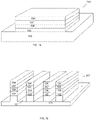
- FIGS. 1a-1n illustrate embodiments of forming microelectronic structures, such as forming nanowire device structures, for example.
- FIG. 1a illustrates a substrate 100.
- the substrate 100 may comprise a bulk silicon substrate 100.
- the substrate 100 may comprise a silicon on insulator substrate (SOI) 100, but may also include any type of suitable substrate material.
- SOI silicon on insulator substrate
- a stack of alternating layers of epitaxial silicon-germanium and silicon is formed.
- a first silicon germanium 102 material may be grown by epitaxial growth on the substrate 100.
- a first silicon material 104 may be epitaxially grown on the epitaxial first silicon germanium 102.
- a second layer of silicon germanium 102' may be formed on the first silicon layer 102, and a second layer of silicon 104' may be formed on the second silicon germanium 102'.
- the numbers of alternating epitaxial silicon germanium layers 102 /epitaxial silicon layers 104 formed on the substrate 100 may be varied, depending upon the particular application. In another embodiment, the layer order can be reversed with alternating layers of epitaxial silicon 104 and epitaxial silicon germanium 102 formed on the substrate 100.
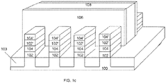
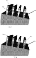
- the epitaxial stack 120 of silicon germanium/silicon/silicon germanium/silicon is patterned to form a plurality of fin structures 107 separated by trenches 101. This may be done using conventional patterning/etching techniques ( FIG. 1b ).
- the stack structure 120 may be etched at a trench etch process, such as during a shallow trench isolation (STI) process, wherein trenches 101 are formed in the substrate 100 to form fin structures 107.
- STI shallow trench isolation
- Each of the fin structures formed 107 may be separated from each other by an oxide 103, that may be formed in the trenches 101.
- the fin structures 107 may comprise a dual channel portion of a gate all around (GAA) nanowire device.
- the number of channels in the device will depend on the numbers of layers in the fin structures 107.
- the fin structures 107 comprise nanowire structures.
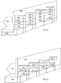
- Spacers 106 are then formed on and across the fin structures 107 and may be disposed orthogonally with respect to the fin structures 107 ( FIG.1c ).
- the spacers 106 may comprise any material that may be selective during process to the fin structure 107 materials.
- a sacrificial gate electrode material 108 is formed within/between spacers 106, around portions of the fin structures 107 located between the spacers 106.
- the gate electrode material may be formed around portions of the fin structures 107, and the spacers 106 formed on either side of the gate.
- the gate 108 may comprise polysilicon, in some cases, and comprises a sacrificial gate structure 108.
- a portion of the fin structure 107 may be removed from the substrate 100 to expose source/drain regions 109 ( FIG. 1d ).
- the portion of the fin structure 107 may be etched by a dry etch process to expose the source/drain regions 109.
- the source/drain regions 109 may be etched to terminate on either the substrate 100 or the bottom wire (102 or 104).
- Optional undercut wet or dry etch processes can be utilized to remove additional materials in gate 108 region /tip overlap area depending upon the particular device needs.
- silicon or silicon germanium source drain structures 110 may be grown utilizing epitaxial growth techniques in the source/drain regions 109 ( FIG. 1e ), and may be coupled to the portions of the fin structures 107 disposed between the spacers 106.
- the epitaxial source/drain structures 110 may be n-doped silicon for an NMOS device, or may be p-doped silicon/silicon germanium for a PMOS device, depending on the device type for the particular application. Doping may be introduced in the epitaxial process, by implant, by plasma doping, by solid source doping or by other methods as are known in the art.
- the tip and source/drain junction can be engineered by combining epitaxial layers doped with different dopant species and concentration.
- a silicon etch stop layer/tip 112 may be grown first before the source/drain silicon germanium epitaxial structures 110 are grown, to avoid etching in the source/drain regions 110 during a subsequent silicon germanium etch ( FIG. 1f ).
- the PMOS tip material needs to be resistant to a subsequent silicon germanium etch process.
- An interlayer dielectric may be formed on the substrate 100 (not shown) over the source/drain structures 110 and the gate 108. and spacers 106.
- a top portion of the sacrificial poly gate 108 may be opened by chemical mechanical polish (CMP), in an embodiment.
- CMP chemical mechanical polish
- the sacrificial gate electrode material 108 is then removed from between the spacer materials 106 ( FIG. 1g ).
- FIG. 1h depicts an interior view between the spacers 106, wherein the fin structure 107 is disposed in between the two spacers (only one shown).
- the silicon layers 104, 104' are selectively removed from the fin structure 107 to open up a gap 111 between the silicon germanium channels 102, 102' ( FIG.1i ).
- the silicon layers 104, 104' may be etched selectively with a wet etch that selectively removes the silicon 104, 104' while not etching the silicon germanium nanowire structures 102, 102'.
- Such etch chemistries as aqueous hydroxide chemistries, including ammonium hydroxide and potassium hydroxide, for example, may be utilized to selectively etch the silicon.
- the silicon germanium layers 102, 102' are selectively removed from the fin structure 107 and from sidewalls to open a gap 113 between the silicon channel layers 104, 104' ( FIG. 1j ).
- the silicon germanium 102, 102' may be etched selectively with a wet etch that selectively removes the silicon germanium while not etching the silicon nanowire channels 104, 104'.Such etch chemistries as carboxylic acid/nitric acid/HF chemistry, and citric acid/nitric acid/HF, for example, may be utilized to selectively etch the silicon germanium.
- either the silicon layers are be removed from the fin structure 107 to form silicon germanium nanowires 102,102', or the silicon germanium layer are removed from the fin structure 107 to form silicon channel nanowire 104, 104' structures in the channel region between the spacers 106.
- Both silicon and silicon germanium channel material may exist on the same wafer, in the same die, or on the same circuit, for example as NMOS Si and PMOS SiGe in an inverter structure.
- the Si channel thickness (SiGe interlayer) and SiGe channel thickness (Si interlayer) may be mutually chosen to enhance circuit performance and/or circuit minimum operating voltage
- the number of wires on different devices in the same circuit may be changed through an etch process to enhance circuit performance and/or circuit minimum operating voltage.
- a gate dielectric material 115 is be formed to surround the channel region between the spacers 106.
- the gate dielectric material 115 may comprise a high k gate electrode material, wherein the dielectric constant may comprise a value greater than about 4.
- the gate dielectric material 115 may be formed conformally all around the silicon nanowire structures 104, 104' between the spacers 106 ( FIG.1k ).
- the gate electrode material 115 may be formed all around silicon germanium nanowire structures 102, 102' in between the spacers 106 (not shown).
- a gate electrode material 117 is then formed around the gate dielectric material 115 (FIG. 11).
- the gate electrode material 117 may comprise metal gate electrode materials such as pure metal and alloys of Ti, W, Ta, Al, including nitrides such as TaN, TiN, and also including alloys with rare earths, such as Er, Dy or noble metals such as Pt.
- the gap 113 between the silicon nanowire structures 104, 104' is filled with the gate electrode material or the gap 111 between the silicon germanium nanowire structures 102, 102' is filled with the gate electrode material 117 (not shown).
- standard CMOS processing may be further performed on the substrate 100 to fabricate a CMOS device according to embodiments herein.
- an NMOS and/or a PMOS device may be formed.
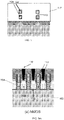
- Figure 1m depicts an NMOS device that may be formed (depicting a single silicon channel), wherein a trench contact 119 couples to the source drain structure 110, which may be silicon doped n+ in some cases, depending upon the particular application.
- the gate electrode material 117 may surround the silicon nanowire channel 104.
- Figure 1n depicts a PMOS device (depicting a single silicon channel 104) wherein a trench contact 119 couples to the source drain structure 110, which may be silicon germanium doped p+ in some cases, depending upon the particular application.
- a silicon epitaxial tip/etch stop 120 which may be p- doped in some cases, may be disposed between the source drain structure 110 and the substrate 100.
- the gate electrode material 117 may surround the silicon channel 104, which may comprise a strained silicon channel 104 in some cases.
- a device utilizing silicon germnaium channel structures may have an advantage by comprising a high carrier mobility due to the silicon germanium properties.
- the gate all around silicon germanium channel device process may be similar to the gate all around silicon channel device processing, except that the epitaxial layer stack 120 may be reversed, that is the silicon material 104 will be formed on the substrate initially, and the silicon germanium formed on the silicon. Since the silicon underlayer will be removed selective to the silicon germanium, the source/drain may comprise silicon germanium, and the etch stop under the sacrificial gate electrode material may comprise silicon germanium as well to avoid substrate etching.
- Embodiments herein enable the fabrication of self-aligned gate-all-around (GAA) silicon and silicon germanium channel transistor structures and devices.
- Nanowire channel devices exhibit lower sub-threshold leakage due to short channel effect (SCE) reduction.
- SCE short channel effect
- GAA SiGe high mobility channel device for example suppress SCE effects.
- (GAA) devices can maximize the electrostatic gate control to the channel.
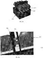
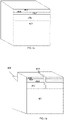
- a bottom nanowire channel 202 that is disposed on a substrate 200 may comprise a shorted trigate with poor subfin leakage, in some instances.
- One solution may comprise forming the device on a silicon on insulator (SOI) substrate 201 ( FIGS. 2b-2c ), wherein source/drain structures 210 and nanowire structures 204 are disposed on an insulator material 203, such as an oxide material 203, rather than being disposed on a bulk silicon substrate 200 (as depicted in FIG. 2a ).
- SOI silicon on insulator
- the bottom nanowire 204 geometry can be defined by etching the bottom oxide after a silicon germanium etching of the nanowire fin structure (similar to the nanowire fin structure 107 of FIG. 1b , for example) and before forming the gate electrode material (similar to the gate electrode material 117 of FIG. 1I , for example).
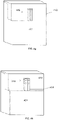
- FIG. 2d depicts etching the dielectric to form one nanowire and one trigate structure
- FIG. 2e depicts etching the dielectric to form a device comprising two nanowires.
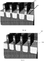
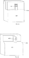
- enhanced substrate isolation may be achieved by forming fin spacers 211 on the fin 207 sidewalls after the trench etch ( FIG. 2f ). Then a second trench etch 214 may be performed to expose a bottom fin area 216, and the silicon portion of the bottom fin area 216 may be oxidized ( FIG.2g ). Thus, a bottom nanowire of the device may be disposed on an oxide to improve substrate isolation.
- fin spacers 211 may be formed on the fin 207 sidewalls after the trench etch and fill ( FIG.
- the bottom silicon portion 216 of the fin 207 may be oxidized after the STI recess formation/oxide fill to enhance substrate isolation ( FIG.2i ).
- a bottom nanowire of the device may be disposed on an oxide to improve substrate isolation.
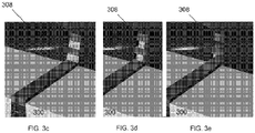
- a gap 311 in a spacer 306 left by the removal of silicon regions of a nanowire stack 307 may be left by the removal of silicon regions of a nanowire stack 307 ( FIG. 3a ).
- a gate such as a metal gate structure (similar to the gate structure 117 of FIG. 1I for example)
- the gap 311 may create a very high-capacitance parasitic region between the subsequently formed gate and the source drain structure 310.
- the potential parasitic region may be avoided by utilizing an epitaxial oxide 302 for the starting stack, rather than silicon (which may or may not require an orientation change on the silicon substrate 300) ( FIG.3b ).
- Alternating layers of an epitaxial semiconductor material 304 may be formed on an epitaxial oxide material 302 that may be formed on the substrate 300.
- a Gd 2 O 3 can be grown epitaxially on (111) silicon, and silicon germanium can then be grown on top of the Gd 2 O 3 to build up a multilayer stack on the substrate that can be etched into fin structures 307, that may be subsequently formed into silicon germanium wires.
- cerium oxide may be grown on (111) silicon (or alternatively on (100) silicon) to form the multilayer stack.
- oxide/semiconductor/oxide stack there is the option to not etch, partially etch, or fully etch the oxide material 302, 302' of the fin structure 307 ( FIGS. 3c-3e , respectively). The no etch option ( FIG.
- the gap 311 in the spacers that is adjacent to the fin structures may be filled with a second spacer 312 comprising spacer-like material 312 or a low-k material 312 from the source/drain 310 side of the spacer 306 prior to epitaxial growth of the source.drain ( FIG. 3f ).
- materials such as but not limited to SiON, SiN, SiC, SiOBN, and low k oxides may comprise the second spacer 312 material.
- all of the silicon in the etch of the stack 307 may be removed, so that the replacement gate etch (removal of the sacrificial gate electrode material) only hits oxide.
- the gap 311 may be filled from the gate side (prior to gate deposition) with a spacer-like material 312 or a low-k material 312 ( FIG.3g ). Examples include performing a full etch or partial etches of the stack 307 (shown as full etch).
- the gap 311 may be filled by exploiting the anisotropy of silicon etches to minimize the etch out of the silicon during the removal step from the stack 307.
- a (110) wafer may be used with a channel along ⁇ 111>. This structure will have slow-etching (111) planes facing the source/drain structures 310, thus limiting undercut.
- the wet etch selected here must also etch SiGe more slowly than Si, leaving a partially etched SiGe nanowire after removing all of the silicon between the SiGe nanowires.
- an anisotropic etch may be used to minimize lateral etching inside the spacer 306, wherein the etch chemistry is highly selective to silicon and not selective to silicon germanium.
- silicon germanium or silicon may be epitaxially grown from a substrate into a trench, and then oxidation or etching processes, for example, may be used to separate fin structures into nanowires, wherein the nanowires may be stacked vertically upon each other.
- oxidation for the entire wire wherein the source/drain region starts out as layers of SiGe (or Si) and oxide) may be performed. Alternating oxide 404 and nitride layers 402 (more layers may be used to form more wires) may be formed on a silicon substrate 401 ( FIG. 4a ).
- the oxide and nitride layers may be patterned and etched to form a trench 405 and a back portion 406, wherein the trench 405 exposes the silicon material of the substrate 401 ( FIG. 4b ).
- Silicon germanium (or silicon) 407 may be grown epitaxially in the trench 405 and back portion, and may be polished ( FIG. 4c ).
- a hard mask 408 may be formed on the silicon germanium (or silicon) 407, and maybe patterned and etched to expose sides of fins 410 ( FIG. 4d ).
- a fin structure may be formed by removing a portion of the alternating layers of nitride and oxide not covered by the hard mask.
- the fins 410 may be oxidized to define nanowires ( FIG. 4e ).
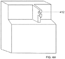
- the oxidized portions of the fins 410 may be removed to form the nanowires 412 which may serve as channel structures for a device, and may be formed across substantially the entire structure.
- a first nanowire 412 may be disposed vertically above a second nanowire 412'.
- the wires may also only be defined in a channel region ( FIG. 4g-4j ).
- a second mask material 413, for example SiC, may be formed around a fin structure 410.
- the second mask material 413 may be selective to oxide and nitride.
- the fin structure 410 may comprise alternating oxide/nitride films, similar to those in FIG. 4d , for example.
- a trench 414 may be opened up to define a gate region adjacent to the fin structure 410, where a gate electrode material may be subsequently formed and wherein a portion of the fin structure 410 may be exposed ( FIG.4h ). Oxidation may be performed to define the nanowires ( FIG. 4i ), and the wires may be further defined by removing the oxidized portions of the fin structure ( FIG. 4j ). Thus the wires are formed in the gate region/trench 414, but not in the source/drain region.
- a spacer process can be used.
- side portions of the Si or SiGe fin 410 may be exposed (while a top portion may be covered by a hard mask 421, such as SiC, for example) by etching the nitride surrounding it and a spacer 420 is formed by a combination of isotropic deposition and anisotropic etching ( FIG. 4k ).
- This spacer 420 is then used to mask the etch that exposes the sidewalls of the fins 410.
- the spacer 420 could then be removed.
- an anisotropic wet etching separates the fins into wires as shown in FIG. 41.
- the oxide may be etched away using a wet etch.
- a wet Si or SiGe anistropic etch may be used to etch the exposed SiGe or Si of the fin 410.
- the nanowires may be formed. After both etches are performed, the nanowires may be formed in a hexagonal shape.
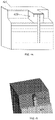
- Si or SiGe fins may be formed after removal of the oxide ( FIG. 4m ).
- phonon scattering may limit the nanowire size to about 7nm, this may limit the long term scaling of such devices.
- One solution is to construct the devices vertically, with either the N or P channel located in a bottom wire and the other channel located in a top wire.
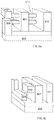
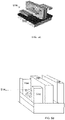
- FIG. 5a depicts an inverter done with the N+ substrate 500 for Vss and gate 501. Note that this needs a tall contact 512 (TCN) to connect N and P nanowire channels 514, a short top TCN 510 to couple with one of the N and P nanowire channels 514, and a substrate plug 508/bottom TCN coupled to one of the N and P nanowire channels 514 and to the substrate 500.
- TCN tall contact 512
- FIG. 5b depicts a misaligned top 510 and bottom 508 TCN.
- FIG. 5c depicts N and P nanowires in comprising left and right wing nanowire structures 514.
- FIG.5d shows an inverter wired with the left and right wing nanowire structures 514.
- Nanowires with GAA offer improvement over GAA non-nanowire structures, as well as fins, and trigate structures.
- the use of lateral nanowires with replacement metal-gate (RMG), gate-all-around processing is a logical extension of the roadmap from planar with RMG, to fins with RMG.
- Gate-all-around (GAA) nanowire structures offer the potential for improved short channel control over GAA non-nanowire structures and fins. Improved Isolation of the bottom wire in a silicon or silicon germanium nanowire structure from the substrate may be achieved according to examples herein.
- Density scaling when the smallest nanowire size is limited to > ⁇ 7nm due to phonon scattering may be enabled. Lateral nanowire structures for both silicon and silicon germanium may be incorporated with replacement metal-gate architecture and manufacturing-compatible fabrication techniques for the wires modified from those developed for trigate structures. Vertical architecture scaling with nanowires is enabled. Building circuits in the transistor layer itself using nanowires is enabled herein.
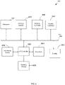
- FIG. 6 shows a computer system.
- System 600 includes a processor 610, a memory device 620, a memory controller 630, a graphics controller 640, an input and output (I/O) controller 650, a display 652, a keyboard 654, a pointing device 656, and a peripheral device 658, all of which may be communicatively coupled to each other through a bus 660.
- Processor 610 may be a general purpose processor or an application specific integrated circuit (ASIC).
- I/O controller 650 may include a communication module for wired or wireless communication.
- Memory device 620 may be a dynamic random access memory (DRAM) device, a static random access memory (SRAM) device, a flash memory device, or a combination of these memory devices. Thus, memory device 620 in system 600 does not have to include a DRAM device.
- DRAM dynamic random access memory
- SRAM static random access memory
- flash memory device or a combination of these memory devices.
- processor 610 may include one or more nanowire devices of the various examples included herein.
- memory device 620 or at least a portion of I/O controller 650, or a combination of these components may include in an integrated circuit package that includes at least one example of the structures herein.
- memory device 620 may be used in some cases to provide long-term storage for the executable instructions for a method for forming structures in accordance with some embodiments, and in other examples may be used to store on a shorter term basis the executable instructions of a method for forming structures in accordance with embodiments during execution by processor 710.
- the instructions may be stored, or otherwise associated with, machine accessible mediums communicatively coupled with the system, such as compact disk read only memories (CD-ROMs), digital versatile disks (DVDs), and floppy disks, carrier waves, and/or other propagated signals, for example.
- memory device 620 may supply the processor 610 with the executable instructions for execution.
- System 600 may include computers (e.g., desktops, laptops, hand-helds, servers, Web appliances, routers, etc.), wireless communication devices (e.g., cellular phones, cordless phones, pagers, personal digital assistants, etc.), computer-related peripherals (e.g., printers, scanners, monitors, etc.), entertainment devices (e.g., televisions, radios, stereos, tape and compact disc players, video cassette recorders, camcorders, digital cameras, MP3 (Motion Picture Experts Group, Audio Layer 3) players, video games, watches, etc.), and the like.
- computers e.g., desktops, laptops, hand-helds, servers, Web appliances, routers, etc.
- wireless communication devices e.g., cellular phones, cordless phones, pagers, personal digital assistants, etc.
- computer-related peripherals e.g., printers, scanners, monitors, etc.
- entertainment devices e.g., televisions, radios, stereos, tape and
Landscapes
- Engineering & Computer Science (AREA)
- Chemical & Material Sciences (AREA)
- Nanotechnology (AREA)
- Crystallography & Structural Chemistry (AREA)
- Theoretical Computer Science (AREA)
- Physics & Mathematics (AREA)
- Mathematical Physics (AREA)
- Insulated Gate Type Field-Effect Transistor (AREA)
- Thin Film Transistor (AREA)
- Metal-Oxide And Bipolar Metal-Oxide Semiconductor Integrated Circuits (AREA)
- Silicon Compounds (AREA)
- Electrodes Of Semiconductors (AREA)
- Materials Engineering (AREA)
Claims (3)
- Procédé de formation d'une partie d'un dispositif à nanofils à grille enrobante comprenant :la formation d'un empilement (120) de couches alternées de silicium-germanium épitaxial (102, 102') et de silicium épitaxial (104, 104') sur un substrat (100), l'empilement (120) comprenant une pluralité de couches de silicium-germanium épitaxial (102, 102') et une pluralité de couches de silicium épitaxial (104, 104') ;le modelage dudit empilement (120) pour former une pluralité de structures d'aileron (107) séparées par des tranchées (101), le modelage comprenant la gravure dudit empilement (120) ;la formation d'une pluralité d'entretoises (106) d'un bout à l'autre et sur la pluralité de structures d'aileron (107) ;la formation d'une électrode de grille sacrificielle (108) entre la pluralité d'entretoises (106) et autour de parties de la pluralité de structures d'aileron (107) situées entre les entretoises (106) ;le retrait d'une partie de chacune de la pluralité de structures d'aileron (107) du substrat (100), la partie n'étant pas située entre les entretoises (106), pour exposer une pluralité respective de régions de source/drain (109) sur le substrat (100), la pluralité de régions de source/drain (109) étant adjacentes à la pluralité d'entretoises (106) ;la formation d'une structure de source/drain épitaxiale (110) dans chacune de la pluralité de régions de source/drain (109) ;le retrait de l'électrode de grille sacrificielle (108) des emplacements entre la pluralité d'entretoises (106) ;le retrait de la pluralité de couches de silicium épitaxial ou de la pluralité de couches de silicium-germanium épitaxial de la pluralité de structures d'aileron (107) disposées entre la pluralité d'entretoises (106) pour former une pluralité de structures de nanofil de silicium-germanium (104, 104') ou une pluralité de structures de nanofil de silicium (102, 102'), respectivement ;le dépôt d'un matériau diélectrique de grille (115) autour de chacune de la pluralité de structures de nanofil de silicium-germanium (104, 104') ou autour de chacune de la pluralité de structures de nanofil de silicium (102, 102') ; etla formation d'un matériau d'électrode de grille (117) autour du matériau diélectrique de grille (115), dans lequel le matériau d'électrode de grille (117) entoure la pluralité de structures de nanofil de silicium-germanium (104, 104') ou la pluralité de structures de nanofil de silicium (102, 102'), et remplit un espace entre la pluralité de structures de nanofil de silicium-germanium (104, 104') ou entre la pluralité de structures de nanofil de silicium (102, 102').
- Procédé de la revendication 1 dans lequel le matériau diélectrique de grille (115) est formé autour de tous les côtés des structures de nanofil de silicium-germanium.
- Procédé de la revendication 1 dans lequel le matériau diélectrique de grille (115) est formé autour de tous les côtés des structures de nanofil de silicium.
Priority Applications (2)
| Application Number | Priority Date | Filing Date | Title |
|---|---|---|---|
| EP15166618.7A EP2942817B1 (fr) | 2010-12-01 | 2011-11-23 | Structures à nanofils de silicium et de silicium-germanium |
| EP23167162.9A EP4235801A3 (fr) | 2010-12-01 | 2011-11-23 | Structures à nanofils de silicium et de silicium-germanium |
Applications Claiming Priority (2)
| Application Number | Priority Date | Filing Date | Title |
|---|---|---|---|
| US12/958,179 US8753942B2 (en) | 2010-12-01 | 2010-12-01 | Silicon and silicon germanium nanowire structures |
| PCT/US2011/062059 WO2012074872A2 (fr) | 2010-12-01 | 2011-11-23 | Structures à nanofils de silicium et de silicium-germanium |
Related Child Applications (3)
| Application Number | Title | Priority Date | Filing Date |
|---|---|---|---|
| EP23167162.9A Division EP4235801A3 (fr) | 2010-12-01 | 2011-11-23 | Structures à nanofils de silicium et de silicium-germanium |
| EP15166618.7A Division EP2942817B1 (fr) | 2010-12-01 | 2011-11-23 | Structures à nanofils de silicium et de silicium-germanium |
| EP15166618.7A Division-Into EP2942817B1 (fr) | 2010-12-01 | 2011-11-23 | Structures à nanofils de silicium et de silicium-germanium |
Publications (3)
| Publication Number | Publication Date |
|---|---|
| EP2647038A2 EP2647038A2 (fr) | 2013-10-09 |
| EP2647038A4 EP2647038A4 (fr) | 2015-01-07 |
| EP2647038B1 true EP2647038B1 (fr) | 2022-10-12 |
Family
ID=46161357
Family Applications (3)
| Application Number | Title | Priority Date | Filing Date |
|---|---|---|---|
| EP15166618.7A Active EP2942817B1 (fr) | 2010-12-01 | 2011-11-23 | Structures à nanofils de silicium et de silicium-germanium |
| EP11844167.4A Active EP2647038B1 (fr) | 2010-12-01 | 2011-11-23 | Structures à nanofils en silicium et en silicium-germanium |
| EP23167162.9A Pending EP4235801A3 (fr) | 2010-12-01 | 2011-11-23 | Structures à nanofils de silicium et de silicium-germanium |
Family Applications Before (1)
| Application Number | Title | Priority Date | Filing Date |
|---|---|---|---|
| EP15166618.7A Active EP2942817B1 (fr) | 2010-12-01 | 2011-11-23 | Structures à nanofils de silicium et de silicium-germanium |
Family Applications After (1)
| Application Number | Title | Priority Date | Filing Date |
|---|---|---|---|
| EP23167162.9A Pending EP4235801A3 (fr) | 2010-12-01 | 2011-11-23 | Structures à nanofils de silicium et de silicium-germanium |
Country Status (7)
| Country | Link |
|---|---|
| US (7) | US8753942B2 (fr) |
| EP (3) | EP2942817B1 (fr) |
| JP (5) | JP2014505995A (fr) |
| KR (10) | KR101536837B1 (fr) |
| CN (5) | CN114242763A (fr) |
| SG (3) | SG190373A1 (fr) |
| WO (1) | WO2012074872A2 (fr) |
Families Citing this family (275)
| Publication number | Priority date | Publication date | Assignee | Title |
|---|---|---|---|---|
| US8558279B2 (en) * | 2010-09-23 | 2013-10-15 | Intel Corporation | Non-planar device having uniaxially strained semiconductor body and method of making same |
| US8753942B2 (en) | 2010-12-01 | 2014-06-17 | Intel Corporation | Silicon and silicon germanium nanowire structures |
| US8987794B2 (en) * | 2011-12-23 | 2015-03-24 | Intel Coporation | Non-planar gate all-around device and method of fabrication thereof |
| US9224808B2 (en) | 2011-12-23 | 2015-12-29 | Intel Corporation | Uniaxially strained nanowire structure |
| WO2013095656A1 (fr) * | 2011-12-23 | 2013-06-27 | Intel Corporation | Dispositifs semi-conducteurs à substrat commun ayant des nanofils ou des corps semi-conducteurs à orientation ou composition de matériau différentes |
| US9012284B2 (en) | 2011-12-23 | 2015-04-21 | Intel Corporation | Nanowire transistor devices and forming techniques |
| WO2013095646A1 (fr) | 2011-12-23 | 2013-06-27 | Intel Corporation | Structure à nanofils cmos |
| WO2013095650A1 (fr) | 2011-12-23 | 2013-06-27 | Intel Corporation | Structures à nanofils ayant des zones de source et de drain non discrètes |
| WO2013101237A1 (fr) * | 2011-12-31 | 2013-07-04 | Intel Corporation | Arrêt de gravure de masque dur destiné à de grandes ailettes |
| FR2989515B1 (fr) * | 2012-04-16 | 2015-01-16 | Commissariat Energie Atomique | Procede ameliore de realisation d'une structure de transistor a nano-fils superposes et a grille enrobante |
| US9484447B2 (en) | 2012-06-29 | 2016-11-01 | Intel Corporation | Integration methods to fabricate internal spacers for nanowire devices |
| US9142400B1 (en) | 2012-07-17 | 2015-09-22 | Stc.Unm | Method of making a heteroepitaxial layer on a seed area |
| KR101678405B1 (ko) * | 2012-07-27 | 2016-11-22 | 인텔 코포레이션 | 나노와이어 트랜지스터 디바이스 및 형성 기법 |
| US8703556B2 (en) * | 2012-08-30 | 2014-04-22 | Taiwan Semiconductor Manufacturing Company, Ltd. | Method of making a FinFET device |
| US8889564B2 (en) | 2012-08-31 | 2014-11-18 | International Business Machines Corporation | Suspended nanowire structure |
| US8735869B2 (en) | 2012-09-27 | 2014-05-27 | Intel Corporation | Strained gate-all-around semiconductor devices formed on globally or locally isolated substrates |
| US8823059B2 (en) | 2012-09-27 | 2014-09-02 | Intel Corporation | Non-planar semiconductor device having group III-V material active region with multi-dielectric gate stack |
| US8785909B2 (en) | 2012-09-27 | 2014-07-22 | Intel Corporation | Non-planar semiconductor device having channel region with low band-gap cladding layer |
| US9041106B2 (en) * | 2012-09-27 | 2015-05-26 | Intel Corporation | Three-dimensional germanium-based semiconductor devices formed on globally or locally isolated substrates |
| US20140091279A1 (en) | 2012-09-28 | 2014-04-03 | Jessica S. Kachian | Non-planar semiconductor device having germanium-based active region with release etch-passivation surface |
| US8765563B2 (en) * | 2012-09-28 | 2014-07-01 | Intel Corporation | Trench confined epitaxially grown device layer(s) |
| KR102002380B1 (ko) * | 2012-10-10 | 2019-07-23 | 삼성전자 주식회사 | 반도체 장치 및 그 제조 방법 |
| KR101994079B1 (ko) * | 2012-10-10 | 2019-09-30 | 삼성전자 주식회사 | 반도체 장치 및 그 제조 방법 |
| US8653599B1 (en) | 2012-11-16 | 2014-02-18 | International Business Machines Corporation | Strained SiGe nanowire having (111)-oriented sidewalls |
| US8759874B1 (en) * | 2012-11-30 | 2014-06-24 | Stmicroelectronics, Inc. | FinFET device with isolated channel |
| US20140167163A1 (en) * | 2012-12-17 | 2014-06-19 | International Business Machines Corporation | Multi-Fin FinFETs with Epitaxially-Grown Merged Source/Drains |
| US8956942B2 (en) | 2012-12-21 | 2015-02-17 | Stmicroelectronics, Inc. | Method of forming a fully substrate-isolated FinFET transistor |
| US8969145B2 (en) | 2013-01-19 | 2015-03-03 | International Business Machines Corporation | Wire-last integration method and structure for III-V nanowire devices |
| KR102049774B1 (ko) | 2013-01-24 | 2019-11-28 | 삼성전자 주식회사 | 반도체 장치 및 그 제조 방법 |
| JP6251604B2 (ja) * | 2013-03-11 | 2017-12-20 | ルネサスエレクトロニクス株式会社 | フィンfet構造を有する半導体装置及びその製造方法 |
| US8900959B2 (en) | 2013-03-12 | 2014-12-02 | International Business Machines Corporation | Non-replacement gate nanomesh field effect transistor with pad regions |
| US8778768B1 (en) | 2013-03-12 | 2014-07-15 | International Business Machines Corporation | Non-replacement gate nanomesh field effect transistor with epitixially grown source and drain |
| US8951870B2 (en) * | 2013-03-14 | 2015-02-10 | International Business Machines Corporation | Forming strained and relaxed silicon and silicon germanium fins on the same wafer |
| US8906768B2 (en) * | 2013-03-15 | 2014-12-09 | GlobalFoundries, Inc. | Wrap around stressor formation |
| DE112013006525B4 (de) * | 2013-03-15 | 2024-08-29 | Sony Corporation | Herstellung eines Nanodrahttransistors Hartmaskenschichten |
| US8940602B2 (en) * | 2013-04-11 | 2015-01-27 | International Business Machines Corporation | Self-aligned structure for bulk FinFET |
| CN104124157B (zh) * | 2013-04-23 | 2016-12-28 | 中芯国际集成电路制造(上海)有限公司 | 半导体装置及其制造方法 |
| US8987082B2 (en) | 2013-05-31 | 2015-03-24 | Stmicroelectronics, Inc. | Method of making a semiconductor device using sacrificial fins |
| US9082788B2 (en) | 2013-05-31 | 2015-07-14 | Stmicroelectronics, Inc. | Method of making a semiconductor device including an all around gate |
| US20140353716A1 (en) | 2013-05-31 | 2014-12-04 | Stmicroelectronics, Inc | Method of making a semiconductor device using a dummy gate |
| US8962408B2 (en) | 2013-06-04 | 2015-02-24 | International Business Machines Corporation | Replacement gate self-aligned carbon nanostructure transistor |
| KR102220806B1 (ko) | 2013-06-20 | 2021-02-26 | 인텔 코포레이션 | 도핑된 서브-핀 영역을 갖는 비평면 반도체 디바이스 및 그 제조 방법 |
| US9035277B2 (en) | 2013-08-01 | 2015-05-19 | Taiwan Semiconductor Manufacturing Company, Ltd. | Semiconductor device and fabricating the same |
| US9171843B2 (en) * | 2013-08-02 | 2015-10-27 | Taiwan Semiconductor Manufacturing Company, Ltd. | Semiconductor device and fabricating the same |
| KR102069609B1 (ko) * | 2013-08-12 | 2020-01-23 | 삼성전자주식회사 | 반도체 소자 및 그 제조 방법 |
| US9184269B2 (en) * | 2013-08-20 | 2015-11-10 | Taiwan Semiconductor Manufacturing Company Limited | Silicon and silicon germanium nanowire formation |
| US11404325B2 (en) | 2013-08-20 | 2022-08-02 | Taiwan Semiconductor Manufacturing Co., Ltd. | Silicon and silicon germanium nanowire formation |
| US9059002B2 (en) * | 2013-08-27 | 2015-06-16 | International Business Machines Corporation | Non-merged epitaxially grown MOSFET devices |
| US9252016B2 (en) * | 2013-09-04 | 2016-02-02 | Globalfoundries Inc. | Stacked nanowire |
| US9508796B2 (en) * | 2013-10-03 | 2016-11-29 | Intel Corporation | Internal spacers for nanowire transistors and method of fabrication thereof |
| KR102085525B1 (ko) | 2013-11-27 | 2020-03-09 | 삼성전자 주식회사 | 반도체 장치 및 그 제조 방법 |
| US20150170916A1 (en) * | 2013-12-17 | 2015-06-18 | United Microelectronics Corp. | Semiconductor process for manufacturing epitaxial structures |
| WO2015094301A1 (fr) | 2013-12-19 | 2015-06-25 | Intel Corporation | Dispositif semi-conducteur non plan possédant une région active à base de géométrie hybride |
| KR102135303B1 (ko) * | 2013-12-27 | 2020-07-17 | 인텔 코포레이션 | 확산된 팁 연장 트랜지스터 |
| CN103700578B (zh) * | 2013-12-27 | 2017-03-01 | 中国科学院微电子研究所 | 一种锗硅纳米线叠层结构的制作方法 |
| US9159552B2 (en) | 2013-12-27 | 2015-10-13 | Taiwan Semiconductor Manufacturing Company, Ltd. | Method of forming a germanium-containing FinFET |
| US9087900B1 (en) | 2014-01-07 | 2015-07-21 | Samsung Electronics Co., Ltd. | Semiconductor device and method for fabricating the same |
| US9853154B2 (en) * | 2014-01-24 | 2017-12-26 | Taiwan Semiconductor Manufacturing Company Ltd. | Embedded source or drain region of transistor with downward tapered region under facet region |
| KR102155181B1 (ko) | 2014-01-28 | 2020-09-11 | 삼성전자주식회사 | 반도체 장치 및 그 제조 방법 |
| US9263584B2 (en) | 2014-02-11 | 2016-02-16 | International Business Machines Corporation | Field effect transistors employing a thin channel region on a crystalline insulator structure |
| US9257527B2 (en) | 2014-02-14 | 2016-02-09 | International Business Machines Corporation | Nanowire transistor structures with merged source/drain regions using auxiliary pillars |
| US9224811B2 (en) | 2014-03-17 | 2015-12-29 | Globalfoundries Inc | Stacked semiconductor device |
| US9780216B2 (en) * | 2014-03-19 | 2017-10-03 | Taiwan Semiconductor Manufacturing Company, Ltd. | Combination FinFET and methods of forming same |
| EP3123520A4 (fr) | 2014-03-28 | 2017-11-22 | Intel Corporation | Contact supérieur mis à nouveau à croître de façon sélective pour des dispositifs verticaux à semi-conducteurs |
| CN104979211B (zh) | 2014-04-10 | 2018-03-06 | 中芯国际集成电路制造(上海)有限公司 | 纳米线器件及其制造方法 |
| US9093478B1 (en) | 2014-04-11 | 2015-07-28 | International Business Machines Corporation | Integrated circuit structure with bulk silicon FinFET and methods of forming |
| US9601576B2 (en) * | 2014-04-18 | 2017-03-21 | International Business Machines Corporation | Nanowire FET with tensile channel stressor |
| US9230992B2 (en) | 2014-04-30 | 2016-01-05 | International Business Machines Corporation | Semiconductor device including gate channel having adjusted threshold voltage |
| KR102146469B1 (ko) | 2014-04-30 | 2020-08-21 | 삼성전자 주식회사 | 반도체 장치 및 이의 제조 방법 |
| KR102158961B1 (ko) | 2014-05-13 | 2020-09-24 | 삼성전자 주식회사 | 반도체 장치 및 그 제조 방법 |
| US9548358B2 (en) | 2014-05-19 | 2017-01-17 | International Business Machines Corporation | Dual fill silicon-on-nothing field effect transistor |
| US9287357B2 (en) * | 2014-06-16 | 2016-03-15 | Samsung Electronics Co., Ltd. | Integrated circuits with Si and non-Si nanosheet FET co-integration with low band-to-band tunneling and methods of fabricating the same |
| US9577100B2 (en) * | 2014-06-16 | 2017-02-21 | Globalfoundries Inc. | FinFET and nanowire semiconductor devices with suspended channel regions and gate structures surrounding the suspended channel regions |
| US9431512B2 (en) * | 2014-06-18 | 2016-08-30 | Globalfoundries Inc. | Methods of forming nanowire devices with spacers and the resulting devices |
| US9490340B2 (en) | 2014-06-18 | 2016-11-08 | Globalfoundries Inc. | Methods of forming nanowire devices with doped extension regions and the resulting devices |
| US9543440B2 (en) * | 2014-06-20 | 2017-01-10 | International Business Machines Corporation | High density vertical nanowire stack for field effect transistor |
| US9502518B2 (en) * | 2014-06-23 | 2016-11-22 | Stmicroelectronics, Inc. | Multi-channel gate-all-around FET |
| US9224736B1 (en) | 2014-06-27 | 2015-12-29 | Taiwan Semicondcutor Manufacturing Company, Ltd. | Structure and method for SRAM FinFET device |
| US9966471B2 (en) | 2014-06-27 | 2018-05-08 | Taiwan Semiconductor Manufacturing Company, Ltd. | Stacked Gate-All-Around FinFET and method forming the same |
| US9881993B2 (en) * | 2014-06-27 | 2018-01-30 | Taiwan Semiconductor Manufacturing Company Limited | Method of forming semiconductor structure with horizontal gate all around structure |
| US9608116B2 (en) * | 2014-06-27 | 2017-03-28 | Taiwan Semiconductor Manufacturing Company, Ltd. | FINFETs with wrap-around silicide and method forming the same |
| US9443978B2 (en) | 2014-07-14 | 2016-09-13 | Samsung Electronics Co., Ltd. | Semiconductor device having gate-all-around transistor and method of manufacturing the same |
| US9306019B2 (en) * | 2014-08-12 | 2016-04-05 | GlobalFoundries, Inc. | Integrated circuits with nanowires and methods of manufacturing the same |
| KR101628197B1 (ko) * | 2014-08-22 | 2016-06-09 | 삼성전자주식회사 | 반도체 소자의 제조 방법 |
| US9293588B1 (en) | 2014-08-28 | 2016-03-22 | International Business Machines Corporation | FinFET with a silicon germanium alloy channel and method of fabrication thereof |
| US9343529B2 (en) * | 2014-09-05 | 2016-05-17 | International Business Machines Corporation | Method of formation of germanium nanowires on bulk substrates |
| US9793356B2 (en) | 2014-09-12 | 2017-10-17 | Samsung Electronics Co., Ltd. | Semiconductor device and method for fabricating the same |
| US9318553B1 (en) | 2014-10-16 | 2016-04-19 | International Business Machines Corporation | Nanowire device with improved epitaxy |
| US20160141360A1 (en) * | 2014-11-19 | 2016-05-19 | International Business Machines Corporation | Iii-v semiconductor devices with selective oxidation |
| US9391201B2 (en) | 2014-11-25 | 2016-07-12 | Taiwan Semiconductor Manufacturing Company, Ltd. | Source/drain structure and manufacturing the same |
| US9660059B2 (en) | 2014-12-12 | 2017-05-23 | International Business Machines Corporation | Fin replacement in a field-effect transistor |
| US9449820B2 (en) | 2014-12-22 | 2016-09-20 | International Business Machines Corporation | Epitaxial growth techniques for reducing nanowire dimension and pitch |
| TWI598994B (zh) | 2015-01-13 | 2017-09-11 | 東京威力科創股份有限公司 | 奈米線結構之形成方法 |
| TWI629790B (zh) * | 2015-01-26 | 2018-07-11 | 聯華電子股份有限公司 | 半導體元件及其製作方法 |
| US9508795B2 (en) * | 2015-02-04 | 2016-11-29 | Globalfoundries Inc. | Methods of fabricating nanowire structures |
| CN106033725B (zh) | 2015-03-13 | 2020-10-16 | 联华电子股份有限公司 | 半导体元件及其制作工艺 |
| US9349860B1 (en) | 2015-03-31 | 2016-05-24 | Taiwan Semiconductor Manufacturing Company, Ltd. | Field effect transistors and methods of forming same |
| US9306001B1 (en) | 2015-04-14 | 2016-04-05 | International Business Machines Corporation | Uniformly doped leakage current stopper to counter under channel leakage currents in bulk FinFET devices |
| US9793403B2 (en) | 2015-04-14 | 2017-10-17 | Samsung Electronics Co., Ltd. | Multi-layer fin field effect transistor devices and methods of forming the same |
| US9748364B2 (en) * | 2015-04-21 | 2017-08-29 | Varian Semiconductor Equipment Associates, Inc. | Method for fabricating three dimensional device |
| US9893161B2 (en) | 2015-04-22 | 2018-02-13 | Tokyo Electron Limited | Parasitic capacitance reduction structure for nanowire transistors and method of manufacturing |
| KR102380818B1 (ko) * | 2015-04-30 | 2022-03-31 | 삼성전자주식회사 | 반도체 소자 |
| US9437502B1 (en) | 2015-06-12 | 2016-09-06 | International Business Machines Corporation | Method to form stacked germanium nanowires and stacked III-V nanowires |
| US10134840B2 (en) | 2015-06-15 | 2018-11-20 | International Business Machines Corporation | Series resistance reduction in vertically stacked silicon nanowire transistors |
| US10170608B2 (en) | 2015-06-30 | 2019-01-01 | International Business Machines Corporation | Internal spacer formation from selective oxidation for fin-first wire-last replacement gate-all-around nanowire FET |
| EP3112316B1 (fr) * | 2015-07-02 | 2018-05-02 | IMEC vzw | Procédé de fabrication de transistors comprenant multiples canaux nanofils |
| US9425259B1 (en) * | 2015-07-17 | 2016-08-23 | Samsung Electronics Co., Ltd. | Semiconductor device having a fin |
| US9614068B2 (en) | 2015-09-02 | 2017-04-04 | Samsung Electronics Co., Ltd. | Semiconductor device and method of fabricating the same |
| US9647139B2 (en) | 2015-09-04 | 2017-05-09 | International Business Machines Corporation | Atomic layer deposition sealing integration for nanosheet complementary metal oxide semiconductor with replacement spacer |
| CN113611610B (zh) * | 2015-09-10 | 2025-04-04 | 英特尔公司 | 具有腔间隔器的半导体纳米线装置和制造半导体纳米线装置的腔间隔器的方法 |
| WO2017044117A1 (fr) * | 2015-09-11 | 2017-03-16 | Intel Corporation | Transistors à canaux de germanium et sous-ailette de phosphure d'aluminium-indium |
| US9437501B1 (en) | 2015-09-22 | 2016-09-06 | International Business Machines Corporation | Stacked nanowire device width adjustment by gas cluster ion beam (GCIB) |
| US9608099B1 (en) | 2015-09-22 | 2017-03-28 | International Business Machines Corporation | Nanowire semiconductor device |
| US10879241B2 (en) | 2015-09-25 | 2020-12-29 | Intel Corporation | Techniques for controlling transistor sub-fin leakage |
| US9716142B2 (en) | 2015-10-12 | 2017-07-25 | International Business Machines Corporation | Stacked nanowires |
| KR102379701B1 (ko) | 2015-10-19 | 2022-03-28 | 삼성전자주식회사 | 멀티-채널을 갖는 반도체 소자 및 그 형성 방법 |
| US9741792B2 (en) | 2015-10-21 | 2017-08-22 | International Business Machines Corporation | Bulk nanosheet with dielectric isolation |
| US9496263B1 (en) * | 2015-10-23 | 2016-11-15 | International Business Machines Corporation | Stacked strained and strain-relaxed hexagonal nanowires |
| US9590038B1 (en) * | 2015-10-23 | 2017-03-07 | Samsung Electronics Co., Ltd. | Semiconductor device having nanowire channel |
| US10177143B2 (en) * | 2015-10-28 | 2019-01-08 | Taiwan Semiconductor Manufacturing Company Limited | FinFET device and method for fabricating the same |
| KR102557215B1 (ko) | 2015-10-30 | 2023-07-18 | 유니버시티 오브 플로리다 리서치 파운데이션, 인크. | 캡슐화된 나노구조체 및 제조 방법 |
| US9362355B1 (en) | 2015-11-13 | 2016-06-07 | International Business Machines Corporation | Nanosheet MOSFET with full-height air-gap spacer |
| US9754840B2 (en) | 2015-11-16 | 2017-09-05 | Taiwan Semiconductor Manufacturing Company, Ltd. | Horizontal gate-all-around device having wrapped-around source and drain |
| US9899387B2 (en) * | 2015-11-16 | 2018-02-20 | Taiwan Semiconductor Manufacturing Company, Ltd. | Multi-gate device and method of fabrication thereof |
| US9559013B1 (en) * | 2015-11-23 | 2017-01-31 | International Business Machines Corporation | Stacked nanowire semiconductor device |
| US10164121B2 (en) * | 2015-11-25 | 2018-12-25 | Samsung Electronics Co., Ltd. | Stacked independently contacted field effect transistor having electrically separated first and second gates |
| US10164012B2 (en) * | 2015-11-30 | 2018-12-25 | Taiwan Semiconductor Manufacturing Co., Ltd. | Semiconductor device and manufacturing method thereof |
| US9425291B1 (en) | 2015-12-09 | 2016-08-23 | International Business Machines Corporation | Stacked nanosheets by aspect ratio trapping |
| KR102434993B1 (ko) * | 2015-12-09 | 2022-08-24 | 삼성전자주식회사 | 반도체 소자 |
| US9431301B1 (en) | 2015-12-10 | 2016-08-30 | International Business Machines Corporation | Nanowire field effect transistor (FET) and method for fabricating the same |
| US10497701B2 (en) | 2015-12-16 | 2019-12-03 | Taiwan Semiconductor Manufacturing Co., Ltd. | Semiconductor device and manufacturing method thereof |
| EP3394896B1 (fr) * | 2015-12-24 | 2025-10-08 | Tahoe Research, Ltd. | Procédés de formation de contacts source/drain dopés et structures formées de cette façon |
| US10157992B2 (en) | 2015-12-28 | 2018-12-18 | Qualcomm Incorporated | Nanowire device with reduced parasitics |
| US9722022B2 (en) | 2015-12-28 | 2017-08-01 | International Business Machines Corporation | Sidewall image transfer nanosheet |
| US9899269B2 (en) * | 2015-12-30 | 2018-02-20 | Taiwan Semiconductor Manufacturing Company, Ltd | Multi-gate device and method of fabrication thereof |
| KR102367408B1 (ko) * | 2016-01-04 | 2022-02-25 | 삼성전자주식회사 | 복수의 시트들로 구성된 채널 영역을 포함하는 sram 소자 |
| KR102366953B1 (ko) * | 2016-01-06 | 2022-02-23 | 삼성전자주식회사 | 반도체 장치 및 이의 제조 방법 |
| US10074730B2 (en) * | 2016-01-28 | 2018-09-11 | International Business Machines Corporation | Forming stacked nanowire semiconductor device |
| US9614040B1 (en) | 2016-02-02 | 2017-04-04 | International Business Machines Corporation | Strained silicon germanium fin with block source/drain epitaxy and improved overlay capacitance |
| KR102461174B1 (ko) | 2016-02-26 | 2022-11-01 | 삼성전자주식회사 | 반도체 소자 |
| US9748404B1 (en) * | 2016-02-29 | 2017-08-29 | International Business Machines Corporation | Method for fabricating a semiconductor device including gate-to-bulk substrate isolation |
| CN107204311A (zh) * | 2016-03-16 | 2017-09-26 | 上海新昇半导体科技有限公司 | 纳米线半导体器件及其制造方法 |
| US9978649B2 (en) | 2016-03-21 | 2018-05-22 | Tokyo Electron Limited | Solid source doping for source and drain extension doping |
| US9735269B1 (en) * | 2016-05-06 | 2017-08-15 | International Business Machines Corporation | Integrated strained stacked nanosheet FET |
| FR3051970B1 (fr) | 2016-05-25 | 2020-06-12 | Commissariat A L'energie Atomique Et Aux Energies Alternatives | Realisation d'une structure de canal formee d'une pluralite de barreaux semi-conducteurs contraints |
| US11004985B2 (en) | 2016-05-30 | 2021-05-11 | Samsung Electronics Co., Ltd. | Semiconductor device having multi-thickness nanowire |
| KR20170135115A (ko) | 2016-05-30 | 2017-12-08 | 삼성전자주식회사 | 반도체 장치 및 그 제조 방법 |
| KR102429611B1 (ko) | 2016-06-10 | 2022-08-04 | 삼성전자주식회사 | 반도체 장치 제조 방법 |
| CN105977299B (zh) * | 2016-06-17 | 2019-12-10 | 中国科学院微电子研究所 | 半导体器件及其制造方法 |
| KR102527382B1 (ko) * | 2016-06-21 | 2023-04-28 | 삼성전자주식회사 | 반도체 소자 |
| US10134905B2 (en) * | 2016-06-30 | 2018-11-20 | International Business Machines Corporation | Semiconductor device including wrap around contact, and method of forming the semiconductor device |
| US10236362B2 (en) * | 2016-06-30 | 2019-03-19 | International Business Machines Corporation | Nanowire FET including nanowire channel spacers |
| US10453850B2 (en) | 2016-07-19 | 2019-10-22 | Tokyo Electron Limited | Three-dimensional semiconductor device including integrated circuit, transistors and transistor components and method of fabrication |
| TWI731138B (zh) * | 2016-08-08 | 2021-06-21 | 日商東京威力科創股份有限公司 | 三維半導體裝置及其製造方法 |
| TWI739879B (zh) * | 2016-08-10 | 2021-09-21 | 日商東京威力科創股份有限公司 | 用於半導體裝置的延伸區域 |
| US10840381B2 (en) | 2016-08-10 | 2020-11-17 | International Business Machines Corporation | Nanosheet and nanowire MOSFET with sharp source/drain junction |
| US10026652B2 (en) * | 2016-08-17 | 2018-07-17 | Samsung Electronics Co., Ltd. | Horizontal nanosheet FETs and method of manufacturing the same |
| US10332986B2 (en) | 2016-08-22 | 2019-06-25 | International Business Machines Corporation | Formation of inner spacer on nanosheet MOSFET |
| US9905643B1 (en) | 2016-08-26 | 2018-02-27 | International Business Machines Corporation | Vertically aligned nanowire channels with source/drain interconnects for nanosheet transistors |
| US9704863B1 (en) | 2016-09-09 | 2017-07-11 | International Business Machines Corporation | Forming a hybrid channel nanosheet semiconductor structure |
| US9620590B1 (en) * | 2016-09-20 | 2017-04-11 | International Business Machines Corporation | Nanosheet channel-to-source and drain isolation |
| US9704995B1 (en) * | 2016-09-20 | 2017-07-11 | Advanced Micro Devices, Inc. | Gate all around device architecture with local oxide |
| US9728621B1 (en) * | 2016-09-28 | 2017-08-08 | International Business Machines Corporation | iFinFET |
| KR102326463B1 (ko) | 2016-11-14 | 2021-11-12 | 도쿄엘렉트론가부시키가이샤 | 나노와이어 및 나노슬랩 처리를 위해 벌크 실리콘으로 전하가 이동하는 것을 방지하는 방법 |
| CN111370466A (zh) | 2016-11-21 | 2020-07-03 | 华为技术有限公司 | 一种场效应晶体管及其制作方法 |
| CN108231589B (zh) * | 2016-12-09 | 2020-06-05 | Imec 非营利协会 | 纳米线半导体器件中内间隔的形成 |
| WO2018118007A1 (fr) * | 2016-12-19 | 2018-06-28 | Intel Corporation | Condensation permettant un contrôle de contrainte |
| US9972542B1 (en) | 2017-01-04 | 2018-05-15 | International Business Machines Corporation | Hybrid-channel nano-sheet FETs |
| KR102564325B1 (ko) | 2017-01-04 | 2023-08-07 | 삼성전자주식회사 | 다수의 채널 영역을 가지는 반도체 장치 |
| US9935014B1 (en) | 2017-01-12 | 2018-04-03 | International Business Machines Corporation | Nanosheet transistors having different gate dielectric thicknesses on the same chip |
| US10068794B2 (en) * | 2017-01-31 | 2018-09-04 | Advanced Micro Devices, Inc. | Gate all around device architecture with hybrid wafer bond technique |
| US9881998B1 (en) | 2017-02-02 | 2018-01-30 | International Business Machines Corporation | Stacked nanosheet field effect transistor device with substrate isolation |
| US10050107B1 (en) | 2017-02-13 | 2018-08-14 | International Business Machines Corporation | Nanosheet transistors on bulk material |
| US10032867B1 (en) | 2017-03-07 | 2018-07-24 | International Business Machines Corporation | Forming bottom isolation layer for nanosheet technology |
| JP2018147396A (ja) * | 2017-03-08 | 2018-09-20 | 株式会社ジャパンディスプレイ | 表示装置 |
| US10381468B2 (en) * | 2017-03-21 | 2019-08-13 | International Business Machines Corporation | Method and structure for forming improved single electron transistor with gap tunnel barriers |
| US10290738B2 (en) * | 2017-04-10 | 2019-05-14 | Globalfoundries Inc. | Methods of forming epi semiconductor material on a recessed fin in the source/drain regions of a FinFET device |
| US10930793B2 (en) | 2017-04-21 | 2021-02-23 | International Business Machines Corporation | Bottom channel isolation in nanosheet transistors |
| US10186510B2 (en) | 2017-05-01 | 2019-01-22 | Advanced Micro Devices, Inc. | Vertical gate all around library architecture |
| US10304728B2 (en) | 2017-05-01 | 2019-05-28 | Advanced Micro Devices, Inc. | Double spacer immersion lithography triple patterning flow and method |
| US10121868B1 (en) | 2017-05-03 | 2018-11-06 | Globalfoundries Inc. | Methods of forming epi semiconductor material on a thinned fin in the source/drain regions of a FinFET device |
| US9954058B1 (en) | 2017-06-12 | 2018-04-24 | International Business Machines Corporation | Self-aligned air gap spacer for nanosheet CMOS devices |
| KR102414182B1 (ko) * | 2017-06-29 | 2022-06-28 | 삼성전자주식회사 | 반도체 소자 |
| US10276728B2 (en) | 2017-07-07 | 2019-04-30 | Taiwan Semiconductor Manufacturing Co., Ltd. | Semiconductor device including non-volatile memory cells |
| CN109390400A (zh) * | 2017-08-08 | 2019-02-26 | 中芯国际集成电路制造(上海)有限公司 | 环栅场效应晶体管及其形成方法 |
| US10934485B2 (en) | 2017-08-25 | 2021-03-02 | Versum Materials Us, Llc | Etching solution for selectively removing silicon over silicon-germanium alloy from a silicon-germanium/ silicon stack during manufacture of a semiconductor device |
| US10332985B2 (en) * | 2017-08-31 | 2019-06-25 | Taiwan Semiconductor Manufacturing Co., Ltd. | Semiconductor device and manufacturing method thereof |
| US10629679B2 (en) * | 2017-08-31 | 2020-04-21 | Taiwan Semiconductor Manufacturing Co., Ltd. | Method of manufacturing a semiconductor device and a semiconductor device |
| KR102353251B1 (ko) | 2017-09-28 | 2022-01-19 | 삼성전자주식회사 | 반도체 장치 및 그 제조 방법 |
| US20190103282A1 (en) | 2017-09-29 | 2019-04-04 | Versum Materials Us, Llc | Etching Solution for Simultaneously Removing Silicon and Silicon-Germanium Alloy From a Silicon-Germanium/Silicon Stack During Manufacture of a Semiconductor Device |
| US10867866B2 (en) | 2017-10-30 | 2020-12-15 | Taiwan Semiconductor Manufacturing Co., Ltd. | Semiconductor device and manufacturing method thereof |
| US10680084B2 (en) | 2017-11-10 | 2020-06-09 | Taiwan Semiconductor Manufacturing Co., Ltd. | Epitaxial structures for fin-like field effect transistors |
| US10355102B2 (en) | 2017-11-15 | 2019-07-16 | Taiwan Semiconductor Manufacturing Co., Ltd. | Semiconductor device and method of manufacturing the same |
| KR101999902B1 (ko) * | 2017-11-15 | 2019-10-01 | 도실리콘 씨오., 엘티디. | 페이싱바를 가지는 낸드 플래쉬 메모리 장치 및 그의 제조 방법 |
| US10269576B1 (en) | 2017-11-15 | 2019-04-23 | Taiwan Semiconductor Manufacturing Co., Ltd. | Etching and structures formed thereby |
| US10141403B1 (en) | 2017-11-16 | 2018-11-27 | International Business Machines Corporation | Integrating thin and thick gate dielectric nanosheet transistors on same chip |
| KR102399071B1 (ko) | 2017-11-17 | 2022-05-17 | 삼성전자주식회사 | 반도체 장치 |
| US10586853B2 (en) | 2017-11-27 | 2020-03-10 | International Business Machines Corporation | Non-planar field effect transistor devices with wrap-around source/drain contacts |
| US10312350B1 (en) | 2017-11-28 | 2019-06-04 | International Business Machines Corporation | Nanosheet with changing SiGe percentage for SiGe lateral recess |
| KR20240132108A (ko) | 2017-12-12 | 2024-09-02 | 소니 세미컨덕터 솔루션즈 가부시키가이샤 | 반도체 장치 및 그 제조 방법 |
| US10276687B1 (en) * | 2017-12-20 | 2019-04-30 | International Business Machines Corporation | Formation of self-aligned bottom spacer for vertical transistors |
| US10622208B2 (en) | 2017-12-22 | 2020-04-14 | International Business Machines Corporation | Lateral semiconductor nanotube with hexagonal shape |
| US10424651B2 (en) | 2018-01-26 | 2019-09-24 | International Business Machines Corporation | Forming nanosheet transistor using sacrificial spacer and inner spacers |
| WO2019150856A1 (fr) | 2018-01-30 | 2019-08-08 | ソニーセミコンダクタソリューションズ株式会社 | Dispositif à semi-conducteur |
| US10573521B2 (en) | 2018-01-30 | 2020-02-25 | International Business Machines Corporation | Gate metal patterning to avoid gate stack attack due to excessive wet etching |
| US10679890B2 (en) | 2018-02-01 | 2020-06-09 | International Business Machines Corporation | Nanosheet structure with isolated gate |
| TWI788501B (zh) | 2018-02-02 | 2023-01-01 | 日商索尼半導體解決方案公司 | 半導體裝置 |
| CN110233176B (zh) * | 2018-03-05 | 2022-07-22 | 中芯国际集成电路制造(北京)有限公司 | 半导体结构及其形成方法 |
| WO2019183099A1 (fr) * | 2018-03-19 | 2019-09-26 | Tokyo Electron Limited | Dispositif tridimensionnel et son procédé de formation |
| US10263100B1 (en) | 2018-03-19 | 2019-04-16 | International Business Machines Corporation | Buffer regions for blocking unwanted diffusion in nanosheet transistors |
| US10446664B1 (en) | 2018-03-20 | 2019-10-15 | International Business Machines Corporation | Inner spacer formation and contact resistance reduction in nanosheet transistors |
| US10566438B2 (en) | 2018-04-02 | 2020-02-18 | International Business Machines Corporation | Nanosheet transistor with dual inner airgap spacers |
| US10243054B1 (en) | 2018-04-03 | 2019-03-26 | International Business Machines Corporation | Integrating standard-gate and extended-gate nanosheet transistors on the same substrate |
| US10566445B2 (en) | 2018-04-03 | 2020-02-18 | International Business Machines Corporation | Gate spacer and inner spacer formation for nanosheet transistors having relatively small space between gates |
| US10971585B2 (en) | 2018-05-03 | 2021-04-06 | International Business Machines Corporation | Gate spacer and inner spacer formation for nanosheet transistors having relatively small space between adjacent gates |
| US20190341452A1 (en) | 2018-05-04 | 2019-11-07 | International Business Machines Corporation | Iii-v-segmented finfet free of wafer bonding |
| US11139402B2 (en) | 2018-05-14 | 2021-10-05 | Synopsys, Inc. | Crystal orientation engineering to achieve consistent nanowire shapes |
| US10374034B1 (en) | 2018-05-21 | 2019-08-06 | International Business Machines Corporation | Undercut control in isotropic wet etch processes |
| US10461154B1 (en) * | 2018-06-21 | 2019-10-29 | International Business Machines Corporation | Bottom isolation for nanosheet transistors on bulk substrate |
| US10847424B2 (en) * | 2018-06-22 | 2020-11-24 | Tokyo Electron Limited | Method for forming a nanowire device |
| US10483166B1 (en) | 2018-06-26 | 2019-11-19 | International Business Machines Corporation | Vertically stacked transistors |
| US10388569B1 (en) | 2018-06-26 | 2019-08-20 | International Business Machines Corporation | Formation of stacked nanosheet semiconductor devices |
| US10930794B2 (en) * | 2018-06-29 | 2021-02-23 | Taiwan Semiconductor Manufacturing Co., Ltd. | Self-aligned spacers for multi-gate devices and method of fabrication thereof |
| DE112019003768T5 (de) | 2018-07-26 | 2021-04-22 | Sony Semiconductor Solutions Corporation | Halbleitervorrichtung |
| US11367783B2 (en) | 2018-08-17 | 2022-06-21 | Taiwan Semiconductor Manufacturing Co., Ltd. | Method of manufacturing a semiconductor device |
| WO2020065732A1 (fr) | 2018-09-25 | 2020-04-02 | 株式会社ソシオネクスト | Dispositif à semi-conducteur et son procédé de fabrication |
| US11462536B2 (en) * | 2018-09-28 | 2022-10-04 | Intel Corporation | Integrated circuit structures having asymmetric source and drain structures |
| US10910375B2 (en) * | 2018-09-28 | 2021-02-02 | Taiwan Semiconductor Manufacturing Co., Ltd. | Semiconductor device and method of fabrication thereof |
| US11043493B2 (en) * | 2018-10-12 | 2021-06-22 | International Business Machines Corporation | Stacked nanosheet complementary metal oxide semiconductor field effect transistor devices |
| US11264506B2 (en) | 2018-10-31 | 2022-03-01 | Taiwan Semiconductor Manufacturing Co., Ltd. | Semiconductor device and manufacturing method thereof |
| JP7376805B2 (ja) * | 2018-11-09 | 2023-11-09 | 株式会社ソシオネクスト | 半導体集積回路装置 |
| US11180697B2 (en) | 2018-11-19 | 2021-11-23 | Versum Materials Us, Llc | Etching solution having silicon oxide corrosion inhibitor and method of using the same |
| WO2020110733A1 (fr) | 2018-11-26 | 2020-06-04 | 株式会社ソシオネクスト | Dispositif de circuit intégré à semi-conducteur |
| JP7421113B2 (ja) * | 2018-12-25 | 2024-01-24 | 株式会社ソシオネクスト | 半導体集積回路装置 |
| WO2020137746A1 (fr) * | 2018-12-26 | 2020-07-02 | 株式会社ソシオネクスト | Dispositif de circuit intégré à semi-conducteur |
| US12057491B2 (en) | 2019-01-03 | 2024-08-06 | Intel Corporation | Self-aligned gate endcap (SAGE) architectures with gate-all-around devices above insulator substrates |
| US11764263B2 (en) * | 2019-01-04 | 2023-09-19 | Intel Corporation | Gate-all-around integrated circuit structures having depopulated channel structures using multiple bottom-up oxidation approaches |
| CN113287187B (zh) | 2019-01-11 | 2024-12-03 | 弗萨姆材料美国有限责任公司 | 氧化铪腐蚀抑制剂 |
| JP7364928B2 (ja) | 2019-02-18 | 2023-10-19 | 株式会社ソシオネクスト | 半導体集積回路装置 |
| KR102673872B1 (ko) | 2019-03-20 | 2024-06-10 | 삼성전자주식회사 | 집적회로 소자 및 그 제조 방법 |
| US11532734B2 (en) * | 2019-03-29 | 2022-12-20 | Intel Corporation | Gate-all-around integrated circuit structures having germanium nanowire channel structures |
| WO2020217396A1 (fr) | 2019-04-25 | 2020-10-29 | 株式会社ソシオネクスト | Dispositif semi-conducteur |
| WO2020217400A1 (fr) | 2019-04-25 | 2020-10-29 | 株式会社ソシオネクスト | Dispositif à semi-conducteur |
| US10916630B2 (en) | 2019-04-29 | 2021-02-09 | International Business Machines Corporation | Nanosheet devices with improved electrostatic integrity |
| US10818559B1 (en) | 2019-04-29 | 2020-10-27 | International Business Machines Corporation | Formation of multi-segment channel transistor devices |
| US11264458B2 (en) | 2019-05-20 | 2022-03-01 | Synopsys, Inc. | Crystal orientation engineering to achieve consistent nanowire shapes |
| US10892331B2 (en) | 2019-06-05 | 2021-01-12 | International Business Machines Corporation | Channel orientation of CMOS gate-all-around field-effect transistor devices for enhanced carrier mobility |
| WO2020255256A1 (fr) | 2019-06-18 | 2020-12-24 | 株式会社ソシオネクスト | Dispositif à semi-conducteur |
| TW202129061A (zh) | 2019-10-02 | 2021-08-01 | 美商應用材料股份有限公司 | 環繞式閘極輸入/輸出工程 |
| US11133310B2 (en) | 2019-10-03 | 2021-09-28 | Tokyo Electron Limited | Method of making multiple nano layer transistors to enhance a multiple stack CFET performance |
| US11393916B2 (en) * | 2019-10-22 | 2022-07-19 | Applied Materials, Inc. | Methods for GAA I/O formation by selective epi regrowth |
| US11251280B2 (en) * | 2019-12-17 | 2022-02-15 | International Business Machines Corporation | Strained nanowire transistor with embedded epi |
| US11715781B2 (en) | 2020-02-26 | 2023-08-01 | Taiwan Semiconductor Manufacturing Co., Ltd. | Semiconductor devices with improved capacitors |
| US11462579B2 (en) * | 2020-02-28 | 2022-10-04 | Omnivision Technologies, Inc. | Pixel and associated transfer-gate fabrication method |
| US11245027B2 (en) | 2020-03-10 | 2022-02-08 | International Business Machines Corporation | Bottom source/drain etch with fin-cut-last-VTFET |
| US11996289B2 (en) * | 2020-04-16 | 2024-05-28 | Asm Ip Holding B.V. | Methods of forming structures including silicon germanium and silicon layers, devices formed using the methods, and systems for performing the methods |
| US11335552B2 (en) * | 2020-04-17 | 2022-05-17 | Taiwan Semiconductor Manufacturing Co., Ltd. | Structure and formation method of semiconductor device with oxide semiconductor channel |
| US11557659B2 (en) * | 2020-04-29 | 2023-01-17 | Taiwan Semiconductor Manufacturing Co., Ltd. | Gate all around transistor device and fabrication methods thereof |
| DE102021103178B4 (de) | 2020-04-29 | 2026-02-26 | Taiwan Semiconductor Manufacturing Co., Ltd. | Fertigungsverfahren für verschiedene rundum-gate-transistorvorrichtung |
| WO2021229740A1 (fr) | 2020-05-14 | 2021-11-18 | 株式会社ソシオネクスト | Dispositif à semi-conducteurs et son procédé de fabrication |
| US11961763B2 (en) | 2020-07-13 | 2024-04-16 | Taiwan Semiconductor Manufacturing Co., Ltd. | Self-aligned metal gate for multigate device and method of forming thereof |
| US11653581B2 (en) * | 2020-08-13 | 2023-05-16 | Taiwan Semiconductor Manufacturing Co., Ltd. | RRAM device structure and manufacturing method |
| US11757021B2 (en) * | 2020-08-18 | 2023-09-12 | Taiwan Semiconductor Manufacturing Co., Ltd. | Semiconductor devices with fin-top hard mask and methods for fabrication thereof |
| US11508621B2 (en) * | 2020-08-21 | 2022-11-22 | Taiwan Semiconductor Manufacturing Co., Ltd. | Method of manufacturing a semiconductor device and a semiconductor device |
| US11984483B2 (en) | 2021-03-26 | 2024-05-14 | Taiwan Semiconductor Manufacturing Company, Ltd. | Semiconductor device and method of manufacturing thereof |
| US12349407B2 (en) * | 2021-06-30 | 2025-07-01 | Taiwan Semiconductor Manufacturing Company, Ltd. | Method for manufacturing semiconductor structure with dielectric feature |
| US12268020B2 (en) | 2021-09-24 | 2025-04-01 | International Business Machines Corporation | Source or drain template for reducing strain loss in spaced-apart nanosheet channels |
| US12230676B2 (en) | 2021-09-27 | 2025-02-18 | International Business Machines Corporation | Nanosheet device with tri-layer bottom dielectric isolation |
| US12308370B2 (en) | 2021-09-29 | 2025-05-20 | Advanced Micro Devices, Inc. | Cross field effect transistors (XFETs) in integrated circuits |
| US11862640B2 (en) | 2021-09-29 | 2024-01-02 | Advanced Micro Devices, Inc. | Cross field effect transistor (XFET) library architecture power routing |
| US20230163212A1 (en) * | 2021-11-19 | 2023-05-25 | Intel Corporation | Gate-all-around transistor device with compressively strained channel layers |
| JP2023110192A (ja) * | 2022-01-28 | 2023-08-09 | ソニーセミコンダクタソリューションズ株式会社 | 半導体装置 |
| CN116544101A (zh) * | 2022-02-02 | 2023-08-04 | Asm Ip私人控股有限公司 | 形成硅锗结构的方法 |
| US12598762B2 (en) | 2022-03-31 | 2026-04-07 | Taiwan Semiconductor Manufacturing Company, Ltd. | Methods of manufacturing a semiconductor device with local isolation and a semiconductor device with local isolation |
| US12568652B2 (en) | 2022-09-29 | 2026-03-03 | International Business Machines Corporation | Forming gate all around device with silicon-germanium channel |
Citations (1)
| Publication number | Priority date | Publication date | Assignee | Title |
|---|---|---|---|---|
| WO2008069765A1 (fr) * | 2006-12-08 | 2008-06-12 | Agency For Science, Technology And Research | Structure de nanofil de silicium-germanium empilée, et procédé pour sa formation |
Family Cites Families (70)
| Publication number | Priority date | Publication date | Assignee | Title |
|---|---|---|---|---|
| JPH10144607A (ja) | 1996-11-13 | 1998-05-29 | Hitachi Ltd | 半導体基板およびその製造方法ならびにそれを用いた半導体装置およびその製造方法 |
| US6365465B1 (en) * | 1999-03-19 | 2002-04-02 | International Business Machines Corporation | Self-aligned double-gate MOSFET by selective epitaxy and silicon wafer bonding techniques |
| US7452757B2 (en) | 2002-05-07 | 2008-11-18 | Asm America, Inc. | Silicon-on-insulator structures and methods |
| US6770516B2 (en) * | 2002-09-05 | 2004-08-03 | Taiwan Semiconductor Manufacturing Company | Method of forming an N channel and P channel FINFET device on the same semiconductor substrate |
| JP2004172178A (ja) * | 2002-11-18 | 2004-06-17 | Toshiba Corp | 半導体装置及び半導体装置の製造方法 |
| FR2853454B1 (fr) * | 2003-04-03 | 2005-07-15 | St Microelectronics Sa | Transistor mos haute densite |
| US6867433B2 (en) * | 2003-04-30 | 2005-03-15 | Taiwan Semiconductor Manufacturing Company, Ltd. | Semiconductor-on-insulator chip incorporating strained-channel partially-depleted, fully-depleted, and multiple-gate transistors |
| KR100553683B1 (ko) * | 2003-05-02 | 2006-02-24 | 삼성전자주식회사 | 반도체 소자 및 그 제조 방법 |
| KR100487567B1 (ko) * | 2003-07-24 | 2005-05-03 | 삼성전자주식회사 | 핀 전계효과 트랜지스터 형성 방법 |
| US6921700B2 (en) * | 2003-07-31 | 2005-07-26 | Freescale Semiconductor, Inc. | Method of forming a transistor having multiple channels |
| US6855588B1 (en) * | 2003-10-07 | 2005-02-15 | United Microelectronics Corp. | Method of fabricating a double gate MOSFET device |
| US7612416B2 (en) | 2003-10-09 | 2009-11-03 | Nec Corporation | Semiconductor device having a conductive portion below an interlayer insulating film and method for producing the same |
| KR100578130B1 (ko) * | 2003-10-14 | 2006-05-10 | 삼성전자주식회사 | 핀 전계효과 트랜지스터를 위한 다중 실리콘 핀 및 그형성 방법 |
| KR100506460B1 (ko) * | 2003-10-31 | 2005-08-05 | 주식회사 하이닉스반도체 | 반도체소자의 트랜지스터 및 그 형성방법 |
| KR100528486B1 (ko) * | 2004-04-12 | 2005-11-15 | 삼성전자주식회사 | 불휘발성 메모리 소자 및 그 형성 방법 |
| JP4796329B2 (ja) | 2004-05-25 | 2011-10-19 | 三星電子株式会社 | マルチ−ブリッジチャンネル型mosトランジスタの製造方法 |
| KR100625177B1 (ko) | 2004-05-25 | 2006-09-20 | 삼성전자주식회사 | 멀티-브리지 채널형 모오스 트랜지스터의 제조 방법 |
| US7491988B2 (en) * | 2004-06-28 | 2009-02-17 | Intel Corporation | Transistors with increased mobility in the channel zone and method of fabrication |
| KR100555567B1 (ko) | 2004-07-30 | 2006-03-03 | 삼성전자주식회사 | 다중가교채널 트랜지스터 제조 방법 |
| TWI283066B (en) * | 2004-09-07 | 2007-06-21 | Samsung Electronics Co Ltd | Field effect transistor (FET) having wire channels and method of fabricating the same |
| JP2006086188A (ja) * | 2004-09-14 | 2006-03-30 | Seiko Epson Corp | 半導体装置および半導体装置の製造方法 |
| US20080121932A1 (en) | 2006-09-18 | 2008-05-29 | Pushkar Ranade | Active regions with compatible dielectric layers |
| KR100594327B1 (ko) * | 2005-03-24 | 2006-06-30 | 삼성전자주식회사 | 라운드 형태의 단면을 가지는 나노와이어를 구비한 반도체소자 및 그 제조 방법 |
| KR100618900B1 (ko) * | 2005-06-13 | 2006-09-01 | 삼성전자주식회사 | 다중 채널을 갖는 모스 전계효과 트랜지스터의 제조방법 및그에 따라 제조된 다중 채널을 갖는 모스 전계효과트랜지스터 |
| KR100645065B1 (ko) * | 2005-06-23 | 2006-11-10 | 삼성전자주식회사 | 핀 전계 효과 트랜지스터와 이를 구비하는 비휘발성 메모리장치 및 그 형성 방법 |
| KR100668340B1 (ko) * | 2005-06-28 | 2007-01-12 | 삼성전자주식회사 | 핀 펫 cmos와 그 제조 방법 및 이를 구비하는 메모리소자 |
| KR101155176B1 (ko) * | 2005-07-12 | 2012-06-11 | 삼성전자주식회사 | 방향성이 조절된 단결정 와이어 및 이를 적용한트랜지스터의 제조방법 |
| FR2895835B1 (fr) | 2005-12-30 | 2008-05-09 | Commissariat Energie Atomique | Realisation sur une structure de canal a plusieurs branches d'une grille de transistor et de moyens pour isoler cette grille des regions de source et de drain |
| US7777275B2 (en) * | 2006-05-18 | 2010-08-17 | Macronix International Co., Ltd. | Silicon-on-insulator structures |
| KR100718159B1 (ko) | 2006-05-18 | 2007-05-14 | 삼성전자주식회사 | 와이어-타입 반도체 소자 및 그 제조 방법 |
| JP2008172082A (ja) * | 2007-01-12 | 2008-07-24 | Toshiba Corp | 半導体装置及び半導体装置の製造方法 |
| US7781827B2 (en) * | 2007-01-24 | 2010-08-24 | Mears Technologies, Inc. | Semiconductor device with a vertical MOSFET including a superlattice and related methods |
| EP1975988B1 (fr) | 2007-03-28 | 2015-02-25 | Siltronic AG | Tranche semi-conductrice multicouches et son procédé de fabrication |
| US7821061B2 (en) | 2007-03-29 | 2010-10-26 | Intel Corporation | Silicon germanium and germanium multigate and nanowire structures for logic and multilevel memory applications |
| JP4381428B2 (ja) * | 2007-04-10 | 2009-12-09 | シャープ株式会社 | 微細構造体の配列方法及び微細構造体を配列した基板、並びに集積回路装置及び表示素子 |
| JP4473889B2 (ja) | 2007-04-26 | 2010-06-02 | 株式会社東芝 | 半導体装置 |
| JP2009054705A (ja) * | 2007-08-24 | 2009-03-12 | Toshiba Corp | 半導体基板、半導体装置およびその製造方法 |
| US7674669B2 (en) * | 2007-09-07 | 2010-03-09 | Micron Technology, Inc. | FIN field effect transistor |
| JP4966153B2 (ja) | 2007-10-05 | 2012-07-04 | 株式会社東芝 | 電界効果トランジスタおよびその製造方法 |
| JP2011507231A (ja) * | 2007-12-07 | 2011-03-03 | エージェンシー フォー サイエンス,テクノロジー アンド リサーチ | シリコン−ゲルマニウムナノワイヤ構造およびその形成方法 |
| US7727830B2 (en) * | 2007-12-31 | 2010-06-01 | Intel Corporation | Fabrication of germanium nanowire transistors |
| US8399879B2 (en) | 2008-06-09 | 2013-03-19 | National Institute Of Advanced Industrial Science And Technology | Nano-wire field effect transistor, method for manufacturing the transistor, and integrated circuit including the transistor |
| US20110057163A1 (en) | 2008-06-09 | 2011-03-10 | National Institute Of Advanced Industrial Science And Technology | Nano-wire field effect transistor, method for manufacturing the transistor, and integrated circuit including the transistor |
| JP2010010382A (ja) * | 2008-06-26 | 2010-01-14 | Toshiba Corp | 半導体装置およびその製造方法 |
| JP2010010473A (ja) | 2008-06-27 | 2010-01-14 | Toshiba Corp | 半導体装置及びその製造方法 |
| US8507337B2 (en) | 2008-07-06 | 2013-08-13 | Imec | Method for doping semiconductor structures and the semiconductor device thereof |
| US7884004B2 (en) * | 2009-02-04 | 2011-02-08 | International Business Machines Corporation | Maskless process for suspending and thinning nanowires |
| US7893492B2 (en) | 2009-02-17 | 2011-02-22 | International Business Machines Corporation | Nanowire mesh device and method of fabricating same |
| US8395191B2 (en) * | 2009-10-12 | 2013-03-12 | Monolithic 3D Inc. | Semiconductor device and structure |
| US8115511B2 (en) * | 2009-04-14 | 2012-02-14 | Monolithic 3D Inc. | Method for fabrication of a semiconductor device and structure |
| US8110467B2 (en) * | 2009-04-21 | 2012-02-07 | International Business Machines Corporation | Multiple Vt field-effect transistor devices |
| US8422273B2 (en) * | 2009-05-21 | 2013-04-16 | International Business Machines Corporation | Nanowire mesh FET with multiple threshold voltages |
| US8084308B2 (en) | 2009-05-21 | 2011-12-27 | International Business Machines Corporation | Single gate inverter nanowire mesh |
| US8440517B2 (en) * | 2010-10-13 | 2013-05-14 | Taiwan Semiconductor Manufacturing Company, Ltd. | FinFET and method of fabricating the same |
| US8216902B2 (en) * | 2009-08-06 | 2012-07-10 | International Business Machines Corporation | Nanomesh SRAM cell |
| US8169024B2 (en) * | 2009-08-18 | 2012-05-01 | International Business Machines Corporation | Method of forming extremely thin semiconductor on insulator (ETSOI) device without ion implantation |
| US8426923B2 (en) * | 2009-12-02 | 2013-04-23 | Taiwan Semiconductor Manufacturing Company, Ltd. | Multiple-gate semiconductor device and method |
| US8263451B2 (en) * | 2010-02-26 | 2012-09-11 | Taiwan Semiconductor Manufacturing Company, Ltd. | Epitaxy profile engineering for FinFETs |
| US8399314B2 (en) * | 2010-03-25 | 2013-03-19 | International Business Machines Corporation | p-FET with a strained nanowire channel and embedded SiGe source and drain stressors |
| US8445337B2 (en) * | 2010-05-12 | 2013-05-21 | International Business Machines Corporation | Generation of multiple diameter nanowire field effect transistors |
| US8729627B2 (en) * | 2010-05-14 | 2014-05-20 | Taiwan Semiconductor Manufacturing Company, Ltd. | Strained channel integrated circuit devices |
| US8389416B2 (en) * | 2010-11-22 | 2013-03-05 | Tokyo Electron Limited | Process for etching silicon with selectivity to silicon-germanium |
| US8753942B2 (en) * | 2010-12-01 | 2014-06-17 | Intel Corporation | Silicon and silicon germanium nanowire structures |
| TWI627756B (zh) * | 2011-03-25 | 2018-06-21 | 半導體能源研究所股份有限公司 | 場效電晶體及包含該場效電晶體之記憶體與半導體電路 |
| KR102083494B1 (ko) * | 2013-10-02 | 2020-03-02 | 삼성전자 주식회사 | 나노와이어 트랜지스터를 포함하는 반도체 소자 |
| KR102146469B1 (ko) * | 2014-04-30 | 2020-08-21 | 삼성전자 주식회사 | 반도체 장치 및 이의 제조 방법 |
| US9406697B1 (en) * | 2015-01-20 | 2016-08-02 | Taiwan Semiconductor Manufacturing Company, Ltd. | Semiconductor devices and manufacturing methods thereof |
| KR102330757B1 (ko) * | 2015-03-30 | 2021-11-25 | 삼성전자주식회사 | 반도체 장치 및 그 제조 방법 |
| KR102480447B1 (ko) * | 2015-11-20 | 2022-12-22 | 삼성전자주식회사 | 반도체 장치 및 그 제조 방법 |
| KR102482368B1 (ko) * | 2018-06-18 | 2022-12-29 | 삼성전자주식회사 | 반도체 장치의 불량 검출 방법 |
-
2010
- 2010-12-01 US US12/958,179 patent/US8753942B2/en active Active
-
2011
- 2011-11-23 KR KR1020137014162A patent/KR101536837B1/ko active Active
- 2011-11-23 JP JP2013541049A patent/JP2014505995A/ja active Pending
- 2011-11-23 CN CN202111293126.9A patent/CN114242763A/zh active Pending
- 2011-11-23 KR KR1020177012675A patent/KR101821245B1/ko active Active
- 2011-11-23 KR KR1020157034821A patent/KR101750848B1/ko active Active
- 2011-11-23 KR KR1020147016438A patent/KR101571989B1/ko active Active
- 2011-11-23 CN CN202111293250.5A patent/CN114242764A/zh active Pending
- 2011-11-23 CN CN201610421227.2A patent/CN105923602A/zh active Pending
- 2011-11-23 EP EP15166618.7A patent/EP2942817B1/fr active Active
- 2011-11-23 KR KR1020177016932A patent/KR101820899B1/ko active Active
- 2011-11-23 CN CN201611050993.9A patent/CN106449514A/zh active Pending
- 2011-11-23 KR KR1020197005693A patent/KR102013115B1/ko active Active
- 2011-11-23 EP EP11844167.4A patent/EP2647038B1/fr active Active
- 2011-11-23 CN CN201811307141.2A patent/CN109607475B/zh active Active
- 2011-11-23 EP EP23167162.9A patent/EP4235801A3/fr active Pending
- 2011-11-23 WO PCT/US2011/062059 patent/WO2012074872A2/fr not_active Ceased
- 2011-11-23 KR KR1020187024081A patent/KR101954189B1/ko active Active
- 2011-11-23 KR KR1020157017708A patent/KR101607819B1/ko active Active
- 2011-11-23 SG SG2013039557A patent/SG190373A1/en unknown
- 2011-11-23 KR KR1020167013521A patent/KR101814082B1/ko active Active
- 2011-11-23 KR KR1020187001483A patent/KR101892232B1/ko active Active
- 2011-11-23 SG SG10201910741XA patent/SG10201910741XA/en unknown
- 2011-11-23 SG SG10201503294XA patent/SG10201503294XA/en unknown
-
2014
- 2014-05-09 US US14/274,592 patent/US9129829B2/en active Active
-
2015
- 2015-07-01 US US14/789,856 patent/US9595581B2/en active Active
- 2015-07-23 JP JP2015145558A patent/JP6153974B2/ja active Active
-
2017
- 2017-01-19 US US15/410,649 patent/US10636871B2/en active Active
- 2017-05-31 JP JP2017107611A patent/JP6423044B2/ja active Active
-
2018
- 2018-10-17 JP JP2018195794A patent/JP6672421B2/ja active Active
-
2020
- 2020-03-04 JP JP2020036845A patent/JP6992830B2/ja active Active
- 2020-03-26 US US16/831,692 patent/US10991799B2/en active Active
-
2021
- 2021-04-08 US US17/225,452 patent/US12142634B2/en active Active
-
2024
- 2024-09-18 US US18/889,141 patent/US20250185316A1/en active Pending
Patent Citations (1)
| Publication number | Priority date | Publication date | Assignee | Title |
|---|---|---|---|---|
| WO2008069765A1 (fr) * | 2006-12-08 | 2008-06-12 | Agency For Science, Technology And Research | Structure de nanofil de silicium-germanium empilée, et procédé pour sa formation |
Also Published As
Similar Documents
| Publication | Publication Date | Title |
|---|---|---|
| US10991799B2 (en) | Silicon and silicon germanium nanowire structures | |
| CN103238208B (zh) | 硅和硅锗纳米线结构 | |
| HK1186297B (en) | Silicon and silicon germanium nanowire structures | |
| HK1186297A (en) | Silicon and silicon germanium nanowire structures |
Legal Events
| Date | Code | Title | Description |
|---|---|---|---|
| PUAI | Public reference made under article 153(3) epc to a published international application that has entered the european phase |
Free format text: ORIGINAL CODE: 0009012 |
|
| 17P | Request for examination filed |
Effective date: 20130612 |
|
| AK | Designated contracting states |
Kind code of ref document: A2 Designated state(s): AL AT BE BG CH CY CZ DE DK EE ES FI FR GB GR HR HU IE IS IT LI LT LU LV MC MK MT NL NO PL PT RO RS SE SI SK SM TR |
|
| DAX | Request for extension of the european patent (deleted) | ||
| A4 | Supplementary search report drawn up and despatched |
Effective date: 20141205 |
|
| RIC1 | Information provided on ipc code assigned before grant |
Ipc: H01L 29/78 20060101ALI20141201BHEP Ipc: H01L 29/423 20060101ALI20141201BHEP Ipc: H01L 29/775 20060101ALI20141201BHEP Ipc: H01L 29/66 20060101ALI20141201BHEP Ipc: H01L 29/06 20060101ALI20141201BHEP Ipc: H01L 21/336 20060101AFI20141201BHEP Ipc: H01L 29/786 20060101ALI20141201BHEP Ipc: H01L 29/417 20060101ALI20141201BHEP Ipc: B82Y 10/00 20110101ALI20141201BHEP |
|
| STAA | Information on the status of an ep patent application or granted ep patent |
Free format text: STATUS: EXAMINATION IS IN PROGRESS |
|
| 17Q | First examination report despatched |
Effective date: 20190705 |
|
| RAP1 | Party data changed (applicant data changed or rights of an application transferred) |
Owner name: SONY CORPORATION |
|
| RAP3 | Party data changed (applicant data changed or rights of an application transferred) |
Owner name: SONY GROUP CORPORATION |
|
| RIC1 | Information provided on ipc code assigned before grant |
Ipc: H01L 29/786 20060101ALI20220324BHEP Ipc: H01L 29/423 20060101ALI20220324BHEP Ipc: H01L 29/78 20060101ALI20220324BHEP Ipc: H01L 21/336 20060101ALI20220324BHEP Ipc: H01L 29/417 20060101ALI20220324BHEP Ipc: B82Y 10/00 20110101ALI20220324BHEP Ipc: H01L 29/06 20060101ALI20220324BHEP Ipc: H01L 29/66 20060101ALI20220324BHEP Ipc: H01L 29/775 20060101AFI20220324BHEP |
|
| RIC1 | Information provided on ipc code assigned before grant |
Ipc: H01L 21/762 20060101ALI20220329BHEP Ipc: H01L 29/16 20060101ALI20220329BHEP Ipc: H01L 29/06 20060101ALI20220329BHEP Ipc: B82Y 10/00 20110101ALI20220329BHEP Ipc: H01L 29/417 20060101ALI20220329BHEP Ipc: H01L 29/78 20060101ALI20220329BHEP Ipc: H01L 29/423 20060101ALI20220329BHEP Ipc: H01L 29/786 20060101ALI20220329BHEP Ipc: H01L 29/775 20060101AFI20220329BHEP |
|
| GRAP | Despatch of communication of intention to grant a patent |
Free format text: ORIGINAL CODE: EPIDOSNIGR1 |
|
| STAA | Information on the status of an ep patent application or granted ep patent |
Free format text: STATUS: GRANT OF PATENT IS INTENDED |
|
| RIC1 | Information provided on ipc code assigned before grant |
Ipc: H01L 29/786 20060101ALI20220407BHEP Ipc: H01L 29/423 20060101ALI20220407BHEP Ipc: H01L 29/78 20060101ALI20220407BHEP Ipc: H01L 29/417 20060101ALI20220407BHEP Ipc: B82Y 10/00 20110101ALI20220407BHEP Ipc: H01L 29/06 20060101ALI20220407BHEP Ipc: H01L 29/16 20060101ALI20220407BHEP Ipc: H01L 21/762 20060101ALI20220407BHEP Ipc: H01L 29/775 20060101ALI20220407BHEP Ipc: H01L 21/336 20060101AFI20220407BHEP |
|
| INTG | Intention to grant announced |
Effective date: 20220510 |
|
| GRAS | Grant fee paid |
Free format text: ORIGINAL CODE: EPIDOSNIGR3 |
|
| GRAA | (expected) grant |
Free format text: ORIGINAL CODE: 0009210 |
|
| STAA | Information on the status of an ep patent application or granted ep patent |
Free format text: STATUS: THE PATENT HAS BEEN GRANTED |
|
| AK | Designated contracting states |
Kind code of ref document: B1 Designated state(s): AL AT BE BG CH CY CZ DE DK EE ES FI FR GB GR HR HU IE IS IT LI LT LU LV MC MK MT NL NO PL PT RO RS SE SI SK SM TR |
|
| REG | Reference to a national code |
Ref country code: GB Ref legal event code: FG4D |
|
| REG | Reference to a national code |
Ref country code: CH Ref legal event code: EP |
|
| REG | Reference to a national code |
Ref country code: DE Ref legal event code: R096 Ref document number: 602011073371 Country of ref document: DE |
|
| REG | Reference to a national code |
Ref country code: IE Ref legal event code: FG4D |
|
| REG | Reference to a national code |
Ref country code: AT Ref legal event code: REF Ref document number: 1524682 Country of ref document: AT Kind code of ref document: T Effective date: 20221115 |
|
| REG | Reference to a national code |
Ref country code: LT Ref legal event code: MG9D |
|
| REG | Reference to a national code |
Ref country code: NL Ref legal event code: MP Effective date: 20221012 |
|
| REG | Reference to a national code |
Ref country code: AT Ref legal event code: MK05 Ref document number: 1524682 Country of ref document: AT Kind code of ref document: T Effective date: 20221012 |
|
| PG25 | Lapsed in a contracting state [announced via postgrant information from national office to epo] |
Ref country code: NL Free format text: LAPSE BECAUSE OF FAILURE TO SUBMIT A TRANSLATION OF THE DESCRIPTION OR TO PAY THE FEE WITHIN THE PRESCRIBED TIME-LIMIT Effective date: 20221012 |
|
| PG25 | Lapsed in a contracting state [announced via postgrant information from national office to epo] |
Ref country code: SE Free format text: LAPSE BECAUSE OF FAILURE TO SUBMIT A TRANSLATION OF THE DESCRIPTION OR TO PAY THE FEE WITHIN THE PRESCRIBED TIME-LIMIT Effective date: 20221012 Ref country code: PT Free format text: LAPSE BECAUSE OF FAILURE TO SUBMIT A TRANSLATION OF THE DESCRIPTION OR TO PAY THE FEE WITHIN THE PRESCRIBED TIME-LIMIT Effective date: 20230213 Ref country code: NO Free format text: LAPSE BECAUSE OF FAILURE TO SUBMIT A TRANSLATION OF THE DESCRIPTION OR TO PAY THE FEE WITHIN THE PRESCRIBED TIME-LIMIT Effective date: 20230112 Ref country code: LT Free format text: LAPSE BECAUSE OF FAILURE TO SUBMIT A TRANSLATION OF THE DESCRIPTION OR TO PAY THE FEE WITHIN THE PRESCRIBED TIME-LIMIT Effective date: 20221012 Ref country code: FI Free format text: LAPSE BECAUSE OF FAILURE TO SUBMIT A TRANSLATION OF THE DESCRIPTION OR TO PAY THE FEE WITHIN THE PRESCRIBED TIME-LIMIT Effective date: 20221012 Ref country code: ES Free format text: LAPSE BECAUSE OF FAILURE TO SUBMIT A TRANSLATION OF THE DESCRIPTION OR TO PAY THE FEE WITHIN THE PRESCRIBED TIME-LIMIT Effective date: 20221012 Ref country code: AT Free format text: LAPSE BECAUSE OF FAILURE TO SUBMIT A TRANSLATION OF THE DESCRIPTION OR TO PAY THE FEE WITHIN THE PRESCRIBED TIME-LIMIT Effective date: 20221012 |
|
| PG25 | Lapsed in a contracting state [announced via postgrant information from national office to epo] |
Ref country code: RS Free format text: LAPSE BECAUSE OF FAILURE TO SUBMIT A TRANSLATION OF THE DESCRIPTION OR TO PAY THE FEE WITHIN THE PRESCRIBED TIME-LIMIT Effective date: 20221012 Ref country code: PL Free format text: LAPSE BECAUSE OF FAILURE TO SUBMIT A TRANSLATION OF THE DESCRIPTION OR TO PAY THE FEE WITHIN THE PRESCRIBED TIME-LIMIT Effective date: 20221012 Ref country code: LV Free format text: LAPSE BECAUSE OF FAILURE TO SUBMIT A TRANSLATION OF THE DESCRIPTION OR TO PAY THE FEE WITHIN THE PRESCRIBED TIME-LIMIT Effective date: 20221012 Ref country code: IS Free format text: LAPSE BECAUSE OF FAILURE TO SUBMIT A TRANSLATION OF THE DESCRIPTION OR TO PAY THE FEE WITHIN THE PRESCRIBED TIME-LIMIT Effective date: 20230212 Ref country code: HR Free format text: LAPSE BECAUSE OF FAILURE TO SUBMIT A TRANSLATION OF THE DESCRIPTION OR TO PAY THE FEE WITHIN THE PRESCRIBED TIME-LIMIT Effective date: 20221012 Ref country code: GR Free format text: LAPSE BECAUSE OF FAILURE TO SUBMIT A TRANSLATION OF THE DESCRIPTION OR TO PAY THE FEE WITHIN THE PRESCRIBED TIME-LIMIT Effective date: 20230113 |
|
| REG | Reference to a national code |
Ref country code: CH Ref legal event code: PL |
|
| P01 | Opt-out of the competence of the unified patent court (upc) registered |
Effective date: 20230527 |
|
| REG | Reference to a national code |
Ref country code: DE Ref legal event code: R097 Ref document number: 602011073371 Country of ref document: DE |
|
| REG | Reference to a national code |
Ref country code: BE Ref legal event code: MM Effective date: 20221130 |
|
| PG25 | Lapsed in a contracting state [announced via postgrant information from national office to epo] |
Ref country code: SM Free format text: LAPSE BECAUSE OF FAILURE TO SUBMIT A TRANSLATION OF THE DESCRIPTION OR TO PAY THE FEE WITHIN THE PRESCRIBED TIME-LIMIT Effective date: 20221012 Ref country code: RO Free format text: LAPSE BECAUSE OF FAILURE TO SUBMIT A TRANSLATION OF THE DESCRIPTION OR TO PAY THE FEE WITHIN THE PRESCRIBED TIME-LIMIT Effective date: 20221012 Ref country code: MC Free format text: LAPSE BECAUSE OF FAILURE TO SUBMIT A TRANSLATION OF THE DESCRIPTION OR TO PAY THE FEE WITHIN THE PRESCRIBED TIME-LIMIT Effective date: 20221012 Ref country code: LI Free format text: LAPSE BECAUSE OF NON-PAYMENT OF DUE FEES Effective date: 20221130 Ref country code: EE Free format text: LAPSE BECAUSE OF FAILURE TO SUBMIT A TRANSLATION OF THE DESCRIPTION OR TO PAY THE FEE WITHIN THE PRESCRIBED TIME-LIMIT Effective date: 20221012 Ref country code: DK Free format text: LAPSE BECAUSE OF FAILURE TO SUBMIT A TRANSLATION OF THE DESCRIPTION OR TO PAY THE FEE WITHIN THE PRESCRIBED TIME-LIMIT Effective date: 20221012 Ref country code: CZ Free format text: LAPSE BECAUSE OF FAILURE TO SUBMIT A TRANSLATION OF THE DESCRIPTION OR TO PAY THE FEE WITHIN THE PRESCRIBED TIME-LIMIT Effective date: 20221012 Ref country code: CH Free format text: LAPSE BECAUSE OF NON-PAYMENT OF DUE FEES Effective date: 20221130 |
|
| PLBE | No opposition filed within time limit |
Free format text: ORIGINAL CODE: 0009261 |
|
| STAA | Information on the status of an ep patent application or granted ep patent |
Free format text: STATUS: NO OPPOSITION FILED WITHIN TIME LIMIT |
|
| PG25 | Lapsed in a contracting state [announced via postgrant information from national office to epo] |
Ref country code: SK Free format text: LAPSE BECAUSE OF FAILURE TO SUBMIT A TRANSLATION OF THE DESCRIPTION OR TO PAY THE FEE WITHIN THE PRESCRIBED TIME-LIMIT Effective date: 20221012 Ref country code: LU Free format text: LAPSE BECAUSE OF NON-PAYMENT OF DUE FEES Effective date: 20221123 Ref country code: AL Free format text: LAPSE BECAUSE OF FAILURE TO SUBMIT A TRANSLATION OF THE DESCRIPTION OR TO PAY THE FEE WITHIN THE PRESCRIBED TIME-LIMIT Effective date: 20221012 |
|
| 26N | No opposition filed |
Effective date: 20230713 |
|
| GBPC | Gb: european patent ceased through non-payment of renewal fee |
Effective date: 20230112 |
|
| PG25 | Lapsed in a contracting state [announced via postgrant information from national office to epo] |
Ref country code: IE Free format text: LAPSE BECAUSE OF NON-PAYMENT OF DUE FEES Effective date: 20221123 Ref country code: GB Free format text: LAPSE BECAUSE OF NON-PAYMENT OF DUE FEES Effective date: 20230112 |
|
| PG25 | Lapsed in a contracting state [announced via postgrant information from national office to epo] |
Ref country code: SI Free format text: LAPSE BECAUSE OF FAILURE TO SUBMIT A TRANSLATION OF THE DESCRIPTION OR TO PAY THE FEE WITHIN THE PRESCRIBED TIME-LIMIT Effective date: 20221012 Ref country code: FR Free format text: LAPSE BECAUSE OF NON-PAYMENT OF DUE FEES Effective date: 20221212 Ref country code: BE Free format text: LAPSE BECAUSE OF NON-PAYMENT OF DUE FEES Effective date: 20221130 |
|
| PG25 | Lapsed in a contracting state [announced via postgrant information from national office to epo] |
Ref country code: HU Free format text: LAPSE BECAUSE OF FAILURE TO SUBMIT A TRANSLATION OF THE DESCRIPTION OR TO PAY THE FEE WITHIN THE PRESCRIBED TIME-LIMIT; INVALID AB INITIO Effective date: 20111123 |
|
| PG25 | Lapsed in a contracting state [announced via postgrant information from national office to epo] |
Ref country code: CY Free format text: LAPSE BECAUSE OF FAILURE TO SUBMIT A TRANSLATION OF THE DESCRIPTION OR TO PAY THE FEE WITHIN THE PRESCRIBED TIME-LIMIT Effective date: 20221012 |
|
| PG25 | Lapsed in a contracting state [announced via postgrant information from national office to epo] |
Ref country code: MK Free format text: LAPSE BECAUSE OF FAILURE TO SUBMIT A TRANSLATION OF THE DESCRIPTION OR TO PAY THE FEE WITHIN THE PRESCRIBED TIME-LIMIT Effective date: 20221012 Ref country code: IT Free format text: LAPSE BECAUSE OF FAILURE TO SUBMIT A TRANSLATION OF THE DESCRIPTION OR TO PAY THE FEE WITHIN THE PRESCRIBED TIME-LIMIT Effective date: 20221012 |
|
| PG25 | Lapsed in a contracting state [announced via postgrant information from national office to epo] |
Ref country code: TR Free format text: LAPSE BECAUSE OF FAILURE TO SUBMIT A TRANSLATION OF THE DESCRIPTION OR TO PAY THE FEE WITHIN THE PRESCRIBED TIME-LIMIT Effective date: 20221012 |
|
| PG25 | Lapsed in a contracting state [announced via postgrant information from national office to epo] |
Ref country code: BG Free format text: LAPSE BECAUSE OF FAILURE TO SUBMIT A TRANSLATION OF THE DESCRIPTION OR TO PAY THE FEE WITHIN THE PRESCRIBED TIME-LIMIT Effective date: 20221012 |
|
| PG25 | Lapsed in a contracting state [announced via postgrant information from national office to epo] |
Ref country code: MT Free format text: LAPSE BECAUSE OF FAILURE TO SUBMIT A TRANSLATION OF THE DESCRIPTION OR TO PAY THE FEE WITHIN THE PRESCRIBED TIME-LIMIT Effective date: 20221012 |
|
| REG | Reference to a national code |
Ref country code: DE Ref legal event code: R079 Ref document number: 602011073371 Country of ref document: DE Free format text: PREVIOUS MAIN CLASS: H01L0021336000 Ipc: H10D0030010000 |
|
| PGFP | Annual fee paid to national office [announced via postgrant information from national office to epo] |
Ref country code: DE Payment date: 20251022 Year of fee payment: 15 |