EP2647594A2 - Procédés et systèmes permettant de limiter le mouvement du capteur - Google Patents
Procédés et systèmes permettant de limiter le mouvement du capteur Download PDFInfo
- Publication number
- EP2647594A2 EP2647594A2 EP13152435.7A EP13152435A EP2647594A2 EP 2647594 A2 EP2647594 A2 EP 2647594A2 EP 13152435 A EP13152435 A EP 13152435A EP 2647594 A2 EP2647594 A2 EP 2647594A2
- Authority
- EP
- European Patent Office
- Prior art keywords
- stud bumps
- metal stud
- floating raft
- stop ring
- raft
- Prior art date
- Legal status (The legal status is an assumption and is not a legal conclusion. Google has not performed a legal analysis and makes no representation as to the accuracy of the status listed.)
- Withdrawn
Links
Images

Classifications
-
- B—PERFORMING OPERATIONS; TRANSPORTING
- B81—MICROSTRUCTURAL TECHNOLOGY
- B81B—MICROSTRUCTURAL DEVICES OR SYSTEMS, e.g. MICROMECHANICAL DEVICES
- B81B7/00—Microstructural systems ; Auxiliary parts of microstructural devices or systems
- B81B7/0009—Structural features, others than packages, for protecting a device against environmental influences
- B81B7/0016—Protection against shocks or vibrations, e.g. vibration damping
Definitions
- isolators When mounting sensors, performance can be affected, due to stresses transmitted to the sensor device.
- isolators are used to reduce transmitted stresses.
- the effectiveness of an isolator can be limited by the requirements that it survive large deflections from the assembly process and shock and vibration during use.
- an isolator that is "softer” (more flexible) would do the best job of isolation, but might deflect too much during use and, thus, break.
- the present invention includes a method for setting small gaps (creating a shock "cage") utilizing commonly used stud bumps.
- An exemplary isolator device includes a base substrate, a plurality of first metal stud bumps being bonded to the base substrate, a plurality of second metal stud bumps, and a support layer.
- the support layer includes a support ring, a floating raft configured to receive a sensor device and a plurality of springs.
- the support ring is bonded to the plurality of first metal stud bump.
- the floating raft is flexibly attached to the support ring via the springs.
- the plurality of second metal stud bumps is bonded to only one of the base substrate or the floating raft.
- the first and second metal stud bumps have a compressed height dimension. The compressed height dimension of the second metal stud bumps is less than the compressed height dimension of the first metal stud bumps.
- the device further includes a stop ring having a hole with a width dimension, a plurality of third metal stud bumps being bonded to the support ring and a plurality of fourth metal stud bumps being bonded to only one of the floating raft or the stop ring.
- the third and fourth metal stud bumps have a compressed height dimension. The compressed height dimension of the fourth metal stud bumps is less than the compressed height dimension of the third metal stud bumps.
- This invention uses only methods and structures already required by the process of die mounting to very accurately and repeatedly set stop gaps. It is highly automatable. It can be used to limit the stress seen by the isolator during die attachment or to cage the part completely for operation.
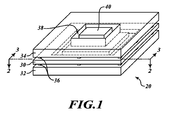
- FIGURE 1 is a perspective view of a sensor package formed in accordance with an embodiment of the present invention.
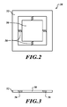
- FIGURES 2 and 3 are cross-sectional views of the package shown in FIGURE 1 ;
- FIGURES 4-1 through 4-8 are cross-sectional views of steps of an exemplary process for forming a sensor package in accordance with an embodiment of the present invention.
- FIGURES 1-3 show a sensor package 20 formed in accordance with an embodiment of the present invention.
- the sensor package 20 includes an isolation layer 30, a sensor device 40 mounted to the isolation layer 30, and upper and lower substrate sections 32, 34 that are mounted to the isolation layer 30 using stud bump 36, such as gold stud bumps (GSBs) or physically comparable stud bumps.
- the upper substrate section (hereinafter “stop ring”) 34 includes a hole 38 for receiving the sensor device 40 but not a raft 50 that is used to support the sensor device 40.
- the isolator layer 30 includes a raft (a center isolation bond pad) 50 connected to a support structure (i.e., stop ring) 52 via springs 56 formed into the material of the isolation layer 30.
- a support structure i.e., stop ring
- Other support structures are possible, including multiple isolation bond pads or a support "ring” divided into many discrete sections.
- the isolator layer 30 is formed by a deep reactive ion etching (DRIE) process.
- DRIE deep reactive ion etching
- the sections 32, 34 and the isolation layer 30 are enclosed within a ceramic, plastic, and/or alumina package that encloses and protects the sensor device 40.
- the stop ring 34 is formed of any suitable material (e.g., metal, silicon, or glass).
- the inner hole 38 is smaller than the raft 50, thus allowing the stop ring 34 to interfere with undesired movements of the raft 50.
- the stop ring includes fingers (not shown) that reach over the raft or the stop ring is formed using multiple separate pieces.
- the sensor device 40 is any sensor requiring a firm mounting, which does not induce stress due to coefficient of thermal expansion (CTE) mismatch and external forces on the package 20.
- the sensor device 40 is an accelerometer, a gyro, a pressure sensor, or other sensing device.
- the stud bumps 36 compress in proportion to force applied.
- the stud bumps 36 get progressively harder to compress as they are crushed and do provide a small spring-back force.
- the stud bumps 36 adhere to metallized portions of the various surfaces. Metallizations are not applied where there is a desire to not have surface-to-bump bonding.
- FIGURES 4-1 through 4-8 show steps of a process for making a sensor package, such as that shown in FIGURE 1 .
- an isolation layer 100 is etched to form a support ring 102, springs 104, and a raft 106.
- stud bumps 110 are bonded to the raft 106 and the support ring 102 using previously applied metallized pads. At this point, the stud bumps 110 are not compressed.
- a stop ring 114 having a hole 116 is compressed to the stud bumps 110, thereby causing them to compress and causing the stud bumps 110 to bond to previously applied metallizations located on the support ring 102 and raft 106. Only the stud bumps 110 bonded to the support ring 102 bond to previously applied metallizations on the stop ring 114.
- the raft 106 is further compressed into the stop ring 114, causing further compression of the raft stud bumps 110.
- This can be done a number of ways, such as flipping the assembly and applying a force only to the raft 106 or applying force to the stop ring 114 while the raft 106 makes contact with a pedestal (as shown).
- stud bumps 122 are added to a base substrate 120 in order to match those on the isolation layer 100.
- the stud bumps 122 are added onto previously applied metallized pads.
- the base substrate 120 is bonded to the isolation layer 100. Because of the spring 104, the stud bumps 122 that are under the support ring 102 become compressed. The raft 106 does not include any metallization on a bottom surface, thereby ensuring no bond occurs with the stud bumps 122.
- stud bumps 130 are applied to a top of the raft 106 through the hole 116 over previously applied metallized pad(s).
- the bumps 130 are applied when the bumps 110 are applied or are attached to a mechanism (i.e., sensor) 136 before the mechanism 136 is attached to the raft 106.
- a force is applied to the mechanism 136 located over the stud bumps 130 on top of the raft 106, thereby causing the mechanism 136 to bond to the stud bumps 130 while depressing the stud bumps 122 under the raft 106.
- the springs 104 cause the raft 106 to return to a null position.
- shock gaps 140 are formed between the raft 106 and the stud bumps 122 and between the stud bumps 122 on the raft 106 and the stop ring 114.
- the isolation raft 106 with the mechanism 136 floats in neutral position with small gaps 140 to limit movement due to shock/vibration, thereby preventing breakage of the springs 104 during excessive shock events.
- steps 1, 2, and 3 are skipped. Only the isolator is bonded to the substrate (no stop ring in this case). Force used to bond mechanism to isolation raft will compress bumps beneath. This will reduce the travel of the isolator during bonding so springs do not break, and after bond there will be a small gap between isolator and substrate.
Landscapes
- Health & Medical Sciences (AREA)
- General Health & Medical Sciences (AREA)
- Toxicology (AREA)
- Engineering & Computer Science (AREA)
- Computer Hardware Design (AREA)
- Microelectronics & Electronic Packaging (AREA)
- Pressure Sensors (AREA)
- Gyroscopes (AREA)
- Force Measurement Appropriate To Specific Purposes (AREA)
Applications Claiming Priority (1)
| Application Number | Priority Date | Filing Date | Title |
|---|---|---|---|
| US13/440,931 US20130264755A1 (en) | 2012-04-05 | 2012-04-05 | Methods and systems for limiting sensor motion |
Publications (2)
| Publication Number | Publication Date |
|---|---|
| EP2647594A2 true EP2647594A2 (fr) | 2013-10-09 |
| EP2647594A3 EP2647594A3 (fr) | 2014-01-22 |
Family
ID=47748400
Family Applications (1)
| Application Number | Title | Priority Date | Filing Date |
|---|---|---|---|
| EP13152435.7A Withdrawn EP2647594A3 (fr) | 2012-04-05 | 2013-01-23 | Procédés et systèmes permettant de limiter le mouvement du capteur |
Country Status (2)
| Country | Link |
|---|---|
| US (1) | US20130264755A1 (fr) |
| EP (1) | EP2647594A3 (fr) |
Cited By (6)
| Publication number | Priority date | Publication date | Assignee | Title |
|---|---|---|---|---|
| EP2871456A1 (fr) * | 2013-11-06 | 2015-05-13 | Sensirion AG | Capteur de pression |
| US9958349B2 (en) | 2015-04-02 | 2018-05-01 | Invensense, Inc. | Pressure sensor |
| US10161817B2 (en) | 2013-11-06 | 2018-12-25 | Invensense, Inc. | Reduced stress pressure sensor |
| CN109458430A (zh) * | 2018-11-27 | 2019-03-12 | 中国舰船研究设计中心 | 基于质量、调谐、混抵效应的浮伐隔振系统优化设计方法 |
| US11225409B2 (en) | 2018-09-17 | 2022-01-18 | Invensense, Inc. | Sensor with integrated heater |
| US11326972B2 (en) | 2019-05-17 | 2022-05-10 | Invensense, Inc. | Pressure sensor with improve hermeticity |
Families Citing this family (5)
| Publication number | Priority date | Publication date | Assignee | Title |
|---|---|---|---|---|
| US10196259B2 (en) | 2015-12-30 | 2019-02-05 | Mems Drive, Inc. | MEMS actuator structures resistant to shock |
| US10322925B2 (en) * | 2015-12-30 | 2019-06-18 | Mems Drive, Inc. | Shock caging features for MEMS actuator structures |
| JP2019522570A (ja) | 2016-05-26 | 2019-08-15 | メムズ ドライブ インク. | Memsアクチュエータ構造の為の衝撃ケージング機構 |
| EP3444609A1 (fr) | 2017-08-14 | 2019-02-20 | Sensirion AG | Mesurage de concentrations d'un gaz cible |
| GB2575694A (en) | 2018-07-20 | 2020-01-22 | Atlantic Inertial Systems Ltd | Sensor packages |
Family Cites Families (24)
| Publication number | Priority date | Publication date | Assignee | Title |
|---|---|---|---|---|
| US6040625A (en) * | 1997-09-25 | 2000-03-21 | I/O Sensors, Inc. | Sensor package arrangement |
| US6937479B2 (en) * | 2001-08-21 | 2005-08-30 | The Charles Stark Draper Laboratory, Inc. | Sensor isolation system |
| US7463125B2 (en) * | 2002-09-24 | 2008-12-09 | Maxim Integrated Products, Inc. | Microrelays and microrelay fabrication and operating methods |
| US6733144B2 (en) * | 2002-09-27 | 2004-05-11 | Intel Corporation | Shock protectors for micro-mechanical systems |
| US20040147056A1 (en) * | 2003-01-29 | 2004-07-29 | Mckinnell James C. | Micro-fabricated device and method of making |
| US8189300B1 (en) * | 2003-05-15 | 2012-05-29 | Wayne Allen Bonin | Multi-layer capacitive transducer with mult-dimension operation |
| JP4134853B2 (ja) * | 2003-09-05 | 2008-08-20 | 株式会社デンソー | 容量式力学量センサ装置 |
| US7458263B2 (en) * | 2003-10-20 | 2008-12-02 | Invensense Inc. | Method of making an X-Y axis dual-mass tuning fork gyroscope with vertically integrated electronics and wafer-scale hermetic packaging |
| JP2006084219A (ja) * | 2004-09-14 | 2006-03-30 | Hosiden Corp | 加速度センサ |
| US7880565B2 (en) * | 2005-08-03 | 2011-02-01 | Kolo Technologies, Inc. | Micro-electro-mechanical transducer having a surface plate |
| US20070246665A1 (en) * | 2006-04-20 | 2007-10-25 | Lafond Peter H | Mechanical isolation for mems devices |
| DE102006022807A1 (de) * | 2006-05-16 | 2007-11-22 | Robert Bosch Gmbh | Chipgehäuse mit reduzierter Schwingungseinkopplung |
| US8049326B2 (en) * | 2007-06-07 | 2011-11-01 | The Regents Of The University Of Michigan | Environment-resistant module, micropackage and methods of manufacturing same |
| US7830003B2 (en) * | 2007-12-27 | 2010-11-09 | Honeywell International, Inc. | Mechanical isolation for MEMS devices |
| US8467559B2 (en) * | 2008-02-20 | 2013-06-18 | Shandong Gettop Acoustic Co., Ltd. | Silicon microphone without dedicated backplate |
| DE102009000574B4 (de) * | 2009-02-03 | 2017-07-27 | Robert Bosch Gmbh | Sensorvorrichtung |
| US8614491B2 (en) * | 2009-04-07 | 2013-12-24 | Honeywell International Inc. | Package interface plate for package isolation structures |
| US10040681B2 (en) * | 2009-08-28 | 2018-08-07 | Miradia Inc. | Method and system for MEMS devices |
| US9227835B2 (en) * | 2010-11-23 | 2016-01-05 | Honeywell International Inc. | Vibration isolation interposer die |
| DE102011003195B4 (de) * | 2011-01-26 | 2019-01-10 | Robert Bosch Gmbh | Bauteil und Verfahren zum Herstellen eines Bauteils |
| US8981497B2 (en) * | 2011-07-19 | 2015-03-17 | Xintec Inc. | Chip package structure and method for forming the same |
| US9778039B2 (en) * | 2011-10-31 | 2017-10-03 | The Regents Of The University Of Michigan | Microsystem device and methods for fabricating the same |
| US8896074B2 (en) * | 2012-01-26 | 2014-11-25 | The Charles Stark Draper Laboratory, Inc. | MEMS vibration isolation system and method |
| US9187313B2 (en) * | 2012-06-26 | 2015-11-17 | Honeywell International Inc. | Anodically bonded strain isolator |
-
2012
- 2012-04-05 US US13/440,931 patent/US20130264755A1/en not_active Abandoned
-
2013
- 2013-01-23 EP EP13152435.7A patent/EP2647594A3/fr not_active Withdrawn
Non-Patent Citations (1)
| Title |
|---|
| None |
Cited By (10)
| Publication number | Priority date | Publication date | Assignee | Title |
|---|---|---|---|---|
| EP2871456A1 (fr) * | 2013-11-06 | 2015-05-13 | Sensirion AG | Capteur de pression |
| CN104634501A (zh) * | 2013-11-06 | 2015-05-20 | 盛思锐股份公司 | 压力传感器 |
| US10161817B2 (en) | 2013-11-06 | 2018-12-25 | Invensense, Inc. | Reduced stress pressure sensor |
| CN104634501B (zh) * | 2013-11-06 | 2019-02-15 | 应美盛股份有限公司 | 压力传感器 |
| US10816422B2 (en) | 2013-11-06 | 2020-10-27 | Invensense, Inc. | Pressure sensor |
| US9958349B2 (en) | 2015-04-02 | 2018-05-01 | Invensense, Inc. | Pressure sensor |
| US10712218B2 (en) | 2015-04-02 | 2020-07-14 | Invensense, Inc. | Pressure sensor |
| US11225409B2 (en) | 2018-09-17 | 2022-01-18 | Invensense, Inc. | Sensor with integrated heater |
| CN109458430A (zh) * | 2018-11-27 | 2019-03-12 | 中国舰船研究设计中心 | 基于质量、调谐、混抵效应的浮伐隔振系统优化设计方法 |
| US11326972B2 (en) | 2019-05-17 | 2022-05-10 | Invensense, Inc. | Pressure sensor with improve hermeticity |
Also Published As
| Publication number | Publication date |
|---|---|
| EP2647594A3 (fr) | 2014-01-22 |
| US20130264755A1 (en) | 2013-10-10 |
Similar Documents
| Publication | Publication Date | Title |
|---|---|---|
| EP2647594A2 (fr) | Procédés et systèmes permettant de limiter le mouvement du capteur | |
| US7571647B2 (en) | Package structure for an acceleration sensor | |
| EP3094950B1 (fr) | Détecteurs de force pour mems à encapsulation sur tranche, miniaturisés et robustes | |
| US20130026655A1 (en) | Chip package structure and method of manufacturing the same | |
| EP2915778B1 (fr) | Isolateur de contrainte lié de façon anodique | |
| US20150307344A1 (en) | Sensor apparatus and method for producing a sensor apparatus | |
| EP1725495A1 (fr) | Dispositif a systeme microelectromecanique (mems) relie a une puce a protuberances | |
| JP5978170B2 (ja) | トランスファーモールド型センサ装置 | |
| EP3176557A1 (fr) | Capteur de pression avec protection contre la surpression pour grandes échelles de surpression à l'intervalle d'opération | |
| US10126183B2 (en) | Actuator for force sensor and method of assembling a force-sensing system | |
| EP1860061B1 (fr) | Isolation de contraintes mécaniques intégrée au niveau de la puce pour un dispositif MEMS | |
| EP2455968A1 (fr) | Interconnexion 3D fabriquée par lots | |
| US20200309615A1 (en) | Force attenuator for force sensor | |
| EP2006248B1 (fr) | Isolateur de contrainte monté sur une puce | |
| CN100555607C (zh) | 半导体器件及其制造方法以及在其中所使用的粘接材料及其制造方法 | |
| JP2018147995A (ja) | 半導体装置およびその製造方法 | |
| WO2007130706A2 (fr) | ensemble électronique et SA méthode de réalisation | |
| JP4613958B2 (ja) | 電子部品の製造方法及び電子部品 | |
| CN105189337B (zh) | 微机电装置和制造方法 | |
| JP5227071B2 (ja) | 半導体素子の実装方法 | |
| JP2007043017A (ja) | 半導体センサ装置 | |
| US11142453B2 (en) | MEMS device stress-reducing structure | |
| FI128296B (en) | Semiconductor Packaging and Method of Manufacturing a Semiconductor Packaging | |
| JP4844118B2 (ja) | センサモジュールおよびその製造方法 | |
| CN118706112A (zh) | 一种mems惯性器件敏感结构及其制作方法 |
Legal Events
| Date | Code | Title | Description |
|---|---|---|---|
| PUAI | Public reference made under article 153(3) epc to a published international application that has entered the european phase |
Free format text: ORIGINAL CODE: 0009012 |
|
| 17P | Request for examination filed |
Effective date: 20130123 |
|
| AK | Designated contracting states |
Kind code of ref document: A2 Designated state(s): AL AT BE BG CH CY CZ DE DK EE ES FI FR GB GR HR HU IE IS IT LI LT LU LV MC MK MT NL NO PL PT RO RS SE SI SK SM TR |
|
| AX | Request for extension of the european patent |
Extension state: BA ME |
|
| PUAL | Search report despatched |
Free format text: ORIGINAL CODE: 0009013 |
|
| AK | Designated contracting states |
Kind code of ref document: A3 Designated state(s): AL AT BE BG CH CY CZ DE DK EE ES FI FR GB GR HR HU IE IS IT LI LT LU LV MC MK MT NL NO PL PT RO RS SE SI SK SM TR |
|
| AX | Request for extension of the european patent |
Extension state: BA ME |
|
| RIC1 | Information provided on ipc code assigned before grant |
Ipc: B81B 7/00 20060101AFI20131217BHEP |
|
| 17Q | First examination report despatched |
Effective date: 20140311 |
|
| STAA | Information on the status of an ep patent application or granted ep patent |
Free format text: STATUS: THE APPLICATION IS DEEMED TO BE WITHDRAWN |
|
| 18D | Application deemed to be withdrawn |
Effective date: 20140722 |