EP2650112B1 - Guide d'onde optique de biopolymère et procédé de fabrication de celui-ci - Google Patents
Guide d'onde optique de biopolymère et procédé de fabrication de celui-ci Download PDFInfo
- Publication number
- EP2650112B1 EP2650112B1 EP13156523.6A EP13156523A EP2650112B1 EP 2650112 B1 EP2650112 B1 EP 2650112B1 EP 13156523 A EP13156523 A EP 13156523A EP 2650112 B1 EP2650112 B1 EP 2650112B1
- Authority
- EP
- European Patent Office
- Prior art keywords
- biopolymer
- silk
- nanopatterned
- diffraction grating
- optical
- Prior art date
- Legal status (The legal status is an assumption and is not a legal conclusion. Google has not performed a legal analysis and makes no representation as to the accuracy of the status listed.)
- Active
Links
Images






Classifications
-
- B—PERFORMING OPERATIONS; TRANSPORTING
- B29—WORKING OF PLASTICS; WORKING OF SUBSTANCES IN A PLASTIC STATE IN GENERAL
- B29D—PRODUCING PARTICULAR ARTICLES FROM PLASTICS OR FROM SUBSTANCES IN A PLASTIC STATE
- B29D11/00—Producing optical elements, e.g. lenses or prisms
-
- G—PHYSICS
- G02—OPTICS
- G02B—OPTICAL ELEMENTS, SYSTEMS OR APPARATUS
- G02B1/00—Optical elements characterised by the material of which they are made; Optical coatings for optical elements
- G02B1/04—Optical elements characterised by the material of which they are made; Optical coatings for optical elements made of organic materials, e.g. plastics
-
- Y—GENERAL TAGGING OF NEW TECHNOLOGICAL DEVELOPMENTS; GENERAL TAGGING OF CROSS-SECTIONAL TECHNOLOGIES SPANNING OVER SEVERAL SECTIONS OF THE IPC; TECHNICAL SUBJECTS COVERED BY FORMER USPC CROSS-REFERENCE ART COLLECTIONS [XRACs] AND DIGESTS
- Y10—TECHNICAL SUBJECTS COVERED BY FORMER USPC
- Y10T—TECHNICAL SUBJECTS COVERED BY FORMER US CLASSIFICATION
- Y10T428/00—Stock material or miscellaneous articles
- Y10T428/24—Structurally defined web or sheet [e.g., overall dimension, etc.]
- Y10T428/24479—Structurally defined web or sheet [e.g., overall dimension, etc.] including variation in thickness
Definitions
- the present invention is directed to nanopatterned biopolymer optical devices, and methods for manufacturing such devices.
- optics The field of optics is well established. Some subfields of optics include diffractive optics, micro-optics, photonics and guided wave optics. Various optical devices have been fabricated in these and other subfields of optics for research and commercial application. For example, common optical devices include diffraction gratings, photonic crystals, optofluidic devices, waveguides, and the like.
- optical devices are fabricated using various methods depending on the application and optical characteristics desired.
- these optical devices, and the fabrication methods employed in their manufacture generally involve significant use of non-biodegradable materials.
- non-biodegradable materials For example, glass, fused silica, and plastic are commonly used in optical devices.
- Such materials are not biodegradable and remain in the environment for extended periods of time after the optical devices are removed from service and discarded.
- some of the materials can be recycled and reused.
- recycling also requires expenditures of natural resources, and adds to the environmental costs associated with such materials.
- JP2001147301A discloses an optical grating made by spin-coating a 10% aqueous silk fibroin solution on a quartz plate and subsequent laser irradiation.
- objects of the present invention are to provide various novel biopolymer optical devices and methods for manufacturing such optical devices that may be used in various applications.
- One aspect of the present invention is to provide nanopatterned biopolymer optical devices.
- Another aspect of the present invention is to provide a method for manufacturing such nanopatterned biopolymer optical devices.
- One advantage of the present invention is in providing optical devices that minimize the negative impact to the environment.
- Another advantage of the present invention is in providing optical devices that are biocompatible.
- Yet another advantage of the present invention is in providing optical devices that have additional functional features that are not provided by conventional optical devices.
- Silk-based materials achieve their impressive mechanical properties with natural physical crosslinks of thermodynamically stable protein secondary structures also known as beta sheets ( ⁇ -sheets). Thus, no exogenous crosslinking reactions or post-processing crosslinking is required to stabilize the materials.
- the presence of diverse amino acid side chain chemistries on silk protein chains facilitates coupling chemistry to functionalize silks, such as with cytokines, morphogens, and cell binding domains.
- biopolymer or synthetic polymer While no other biopolymer or synthetic polymer can match the range of features outlined above for silk, the inventors of the present invention have identified some other polymers that exhibit various properties similar or analogous to silk.
- other natural biopolymers including chitosan, collagen, gelatin, agarose, chitin, polyhydroxyalkanoates, pullan, starch (amylose amylopectin), cellulose, hyaluronic acid, and related biopolymers, or a combination thereof, have been identified.
- the present invention provides various novel nanopatterned biopolymer optical devices and methods for manufacturing such devices.
- one method of manufacturing a nanopatterned biopolymer optical device includes providing a biopolymer, processing the biopolymer to yield a biopolymer matrix solution, providing a substrate with a nanopatterned surface, casting the biopolymer matrix solution on the nanopatterned surface of the substrate, and drying the biopolymer matrix solution to form a solidified biopolymer film on the substrate.
- the solidified biopolymer film includes a nanopattern on its surface.
- the method also includes optionally annealing the solidified biopolymer film and further drying the annealed biopolymer film.
- the optional annealing of the solidified biopolymer film may be performed in a vacuum environment, in a water vapor environment, or in a combination of both environments.
- the substrate and the manufactured biopolymer optical device may be a lens, a microlens array, an optical grating, a pattern generator, or a beam reshaper.
- the biopolymer is silk
- the biopolymer matrix solution is an aqueous silk fibroin solution having approximately 1.0 wt % to 30 wt % silk, inclusive, such as an aqueous silk fibroin solution having approximately 8.0 wt% silk.
- other embodiments may utilize different percent weight solutions to optimize flexibility or strength of the resultant nanopatterned biopolymer optical device, depending on the application, while maintaining the desired optical functions.
- the biopolymer may be chitosan, collagen, gelatin, agarose, chitin, polyhydroxyalkanoates, pullan, starch (amylose amylopectin), cellulose, hyaluronic acid, and related biopolymers, or a combination thereof.
- the method of manufacturing a nanopatterned biopolymer optical device further includes embedding an organic material in the solidified biopolymer film, and/or adding an organic material into the biopolymer matrix solution.
- the organic material may be red blood cells, horseradish peroxidase, or phenolsulfonphthalein, or a combination of these organic materials.
- the organic material may also be a nucleic acid, a dye, a cell, an antibody, enzymes, for example, peroxidase, lipase, amylose, organophosphate dehydrogenase, ligases, restriction endonucleases, ribonucleases, DNA polymerases, glucose oxidase, laccase, cells, viruses, proteins, peptides, small molecules, drugs, dyes, amino acids, vitamins, antixoxidants, DNA, RNA, RNAi, lipids, nucleotides, aptamers, carbohydrates, chromophores, light emitting organic compounds such as luciferin, carotenes and light emitting inorganic compounds, chemical dyes, antibiotics, antifungals, antivirals, light harvesting compounds such as chlorophyll, bacteriorhodopsin, protorhodopsin, and porphyrins and related electronically active compounds, or a combination thereof.
- enzymes for example, peroxidase, lipa
- a nanopatterned biopolymer optical device that includes a solidified biopolymer film with a surface having a nanopattern thereon.
- the biopolymer optical device may be an optical grating, a lens, a microlens array, a pattern generator, or a beam reshaper.
- the invention also relates to a method of manufacturing a nanopatterned biopolymer optical device comprising:
- the method further comprises:
- the method further comprises annealing said solidified biopolymer film, wherein said annealing of said solidified biopolymer film is optionally performed in at least one of a vacuum environment and a water vapor environment.
- said substrate is a template for an optical device.
- said substrate is a template for at least one of a lens, a microlens array, an optical grating, a pattern generator, and a beam reshaper.
- said biopolymer is silk.
- said biopolymer matrix solution is an aqueous silk fibroin solution having approximately 1.0 wt % to 30 wt % silk, inclusive. Ideally, said aqueous silk fibroin solution has approximately 8.0 wt % silk.
- said biopolymer is selected from a group consisting of chitosan, collagen, gelatin, agarose, chitin, polyhydroxyalkanoates, pullan, starch (amylose amylopectin), cellulose, hyaluronic acid, and related biopolymers, or a combination thereof.
- the method further comprises embedding an organic material in said solidified biopolymer film.
- the method further comprises adding an organic material into said biopolymer matrix solution.
- said organic material is selected from a group consisting of red blood cells, horseradish peroxidase, and phenolsulfonphthalein, or a combination thereof.
- said organic material is selected from a group consisting of nucleic acid, a dye, a cell, an antibody, enzymes, for example, peroxidase, lipase, amylose, organophosphate dehydrogenase, ligases, restriction endonucleases, ribonucleases, DNA polymerases, glucose oxidase, laccase, cells, viruses, proteins, peptides, small molecules, drugs, dyes, amino acids, vitamins, antixoxidants, DNA, RNA, RNAi, lipids, nucleotides, aptamers, carbohydrates, chromophores, light emitting organic compounds such as luciferin, carotenes and light emitting inorganic compounds, chemical dyes, antibiotics, antifungals, antivirals, light harvesting compounds such as chlorophyll, bacteriorhodopsin, protorhodopsin, and porphyrins and related electronically active compounds, or a combination thereof.
- enzymes for example, peroxidas
- the method further comprises machining said nanopattern on said substrate.
- said machining of said nanopattern on said substrate is performed using a laser.
- said machining is performed by femtosecond laser pulses generated by said laser.
- the invention also relates to a nanopatterned biopolymer optical device comprising a solidified biopolymer film with a surface having a nanopattern thereon.
- said biopolymer optical device is at least one of a lens, a microlens array, an optical grating, a pattern generator, and a beam reshaper.
- said solidified polymer film is silk.
- said solidified biopolymer film is selected from a group consisting of chitosan, collagen, gelatin, agarose, chitin, polyhydroxyalkanoates, pullan, starch (amylose amylopectin), cellulose, hyaluronic acid, and related biopolymers, or a combination thereof.
- the nanopatterned biopolymer optical device further comprises an organic material embedded in said solidified biopolymer film.
- said organic material is selected from a group consisting of red blood cells, horseradish peroxidase, and phenolsulfonphthalein, or a combination thereof.
- said organic material is selected from a group consisting of nucleic acid, a dye, a cell, an antibody, enzymes, for example, peroxidase, lipase, amylose, organophosphate dehydrogenase, ligases, restriction endonucleases, ribonucleases, DNA polymerases, glucose oxidase, laccase, cells, viruses, proteins, peptides, small molecules, drugs, dyes, amino acids, vitamins, antixoxidants, DNA, RNA, RNAi, lipids, nucleotides, aptamers, carbohydrates, chromophores, light emitting organic compounds such as luciferin, carotenes and light emitting inorganic compounds, chemical dyes, antibiotics, antifungals, antivirals, light harvesting compounds such as chlorophyll, bacteriorhodopsin, protorhodopsin, and porphyrins and related electronically active compounds, or a combination thereof.
- enzymes for example, peroxidas
- the nanopatterned biopolymer optical devices in accordance with the present invention have been fabricated using a biopolymer such as silk.
- the silk utilized was silkworm silk.
- silks including spider silk, transgenic silks, and genetically engineered silks, variants and combinations thereof and others, that may alternatively be used in accordance with the present invention to obtain a nanopatterned biopolymer optical device.
- biodegradable polymers may be used instead of silk.
- additional biopolymers such as chitosan, exhibit desirable mechanical properties, can be processed in water, and form generally clear films for optical applications.
- Other biopolymers such as chitosan, collagen, gelatin, agarose, chitin, polyhydroxyalkanoates, pullan, starch (amylose amylopectin), cellulose, hyaluronic acid, and related biopolymers, or a combination thereof, may alternatively be utilized in specific applications, and synthetic biodegradable polymers such as polylactic acid, polyglycolic acid, polyhydroxyalkanoates and related copolymers may also be selectively used. Some of these polymers are not as easily processable in water. Nonetheless, such polymers may be used by themselves, or in combinations with silks, and may be used in particular biopolymer optical devices.
- nanopatterned refers to very small patterning that is provided on a surface of the biopolymer optical device.
- the patterning has structural features whose size can be appropriately measured on a nanometer scale (that is, 10 -9 meters), for example, sizes ranging from 100 nm to few microns.
- the biopolymer optical devices of the present invention may incorporate various different optical devices such as lenses, diffraction gratings, photonic crystals, waveguides, and the like.
- FIG. 1 is a schematic illustration of a flow diagram 10 showing a method of manufacturing a nanopatterned biopolymer optical device in accordance with one embodiment of the present invention.
- a biopolymer matrix solution is provided in step 11, the process proceeds to step 16 described below. Otherwise, a biopolymer is provided in step 12.
- the biopolymer may be attained by extracting sericin from the cocoons of Bombyx mori .
- the provided biopolymer is processed to yield a biopolymer matrix solution in step 14.
- the biopolymer matrix solution is an aqueous matrix solution.
- different solvents other than water, or a combination of water and other solvents may be used, depending on the biopolymer used.
- an aqueous silk fibroin solution is processed in step 14, for example, 8.0 wt %, which is then used to manufacture the nanopatterned biopolymer optical device.
- the solution concentrations may also be varied from very dilute (approximately 1 wt %) to very high (up to 30 wt %) using either dilution or concentration, for example, via osmotic stress or drying techniques.
- other embodiments may utilize different percent weight solutions to optimize flexibility or strength of the resultant nanopatterned biopolymer optical device, depending on the application. Production of aqueous silk fibroin solution is described in detail in WIPO Publication Number WO 2005/012606 entitled "Concentrated Aqueous Silk Fibroin Solution and Uses Thereof".
- a substrate is provided in step 16 to serve as a mold in manufacturing the biopolymer optical device.
- a surface of the substrate has the desired characteristic features to be formed on the biopolymer optical device.
- the substrate may be an appropriate nanopattern on a surface of the optical device and may be an optical device such as a nanopatterned optical grating, depending on the optical features desired for the biopolymer optical device being manufactured.
- the aqueous biopolymer matrix solution is then cast on the substrate in step 18.
- the aqueous biopolymer matrix solution is then dried in step 20 to transition the aqueous biopolymer matrix solution to the solid phase.
- the aqueous biopolymer matrix solution may be dried for a period of time such as 24 hours, and may optionally be subjected to low heat to expedite drying of the aqueous biopolymer matrix solution.
- a solidified biopolymer film is formed on the surface of the substrate. The thickness of the biopolymer film depends on the volume of the biopolymer matrix solution applied to the substrate.
- the solidified biopolymer film may be optionally annealed in step 22.
- This annealing step is preferably performed within a water vapor environment, such as in a chamber filled with water vapor, for different periods of time depending on the material properties desired. Typical annealing time periods may range from between two hours to two days, for example, and may also be performed in a vacuum environment.
- the annealed biopolymer film is then removed from the substrate in step 24 and allowed to dry further in step 26, thereby resulting in a biopolymer optical device.
- the annealed films manufactured in the above-described manner have a functional optical surface that matches the surface provided on the substrate.
- the annealed film can then be used as a nanopatterned biopolymer optical device in accordance with the present invention.
- the film properties such as thickness and biopolymer content, as well as optical features, may be altered based on the concentration of fibroin used in the process, the volume of the aqueous silk fibroin solution deposited, and the post deposition process for drying the cast solution to lock in the structure. Accurate control of these parameters is desirable to ensure the optical quality of the resultant biopolymer optical device and to maintain various characteristics of the biopolymer optical device, such as transparency, structural rigidity, and flexibility.
- additives to the biopolymer matrix solution may be used to alter features of the biopolymer optical device such as morphology, stability, and the like, as known with polyethylene glycols, collagens, and the like.
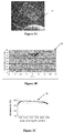
- FIG. 3A illustrates the unpatterned biopolymer film 34 manufactured and characterized.
- the characterization of the unpatterned silk film 34 is shown in graph 36 of Figure 3B , which clearly demonstrates the prism coupled angular dependence of the reflectivity.
- the oscillations in graph 36 are due to coupling into guided waves, demonstrating the use of silk as a waveguide material.
- FIG. 3C is a graph 38 that illustrates the measured transmission of light through the silk film 34 in various wavelengths. Transmission measurements indicate that the unpatterned silk film 34 was highly transparent across the visible spectrum. For comparison, similar thickness films were also cast in collagen, and polydimethylsiloxane (PDMS). The free-standing structural stability was found to be inferior, and the resultant biopolymer optical device was not self-supporting when implemented as a thin film. However, such biopolymers may be used in an application if structural stability is deemed to be not as important.
- PDMS polydimethylsiloxane
- nanopatterned biopolymer optical devices were successfully manufactured using the above-described method of the present invention using silk fibroin solution. These devices included lenses, microlens arrays, optical gratings, pattern generators and beam reshapers.
- the aqueous solution of silk fibroin was cast onto specific substrates with patterns thereon. The substrate surfaces were coated with TeflonTM to ensure even detachment after the biopolymer matrix solution transitions from the liquid to the solid phase.
- biopolymer casting method of the present invention for forming highly defined nanopatterned structures in biopolymer optical devices was verified by casting diffraction gratings and lenses. Regular patterned features with dimensions down to 210 nm, and localized surface roughness of less than 20 nm, have been attained.
- Such regular patterning of biocompatible materials allows manufacturing of optical devices that can be used to provide photonic bandgaps and manipulate light via an organic, yet mechanically robust optical device. These devices combine the flexibility of embedded optics with the unique versatility of the protein substrate as explained in further detail below. Many advantages are provided by the present invention including combining the organic nature of biopolymers such as silk with the power of diffractive and transmissive optics embedded in an organic matrix to create biologically active optical elements.
- Silk provides a controllably degradable, biocompatible, and structurally strong medium with which to fabricate the optical devices in accordance with the present invention.
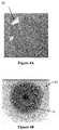
- Figure 4A is a photograph showing a nanopatterned biopolymer focusing lens 40 that was manufactured using the method described above with an aqueous silk fibroin solution.
- the biopolymer focusing lens 40 has a diameter of less than 1 centimeter and has nanopatterned concentric rings formed on its surface.
- Figure 4B is a microscopic image 42 of the biopolymer focusing lens 40 shown in Figure 4A .
- the microscopic image 42 clearly shows the nanopatterned concentric rings 44 on the biopolymer focusing lens.
- Figure 5 shows a photograph image 50 of lettering "Tufts" as seen through the nanopatterned focusing lens 40 of Figure 4A . This photograph clearly illustrates the optical applicability of optical devices made of biopolymers that are manufactured in accordance with the method of the present invention.
- nanopatterned biopolymer optical devices were manufactured by casting the aqueous silk fibroin solutions on microlens arrays and on other pattern generators.
- the aqueous silk fibroin solution was cast on various patterned surfaces of optical elements, left to solidify, and subsequently annealed in accordance with the method described above with regard to Figure 1 .
- Figures 6A and 6B are photographs of a lens array 60 manufactured in accordance with the present invention using aqueous silk fibroin solution.
- the lens array 60 was cast on a polycarbonate film from Digital Optics Corporation.
- the obtained silk lens array 60 is approximately 1 cm 2 in size and is patterned with 12x12 lenses 62 thereon.
- the lenses 62 provided on the lens array 60 demonstrate that accurately patterned biopolymer optical devices can be manufactured by casting a biopolymer matrix solution, such as an aqueous silk fibroin solution, on a substrate that functions as a mold.
- Figure 6B is a photograph of text as seen through the silk lens array 60.
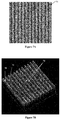
- FIG. 7A is a scanning electron microscope image of a portion of a nanopatterned biopolymer diffraction grating 70 that was manufactured in accordance with the method of Figure 1 by casting an aqueous silk fibroin solution on a holographic diffraction grating with 2,400 lines/mm.
- the resultant biopolymer diffraction grating 70 of silk also has gratings 72 at 2,400 lines/mm.
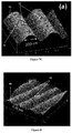
- Figures 7B and 7C are atomic force microscope (AFM), and high-resolution AFM images, respectively, of a portion of the surface of the nanopatterned biopolymer diffraction grating 70.
- the portion of the diffraction grating 70 shown in Figure 7C is approximately 1 ⁇ m 2 .
- the ridges of the grating were approximately 200nm wide and spaced by approximately 200 nm at full width at half maximum (FWHM). The peak to valley height difference of 150 nm was observed.
- nanopatterned biopolymer diffraction grating 70 had highly regular, structured gratings 72 on the nanoscale with remarkably smooth sidewalls 74.
- a topographical evaluation of the surface roughness at the peaks of the gratings 72 and valleys between the gratings 72 revealed surface roughness root mean square (RMS) values below 20 nm while being structurally stable. These values characterize outstanding resolution from optics and materials perspectives.
- RMS root mean square
- the measured roughness of cast silk film on an optically flat surface shows measured root mean squared roughness values between 2.5 and 5 nanometers, which implies a surface roughness easily less than ⁇ /50 at a wavelength of 633 nm.
- Atomic force microscope images of patterned silk diffractive optics show the levels of microfabrication obtainable by casting and lifting silk films off of appropriate molds. The images show definition in the hundreds of nanometer range and the sharpness of the corners indicates the possibility of faithful patterning down to the tens of nanometers.
- Figure 8 is a high-resolution atomic force microscope (AFM) image of a 1 ⁇ m 2 portion of a nanopatterned silk diffraction grating 80 that was also manufactured in accordance with the method of the present invention by casting aqueous silk fibroin solution on an optical diffraction grating having a pitch of 3,600 lines/mm.
- the resultant biopolymer diffraction grating 80 also has 3,600 lines/mm.
- the structured gratings 82 were measured to be 125 nm apart at FWHM with a peak to valley height difference of 60 nm. As can be seen, highly regular structured gratings 82 on the nanoscale were obtained with remarkably smooth sidewalls. Topographic analysis of the surfaces again revealed a surface roughness of less than 20 nanometers RMS.
- diffraction gratings of different line pitches, and different sizes as large as 50 x 50 mm were also manufactured using the method of the present invention.
- diffraction gratings having 600 lines/mm and 1,200 lines/mm were also used to manufacture nanopatterned biopolymer diffraction gratings.
- the resultant nanopatterned biopolymer diffraction gratings were found to reproduce the fine features with a surface smoothness having RMS less than 20 nm while being structurally stable. In certain areas, the smoothness was found to have RMS roughness of less than 10 nm.
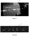
- Figure 9B is another photograph 96 that illustrates diffracted orders from a supercontinuum laser source impinging on a silk diffraction grating with 1,200 lines/mm that was made in accordance with the present invention.
- the diffracted orders were imaged 2 cm from the silk diffraction grating.
- the diffraction efficiency of this grating was found to be 34% in the first order at 633 nm, which compares favorably to conventional transmissive glass gratings.
- the structural stability and the ability to faithfully reproduce nanostructures makes the above-described method an excellent process for manufacturing many different diffractive optical structures or refractive micro and nano-optical structures.
- various optical devices that can be readily manufactured are optical gratings, micro and nano lens arrays as described above, pattern generators, beam diffusers, beam homogenizers or layered diffractive optics, such as photonic crystals or waveguides.
- Transmissive nanopatterned diffractive biopolymer optical devices were made using the method of the present invention described above. These optical devices include silk diffusers, line pattern generators, and cross pattern generators. Such optical devices use appropriately configured wavelength scale surface structuring to create predefined one or two-dimensional light patterns that exploit light interference. Such optical devices made of conventional materials have been applied to imaging, spectroscopy, beam sampling and transformation, and metrology to name a few uses. Extending this approach to control the delivery of light within a biological matrix such as silk biopolymer can provide optimal coupling of photons into a substrate or allow for designed optical discrimination, interface, or readout.
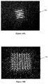
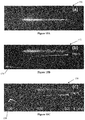
- Figures 10A shows silk optic diffractive grating 100
- Figure 10B shows silk optic diffractive element 104. Both are example embodiments of the present invention and were manufactured in the manner described above. The devices were photographed when a broad white light laser was transmitted through the respective structures.
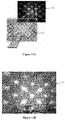
- Figures 11A through 11C each show various far field images photographed after transmitting broadband white light laser through various silk diffractive optical devices. The resulting patterns are multicolored due to the dispersion of the broad supercontinuum laser used to generate the images.
- Figure 11A is a schematic illustration of laser light passed through nanopatterned biopolymer optical device 111 to generate the light pattern shown in photograph 112.
- Figure 11B is a photograph 114 of another pattern generated by laser light passed through another nanopatterned biopolymer optical device.
- Figure 11C is a photograph 116 of still another pattern generated by a white laser light passed through still another nanopatterned biopolymer optical device.
- the nanopatterned biopolymer optical device of Figure 11C is a replica of a diffractive pattern commercially available from Diffractive Optics, Inc. of Charlotte, North Carolina.
- a significant advantage of nanopatterned biopolymer optical devices in accordance with the present invention is the ability to embed optics in entirely organic, biocompatible, and extremely functional substrates, thereby allowing the optics to be biologically active.
- the nanopatterned biopolymer optical devices of the present invention can be biologically activated by embedding organic materials, such as proteins, into the nanopatterned biopolymer optical device.
- the silk diffraction grating described above can be fabricated so that changes can be biologically induced in the grating. This phenomenon alters the diffraction efficiency locally. The variation of the diffracted beams can then function as an indicator of the changes occurring at the biological level.
- Such responsive nanopatterned biopolymer optical devices can be implemented by the addition of nucleic acid, a dye, a cell, an antibody, as described further in Appendix I, enzymes, for example, peroxidase, lipase, amylose, organophosphate dehydrogenase, ligases, restriction endonucleases, ribonucleases, DNA polymerases, glucose oxidase, laccase, cells, viruses, bacterias, proteins, peptides for molecular recognition, small molecules, drugs, dyes, amino acids, vitamins, antixoxidants, plant cells, mammalian cells, and the like, DNA, RNA, RNAi, lipids, nucleotides, aptamers, carbohydrates, optically-active chromophores ncluding beta carotene or porphyrins,, light emitting organic compounds such as luciferin, carotenes and light emitting inorganic compounds, chemical dyes, antibiotics, yeast, antifungals, antivirals,
- Figure 12A shows a scanning electron microscope image of a surface of a silk diffraction grating 120 before surface processing.
- Figure 12B shows a scanning electron microscope image of the surface of the silk diffraction grating 120 after surface processing.
- the surface of the silk diffraction grating 120 shown in Figures 12A and 12B are processed so that binding is obtained selectively on the troughs 124 of the diffraction grating 120, thereby altering the pitch and the resulting optical structure of the diffraction grating 120 as shown in Figure 12B.
- Figure 12A shows that every other trough has been filled with a binding 126.
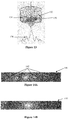
- Figure 13 schematically illustrates a silk diffraction grating 130 having 600 lines/mm exposed to a cellular environment of corneal fibroblast by immersing the silk diffraction grating 130 in a plain buffer solution 132 with corneal fibroblast 134.
- the silk fibroin is a good substrate for the fibroblast cells, which coats the surface of the silk diffraction grating 130 thereby removing (or interfering with) its diffractive properties.
- the gratings that are exposed to an unsuitable environment for coating maintain their diffractive properties.
- the interference can be verified by monitoring the change in the transmission of light through the silk diffraction grating 130 as also schematically illustrated by the graph 136 of Figure 13 .
- Figure 14A is a photograph 140 of the resultant efficient diffraction that occurs when a laser beam is propagated through a nanopatterned silk diffraction grating in a culture dish with the plain buffer solution.
- the resultant diffracted orders 142 are clearly shown in the photograph 140.
- Figure 14B is a photograph 144 of the resultant diffraction when the laser beam is propagated through the same nanopatterned silk diffraction grating in a culture dish with the corneal fibroblast solution.
- the comparative loss of diffraction properties results when the nanopatterned silk diffraction grating is in the presence of the corneal fibroblast that deposits and alters the diffractive order. By examining the grating's diffractive properties, changes in the functionalized detection of the diffraction grating may be demonstrated.
- results of one example experiment are shown in the spectral image photographs of Figures 15A through 15C in which supercontinuum light of 350 nm to more than 1,000 nm was transmitted through a nanopatterned silk diffraction grating in accordance with the present invention.
- the spectral images were taken at a distance of 15 cm from the nanopatterned silk diffraction grating.
- photograph 150 of Figure 15A illustrates the diffracted supercontinuum light when passed through an undoped nanopatterned silk diffraction grating and projected onto a fixed plane.
- Photograph 152 of Figure 15B illustrates the diffracted supercontinuum light when passed through a nanopatterned silk diffraction grating that was activated by embedding it with phenolsulfonphthalein (PSP) and exposed to an acid solution.
- PSP phenolsulfonphthalein
- the measured spectral transmission curve 154 is overlaid to match the diffracted supercontinuum spectrum detected.
- Photograph 156 of Figure 15C illustrates the diffracted supercontinuum when the PSP-embedded nanopatterned silk diffraction grating is exposed to a base solution.
- the measured spectral transmission curve 158 is also overlaid to match the diffracted supercontinuum spectrum detected. As can be seen, more absorbance is exhibited towards the green end (that is, shorter wavelengths) of the spectrum.
- red blood cells were incorporated into a silk diffraction grating in accordance with the present invention that was manufactured as described above with regard to Figure 1 .
- the RBC-silk fibroin solution was prepared by combining 1 ml of an 80% hematocrit human RBC solution and 5 ml of the 8% silk solution. The mixture was cast on a 600 lines/mm optical grating and allowed to dry overnight. The film was removed from the optical grating and annealed for two hours. The grating structure was observed in the resultant RBC-doped silk diffraction grating.
- the RBC-doped silk diffraction grating was then tested to observe the diffraction orders.
- An optical transmission experiment was performed to determine whether hemoglobin (the oxygen-carrying protein contained in RBCs) maintained its activity within the matrix of the silk diffraction grating.
- the results graphs 160 are shown in Figure 16 and indicate the retention of hemoglobin function within the RBC-doped silk diffraction grating.
- the X-axis corresponds to the wavelength (in nm), and the Y-axis indicates the absorbance by the RBC-doped silk diffraction grating.
- HRP horseradish peroxidase
- TMB tetramethylbenzidine
- the oxidation products of TMB yield a characteristic blue color (one-electron oxidation) yield a yellow color (two-electron oxidation).
- the recorded absorption spectra is shown in results graphs 170 of Figure 17 , where the X-axis corresponds to the wavelength (in nm), and the Y-axis indicates the absorbance by the HRP-embedded silk diffraction grating.
- the absorption spectra was recorded in graphs 90 at the initial stages of the reaction at 5, 15, 25, and 35 seconds, immediately after exposing the optical element to TMB.
- an organic pH indicator phenolsulfonphthalein (phenol red)
- phenol red phenolsulfonphthalein
- the resulting diffractive optical structures maintained the functionality of the pH indicator and the optical function of the silk diffraction grating.
- supercontinuum radiation was diffracted through the phenol-red embedded silk diffraction grating.
- the same diffraction grating was then dipped into solutions with different pH levels including 1 mM NaOH, 1 mM HCl, and DI H 2 O.
- FIG. 18 shows a photograph 180 that illustrates other diffractive biopolymer optical devices that have been cast using different materials.
- a chitosan optical device 182 and a collagen optical device 184 have also been manufactured in accordance with the present invention.
- optical diffraction characteristics similar to silk have been observed.
- the present invention provides biodegradable nanopatterned biopolymer optical devices.
- High quality nanopatterned biopolymer optical devices were manufactured that are naturally biocompatible, can be processed in water, and can undergo degradation with controlled lifetimes.
- the nanopatterned biopolymer optical devices of the present invention may also be biologically activated by incorporating small organic materials.
- the small organic materials may be complex proteins such as hemoglobin in the red blood cells and enzymes such as peroxidase.
- the present invention broadens the versatility of optical devices by allowing the direct incorporation of labile biological receptors in the form of peptides, enzymes, cells, antibodies, or related systems, and allows such optical devices to function as biological sensing devices.
- the nanopatterned biopolymer optical devices of the present invention can be readily used in environmental and life sciences where biocompatibility and biodegradability are paramount.
- the nanopatterned biopolymer optical devices as described above can be unobtrusively used to monitor a natural environment such as in the human body and may be implanted in vivo without a need to retrieve the device at a later time.
- the degradation lifetime of the nanopatterned biopolymer optical devices of the present invention can be controlled during the manufacturing process, for example, by controlling the ratio and amount of the solution matrix cast.
- the nanopatterned biopolymer optical devices of the present invention can be dispersed in the environment, again without the need to retrieve them at a later time, thereby providing novel and useful devices for sensing and detection.
- IgG1 Materials - Anti-IL-8 monoclonal antibody (IgG1) was purchased from eBioscience, Inc. human polyclonal antibody IgG and human IgG ELISA Quantitation Kit were purchased from Bethyl Laboratories Inc. All other chemicals used in the study were purchased from Sigma-Aldrich (St. Louis, MO).
- Anti-IL-8 monoclonal antibody (IgG1) - 0.5ml 1 mg/ml IgG1 mixed with 83 ml 6% silk solution make the IgG1 concentration in silk film 0.1 mg/g silk.
- 50 ⁇ l of mixed IgG1 solution was added to a well of 96 well plate which was placed in a fume hood with cover opened overnight. The dried film was either treated or not treated with methanol. For methanol treatment, the wells were immersed in 90% methanol solution for 5 min and dried in the fume hood. All dry 96 well plates were then stored at 4°C, room temperature, and 37°C.
- Antibody measurement Five wells prepared at the same condition were measured for statistic. Pure silk (without antibody) was used as a control.
- ELISA - Polystyrene (96-well) microtitre plate was coated with 100 ⁇ L of antigen antiHuman IgG-affinity at a concentration of 10 ⁇ g/mL prepared in antigen coating buffer (bicarbonate buffer, 50 mM, pH 9.6) and then incubated overnight storage at room temperature. The wells were then washed three times with TBS-T buffer. The unoccupied sites were blocked with 1% BSA in TBS (200 ⁇ L each well) followed by incubation for 30 minutes at room temperature. The wells were then washed three times with TBS-T. The test and control wells were then diluted with 100 ⁇ L of serially diluted serum. Each dilution was in TBS buffer.
Landscapes
- Engineering & Computer Science (AREA)
- Physics & Mathematics (AREA)
- Health & Medical Sciences (AREA)
- General Physics & Mathematics (AREA)
- Optics & Photonics (AREA)
- Manufacturing & Machinery (AREA)
- Ophthalmology & Optometry (AREA)
- Mechanical Engineering (AREA)
- Chemical & Material Sciences (AREA)
- Investigating Or Analysing Materials By Optical Means (AREA)
- Chemical Kinetics & Catalysis (AREA)
- Medicinal Chemistry (AREA)
- Polymers & Plastics (AREA)
- Organic Chemistry (AREA)
- Diffracting Gratings Or Hologram Optical Elements (AREA)
- Moulding By Coating Moulds (AREA)
Claims (1)
- Film de fibroïne de soie, comprenant :au moins un matériau organique inclus dans le film, où le matériau organique est constitué de, ou comprend, un anticorps ou une enzyme ;où l'une des surfaces du film possède une nano-impression sur celle-ci et le film agit comme nano-dispositif biophotonique choisi dans le groupe constitué par les lentilles, les réseaux de microlentilles, les réseaux optiques, les générateurs de mires et les reprofileurs de faisceaux ; etoù le film est formé à partir d'une solution de fibroïne de soie ayant une concentration comprise entre environ 1,0% en poids et environ 30% en poids de soie.
Applications Claiming Priority (3)
| Application Number | Priority Date | Filing Date | Title |
|---|---|---|---|
| US85629706P | 2006-11-03 | 2006-11-03 | |
| US90750207P | 2007-04-05 | 2007-04-05 | |
| EP07873592.5A EP2086749B1 (fr) | 2006-11-03 | 2007-11-05 | Dispositif optique de biopolymère à nanomotifs et procédé de fabrication de celui-ci |
Related Parent Applications (2)
| Application Number | Title | Priority Date | Filing Date |
|---|---|---|---|
| EP07873592.5A Division EP2086749B1 (fr) | 2006-11-03 | 2007-11-05 | Dispositif optique de biopolymère à nanomotifs et procédé de fabrication de celui-ci |
| EP07873592.5 Division | 2007-11-05 |
Publications (3)
| Publication Number | Publication Date |
|---|---|
| EP2650112A2 EP2650112A2 (fr) | 2013-10-16 |
| EP2650112A3 EP2650112A3 (fr) | 2014-01-15 |
| EP2650112B1 true EP2650112B1 (fr) | 2016-08-24 |
Family
ID=39789707
Family Applications (2)
| Application Number | Title | Priority Date | Filing Date |
|---|---|---|---|
| EP13156523.6A Active EP2650112B1 (fr) | 2006-11-03 | 2007-11-05 | Guide d'onde optique de biopolymère et procédé de fabrication de celui-ci |
| EP07873592.5A Active EP2086749B1 (fr) | 2006-11-03 | 2007-11-05 | Dispositif optique de biopolymère à nanomotifs et procédé de fabrication de celui-ci |
Family Applications After (1)
| Application Number | Title | Priority Date | Filing Date |
|---|---|---|---|
| EP07873592.5A Active EP2086749B1 (fr) | 2006-11-03 | 2007-11-05 | Dispositif optique de biopolymère à nanomotifs et procédé de fabrication de celui-ci |
Country Status (5)
| Country | Link |
|---|---|
| US (1) | US9969134B2 (fr) |
| EP (2) | EP2650112B1 (fr) |
| JP (2) | JP2010509645A (fr) |
| CA (1) | CA2704769C (fr) |
| WO (1) | WO2008127404A2 (fr) |
Families Citing this family (75)
| Publication number | Priority date | Publication date | Assignee | Title |
|---|---|---|---|---|
| CA2525994C (fr) * | 2002-06-24 | 2012-10-16 | Tufts University | Biomateriaux a base de soie et leurs methodes d'utilisation |
| WO2004062697A2 (fr) | 2003-01-07 | 2004-07-29 | Tufts University | Matières de fibroïne de soie et utilisation de celles-ci |
| CA2562415C (fr) | 2003-04-10 | 2015-10-27 | Tufts University | Solution aqueuse concentree de fibroine |
| WO2005000483A1 (fr) * | 2003-06-06 | 2005-01-06 | Tufts University | Procede de formation d'enrobages inorganiques |
| KR101368748B1 (ko) | 2004-06-04 | 2014-03-05 | 더 보오드 오브 트러스티스 오브 더 유니버시티 오브 일리노이즈 | 인쇄가능한 반도체소자들의 제조 및 조립방법과 장치 |
| US20100046902A1 (en) | 2006-11-03 | 2010-02-25 | Trustees Of Tufts College | Biopolymer photonic crystals and method of manufacturing the same |
| CA2704768A1 (fr) * | 2006-11-03 | 2008-10-23 | Trustees Of Tufts College | Capteur de biopolymere et procede de fabrication de celui-ci |
| US20100096763A1 (en) * | 2006-11-03 | 2010-04-22 | Trustees Of Tufts College | Biopolymer optofluidic device and method of manufacturing the same |
| EP2650112B1 (fr) | 2006-11-03 | 2016-08-24 | Trustees Of Tufts College | Guide d'onde optique de biopolymère et procédé de fabrication de celui-ci |
| WO2008106485A2 (fr) * | 2007-02-27 | 2008-09-04 | Trustees Of Tufts College | Organes de soie produits par génie tissulaire |
| US8187616B2 (en) | 2007-05-29 | 2012-05-29 | Trustees Of Tufts College | Method for silk fibroin gelation using sonication |
| EP2206017B1 (fr) | 2007-11-05 | 2019-02-20 | Trustees Of Tufts College | Fabrication de structures photoniques de fibroïne de soie par impression par nanocontact |
| CN101970023A (zh) * | 2008-02-07 | 2011-02-09 | 塔夫茨大学信托人 | 三维的丝羟基磷灰石组合物 |
| CA2721961A1 (fr) * | 2008-05-15 | 2009-11-19 | Trustees Of Tufts College | Liberation d'adenosine a base de polymere de soie : potentiel therapeutique pour l'epilepsie |
| EP2307054A4 (fr) * | 2008-06-18 | 2013-02-06 | Tufts College | Produits holographiques comestibles en soie |
| US8501172B2 (en) | 2008-09-26 | 2013-08-06 | Trustees Of Tufts College | pH-induced silk gels and uses thereof |
| US8372726B2 (en) | 2008-10-07 | 2013-02-12 | Mc10, Inc. | Methods and applications of non-planar imaging arrays |
| US8389862B2 (en) | 2008-10-07 | 2013-03-05 | Mc10, Inc. | Extremely stretchable electronics |
| US8097926B2 (en) | 2008-10-07 | 2012-01-17 | Mc10, Inc. | Systems, methods, and devices having stretchable integrated circuitry for sensing and delivering therapy |
| EP2349440B1 (fr) | 2008-10-07 | 2019-08-21 | Mc10, Inc. | Ballonnet de cathéter comportant un circuit intégré étirable et un réseau de détecteurs |
| US8886334B2 (en) | 2008-10-07 | 2014-11-11 | Mc10, Inc. | Systems, methods, and devices using stretchable or flexible electronics for medical applications |
| KR20110094277A (ko) | 2008-10-09 | 2011-08-23 | 트러스티즈 오브 터프츠 칼리지 | 글리세롤을 함유하는 변성 실크 필름 |
| US9308070B2 (en) | 2008-12-15 | 2016-04-12 | Allergan, Inc. | Pliable silk medical device |
| EP2396276B1 (fr) * | 2009-02-12 | 2016-08-31 | Trustees Of Tufts College | Lithographie par nano-impression de structures de fibroïne de soie pour des applications biomédicales et biophotoniques |
| US8420077B2 (en) | 2009-04-20 | 2013-04-16 | Allergan, Inc. | Silk fibroin hydrogels and uses thereof |
| CA2812635A1 (fr) | 2009-07-14 | 2011-01-20 | Trustees Of Tufts College | Systemes de materiau de soie electrofilee pour cicatrisation |
| US9016875B2 (en) | 2009-07-20 | 2015-04-28 | Tufts University/Trustees Of Tufts College | All-protein implantable, resorbable reflectors |
| WO2011026101A2 (fr) | 2009-08-31 | 2011-03-03 | Trustees Of Tufts College | Dispositifs à transistor à base de soie |
| CA2775706A1 (fr) | 2009-09-28 | 2011-03-31 | Trustees Of Tufts College | Fibres de soie electrogelifiees etirees et leurs procedes de production |
| JP5730317B2 (ja) | 2009-09-29 | 2015-06-10 | タフツ ユニバーシティー/トラスティーズ オブ タフツ カレッジ | 絹ナノスフェアおよび絹マイクロスフェアならびにこれらを作製する方法 |
| WO2011041727A1 (fr) | 2009-10-01 | 2011-04-07 | Mc10, Inc. | Boîtiers protecteurs avec des circuits électroniques intégrés |
| WO2011084450A1 (fr) | 2009-12-16 | 2011-07-14 | The Board Of Trustees Of The University Of Illinois | Électrophysiologie in vivo faisant intervenir des équipements électroniques conformes |
| US10441185B2 (en) | 2009-12-16 | 2019-10-15 | The Board Of Trustees Of The University Of Illinois | Flexible and stretchable electronic systems for epidermal electronics |
| US9936574B2 (en) | 2009-12-16 | 2018-04-03 | The Board Of Trustees Of The University Of Illinois | Waterproof stretchable optoelectronics |
| WO2011109691A2 (fr) | 2010-03-05 | 2011-09-09 | Trustees Of Tufts College | Compositions ionomères à base de soie |
| EP2974673B1 (fr) | 2010-03-17 | 2017-03-22 | The Board of Trustees of the University of Illionis | Dispositifs biomédicaux implantables sur substrats biorésorbables |
| US8715558B2 (en) * | 2010-05-03 | 2014-05-06 | Indian Institute Of Technology Bombay | Capillary electrophoresis chips |
| CA2839719A1 (fr) * | 2010-06-17 | 2011-12-22 | Tufts University / Trustees Of Tufts College | Particules optiques de soie et utilisations de celles-ci |
| EP2611473A4 (fr) | 2010-09-01 | 2014-08-13 | Tufts College | Biomatériaux à base de fibroïne de soie et de polyéthylène glycol |
| WO2012031282A2 (fr) | 2010-09-03 | 2012-03-08 | Tufts University/Trustees Of Tufts College | Matériaux à base de soie dopés aux nanoparticules plasmoniques |
| JP5937092B2 (ja) | 2010-10-19 | 2016-06-22 | トラスティーズ オブ タフツ カレッジ | シルクフィブロインベースのマイクロニードルおよびその製造方法 |
| WO2012145652A1 (fr) | 2011-04-20 | 2012-10-26 | Trustees Of Tufts College | Revêtements de soie dynamiques pour dispositifs implantables |
| WO2012158709A1 (fr) | 2011-05-16 | 2012-11-22 | The Board Of Trustees Of The University Of Illinois | Barrettes de del à gestion thermique assemblées par impression |
| US9159635B2 (en) | 2011-05-27 | 2015-10-13 | Mc10, Inc. | Flexible electronic structure |
| EP2713863B1 (fr) | 2011-06-03 | 2020-01-15 | The Board of Trustees of the University of Illionis | Réseau d'électrodes de surface conformables, multiplexées de manière active et à haute densité, pour un interfaçage avec le cerveau |
| US8607803B2 (en) * | 2011-09-29 | 2013-12-17 | The Procter & Gamble Company | Hair treatment process providing dispersed colors by light diffraction |
| US20140370094A1 (en) | 2011-11-08 | 2014-12-18 | Tufts University | Silk-based scaffold platform for engineering tissue constructs |
| WO2013071123A1 (fr) | 2011-11-09 | 2013-05-16 | Trustees Of Tufts College | Mousses de fibroïne de soie injectables et leurs utilisations |
| ES2953309T3 (es) | 2011-11-09 | 2023-11-10 | Tufts College | Partículas de fibroína de seda inyectables y usos de las mismas |
| HK1204205A1 (en) | 2011-12-01 | 2015-11-06 | The Board Of Trustees Of The University Of Illinois | Transient devices designed to undergo programmable transformations |
| WO2013130156A2 (fr) * | 2011-12-05 | 2013-09-06 | Tufts University | Amélioration de signal par cristaux photoniques à base de soie |
| CA2865796A1 (fr) | 2011-12-29 | 2013-07-04 | Trustees Of Tufts College | Fonctionnalisation de biomateriaux pour commander la regeneration et des reponses a une inflammation |
| EP2811987B1 (fr) | 2012-02-06 | 2021-01-20 | Children's Medical Center Corporation | Biomatériau multicouche destiné à la régénération de tissus et la cicatrisation de plaies |
| EP2830492B1 (fr) | 2012-03-30 | 2021-05-19 | The Board of Trustees of the University of Illinois | Dispositifs électroniques montables sur des appendices et conformables à des surfaces et procédé de fabrication correspondant |
| US10653786B2 (en) | 2012-04-25 | 2020-05-19 | Trustees Of Tufts College | Silk microspheres and methods for surface lubrication |
| US9171794B2 (en) | 2012-10-09 | 2015-10-27 | Mc10, Inc. | Embedding thin chips in polymer |
| US20150368417A1 (en) | 2013-02-15 | 2015-12-24 | Tufts University | Silk-based nanoimprinting |
| WO2014197093A2 (fr) | 2013-03-15 | 2014-12-11 | Tufts University | Formation de nanomotif à base d'eau |
| US10464361B2 (en) | 2013-03-15 | 2019-11-05 | Tufts University | Silk water lithography |
| WO2014160904A1 (fr) | 2013-03-28 | 2014-10-02 | The Procter & Gamble Company | Procédé de traitement capillaire produisant des couleurs dispersées par diffraction de lumière |
| US10271561B2 (en) | 2014-03-07 | 2019-04-30 | Tufts University | Biopolymer-based preservation of perishable products |
| US11029198B2 (en) | 2015-06-01 | 2021-06-08 | The Board Of Trustees Of The University Of Illinois | Alternative approach for UV sensing |
| JP2018524677A (ja) | 2015-06-01 | 2018-08-30 | ザ ボード オブ トラスティーズ オブ ザ ユニヴァーシティー オブ イリノイ | 無線電力及び近距離無線通信機能を備えた小型電子システム |
| EP3328438B1 (fr) | 2015-07-28 | 2026-07-15 | Trustees Of Tufts College | Monolithes polypeptidiques |
| US10925543B2 (en) | 2015-11-11 | 2021-02-23 | The Board Of Trustees Of The University Of Illinois | Bioresorbable silicon electronics for transient implants |
| US11617815B2 (en) | 2016-10-31 | 2023-04-04 | Sofregen Medical, Inc. | Compositions comprising silk fibroin particles and uses thereof |
| CN106932843B (zh) * | 2017-03-14 | 2019-02-26 | 淮阴工学院 | 一种光栅微透镜层级结构及其制备方法 |
| EP3773477A1 (fr) | 2018-04-03 | 2021-02-17 | Vaxess Technologies, Inc. | Micro-aiguille comprenant de la fibroïne de soie appliquée sur une base soluble |
| EP4045124A4 (fr) | 2019-10-15 | 2024-01-24 | Sofregen Medical, Inc. | Dispositifs de distribution pour l'administration et procédés de distribution de compositions |
| FI129618B (en) | 2019-11-05 | 2022-05-31 | Teknologian Tutkimuskeskus Vtt Oy | Breakdown or breakdown reflection of light received by a cellulosic film comprising a surface pattern |
| CN111982840A (zh) * | 2020-07-31 | 2020-11-24 | 大连大学 | 一种快速检测环境中湿度的蚕丝蛋白一维光子晶体传感器 |
| US12024540B2 (en) | 2021-05-20 | 2024-07-02 | Samsung Electronics Co., Ltd. | Polypetide, photoresist composition including the same, and method of forming pattern using the same |
| WO2023250117A2 (fr) | 2022-06-24 | 2023-12-28 | Vaxess Technologies, Inc. | Applicateur pour timbre de médicament |
| EP4731294A1 (fr) | 2023-06-23 | 2026-04-29 | Vaxess Technologies, Inc. | Applicateur de timbre médicamenteux |
| US20260007869A1 (en) | 2023-06-23 | 2026-01-08 | Vaxess Technologies, Inc. | Microneedle array patches (maps), systems, and methods for manufacturing and using same |
Family Cites Families (136)
| Publication number | Priority date | Publication date | Assignee | Title |
|---|---|---|---|---|
| JPS60142259A (ja) | 1983-12-29 | 1985-07-27 | Kanebo Ltd | 固定化抗体 |
| JPS60155129A (ja) | 1984-01-24 | 1985-08-15 | Kanebo Ltd | 固定化抗原または抗体の製造方法 |
| US4676640A (en) | 1984-09-12 | 1987-06-30 | Syntex (U.S.A.) Inc. | Fluctuation analysis for enhanced particle detection |
| JPS62106369A (ja) | 1985-11-05 | 1987-05-16 | Kanebo Ltd | 免疫測定法 |
| US4999295A (en) | 1987-05-08 | 1991-03-12 | Terumo Kabushiki Kaisha | Biocatalyst entrapped in a silk fibroin membrane |
| US5244799A (en) | 1987-05-20 | 1993-09-14 | Anderson David M | Preparation of a polymeric hydrogel containing micropores and macropores for use as a cell culture substrate |
| JPH01135853A (ja) | 1987-11-24 | 1989-05-29 | Asahi Chem Ind Co Ltd | 有機光学材料 |
| JPH01280242A (ja) | 1988-05-06 | 1989-11-10 | Rikagaku Kenkyusho | 酸素濃度測定装置及び酸素濃度測定法 |
| JPH0226551A (ja) | 1988-07-15 | 1990-01-29 | Olympus Optical Co Ltd | 超音波治療装置 |
| JPH0669363B2 (ja) | 1988-09-26 | 1994-09-07 | スタンレー電気株式会社 | バイオセンサ装置 |
| US5474915A (en) | 1990-05-08 | 1995-12-12 | University Of Iowa Research Foundation | Method of making poly(sugar acrylates) using hydrolytic enzymes |
| RU1794088C (ru) | 1991-03-18 | 1993-02-07 | Институт Молекулярной Биологии Ан@ Ссср | Способ определени нуклеотидной последовательности ДНК и устройство дл его осуществлени |
| US5252285A (en) | 1992-01-27 | 1993-10-12 | E. I. Du Pont De Nemours And Company | Process for making silk fibroin fibers |
| US5427096A (en) | 1993-11-19 | 1995-06-27 | Cmc Assemblers, Inc. | Water-degradable electrode |
| US5512218A (en) | 1994-03-24 | 1996-04-30 | Cambridge Scientific, Inc. | Method of making biopolymer-based nonlinear optical materials |
| GB9416002D0 (en) | 1994-08-08 | 1994-09-28 | Univ Cranfield | Fluid transport device |
| US6753131B1 (en) | 1996-07-22 | 2004-06-22 | President And Fellows Of Harvard College | Transparent elastomeric, contact-mode photolithography mask, sensor, and wavefront engineering element |
| US6489446B1 (en) | 1996-08-07 | 2002-12-03 | Hsc Research And Development Limited Partnership | Self-aligning peptides modeled on human elastin and other fibrous proteins |
| US6134045A (en) | 1997-07-17 | 2000-10-17 | The United States Of America As Represented By The Secretary Of The Air Force | Chitosan optical materials |
| JPH1142106A (ja) | 1997-07-28 | 1999-02-16 | Seiko Epson Corp | 外装部品及びこれを備えた電子機器 |
| JP3959803B2 (ja) | 1997-10-24 | 2007-08-15 | 日本板硝子株式会社 | ゾルゲル法による最外層に複数の凸部を有する多層被覆基板の製造方法 |
| JPH11183854A (ja) * | 1997-12-19 | 1999-07-09 | Mitsui Chem Inc | サングラス |
| US6719868B1 (en) * | 1998-03-23 | 2004-04-13 | President And Fellows Of Harvard College | Methods for fabricating microfluidic structures |
| JP3525140B2 (ja) | 1998-07-01 | 2004-05-10 | 独立行政法人 科学技術振興機構 | 回折光学分析方法及びそのセンサー |
| JP2000096490A (ja) | 1998-09-29 | 2000-04-04 | Toppan Printing Co Ltd | 偽造防止用紙及びこれを用いた有価証券 |
| US6150491A (en) | 1998-11-06 | 2000-11-21 | The United States Of America As Represented By The Secretary Of The Army | Polyaromatic compounds and method for their production |
| JP2000143472A (ja) | 1998-11-10 | 2000-05-23 | Hiroshi Akai | 紫外線吸収機能を有する化粧剤 |
| EP1064652A1 (fr) | 1998-11-16 | 2001-01-03 | Cambridge Scientific, Inc. | Element optique holographique a base de biopolymere |
| US6586094B1 (en) | 1998-11-24 | 2003-07-01 | E. I. Du Pont De Nemours And Company | Fiber coated with water blocking material |
| JP2000180969A (ja) | 1998-12-14 | 2000-06-30 | Dainippon Printing Co Ltd | 透過型スクリーン用部材 |
| US6362315B2 (en) | 1999-02-04 | 2002-03-26 | The United States Of America As Represented By The Secretary Of The Army | Process to control the molecular weight and polydispersity of substituted polyphenols and polyaromatic amines by enzymatic synthesis in organic solvents, microemulsions, and biphasic systems |
| US6752505B2 (en) | 1999-02-23 | 2004-06-22 | Solid State Opto Limited | Light redirecting films and film systems |
| EE04249B1 (et) | 1999-04-21 | 2004-02-16 | Asper O� | Meetod biopolümeermaatriksi lugemiseks ja fluorestsentsdetektor |
| HN2000000165A (es) | 1999-08-05 | 2001-07-09 | Dimensional Foods Corp | Productos holograficos comestibles, particularmente farmaceuticos, y metodos y aparatos para producirlos. |
| JP4326646B2 (ja) * | 1999-11-22 | 2009-09-09 | 株式会社トリケミカル研究所 | 光学素子及びその製造方法 |
| JP4614400B2 (ja) | 2000-01-17 | 2011-01-19 | 日東電工株式会社 | 有機el発光装置、偏光面光源装置及び液晶表示装置 |
| JP2001280242A (ja) | 2000-03-30 | 2001-10-10 | Sanyo Electric Co Ltd | 冷凍機 |
| WO2001085637A2 (fr) | 2000-05-09 | 2001-11-15 | Pearl Technology Holdings, Llc | Fibre optique biodegradable |
| US6423252B1 (en) | 2000-06-23 | 2002-07-23 | Ethicon, Inc. | Methods of making micropatterned foams |
| US7625951B2 (en) | 2000-07-13 | 2009-12-01 | University Of Kentucky Research Foundation | Stimuli-responsive hydrogel microdomes integrated with genetically engineered proteins for high-throughput screening of pharmaceuticals |
| JP4204186B2 (ja) | 2000-11-24 | 2009-01-07 | 株式会社クラレ | 立毛皮革様シートおよびその製造方法 |
| US20070031607A1 (en) | 2000-12-19 | 2007-02-08 | Alexander Dubson | Method and apparatus for coating medical implants |
| DE60219607T2 (de) | 2001-01-09 | 2007-12-27 | Microchips, Inc., Bedford | Flexible mikrochip-vorrichtungen zur ophthalmologischen und anderen applikation |
| JP3798641B2 (ja) | 2001-03-23 | 2006-07-19 | 株式会社東芝 | ナノパターン形成方法および電子部品の製造方法 |
| ATE365792T1 (de) | 2001-04-03 | 2007-07-15 | Biocept Inc | Verfahren und gelzusammensetzungen zum einkapseln lebender zellen und organischer moleküle |
| WO2003004254A1 (fr) | 2001-07-03 | 2003-01-16 | The Regents Of The University Of California | Matrices de biopolymeres microfabriquees et methode d'elaboration correspondante |
| ITVR20010098A1 (it) | 2001-09-11 | 2003-03-11 | Consorzio Per Gli Studi Uni | Procedimento per l'ottenimento di idrogeli di fibroina di seta. |
| CA2462833C (fr) | 2001-10-02 | 2012-07-03 | Northwestern University | Nanoreseaux de proteines et de peptides |
| WO2003038404A2 (fr) | 2001-11-01 | 2003-05-08 | Rensselaer Polytechnic Institute | Genie metabolique in vitro sur dispositifs de petite echelle |
| KR100896405B1 (ko) | 2001-12-14 | 2009-05-08 | 레어드 테크놀로지스 인코포레이티드 | 손실성 매체를 포함하는 emi 쉴딩 |
| JP2003195001A (ja) | 2001-12-21 | 2003-07-09 | Fuji Photo Film Co Ltd | 有機フォトニック結晶 |
| JP2003277397A (ja) | 2002-02-26 | 2003-10-02 | Fuji Xerox Co Ltd | 機能性ペプチド繊維、その製造方法およびペプチド鎖の回収方法 |
| EP1499706A4 (fr) | 2002-04-01 | 2010-11-03 | Fluidigm Corp | Systemes d'analyse de particules microfluidiques |
| US20030203366A1 (en) | 2002-04-26 | 2003-10-30 | Large Scale Proteomics Corporation | Microarray channel devices produced by a block mold process |
| JP3871261B2 (ja) | 2002-05-01 | 2007-01-24 | 株式会社潤工社 | 光ファイバー及びその製造方法 |
| US7125510B2 (en) | 2002-05-15 | 2006-10-24 | Zhili Huang | Microstructure fabrication and microsystem integration |
| US6989897B2 (en) | 2002-06-12 | 2006-01-24 | Intel Corporation | Metal coated nanocrystalline silicon as an active surface enhanced Raman spectroscopy (SERS) substrate |
| CA2525994C (fr) | 2002-06-24 | 2012-10-16 | Tufts University | Biomateriaux a base de soie et leurs methodes d'utilisation |
| US7476398B1 (en) * | 2002-06-28 | 2009-01-13 | Universite Laval | Corneal implant and uses thereof |
| WO2004006840A2 (fr) | 2002-07-12 | 2004-01-22 | The Regents Of The University Of California | Echafaudages bioploymeres modelises tri-dimensionnels a cellules et leur methode d'elaboration |
| EP1527202A1 (fr) | 2002-08-08 | 2005-05-04 | Siemens Aktiengesellschaft | Couches d'identification constituees d'hydrogel a base de polyacrylamide destinees a des capteurs biologiques |
| US7384742B2 (en) | 2002-08-16 | 2008-06-10 | Decision Biomarkers, Inc. | Substrates for isolating reacting and microscopically analyzing materials |
| TW554525B (en) | 2002-08-28 | 2003-09-21 | Ind Tech Res Inst | Organic integration device of thin film transistor and light emitting diode |
| US20040081384A1 (en) | 2002-10-25 | 2004-04-29 | Datesman Aaron M. | Multiple-mode planar-waveguide sensor, fabrication materials and techniques |
| JP4800622B2 (ja) | 2002-11-01 | 2011-10-26 | トラスティーズ オブ タフツ カレッジ | テンプレート化した天然絹スメクティックゲル |
| JP4312447B2 (ja) | 2002-11-13 | 2009-08-12 | マイクロアルジェコーポレーション株式会社 | 微細藻類を使用したシート材の製造方法 |
| US20060141617A1 (en) | 2002-11-19 | 2006-06-29 | The Board Of Trustees Of The University Of Illinois | Multilayered microcultures |
| WO2004071949A2 (fr) * | 2003-02-13 | 2004-08-26 | The Regents Of The University Of California | Moulage nanostructure de polymeres organiques et de biopolymeres dans des matrices de silicium poreux |
| EP1467224A1 (fr) | 2003-04-07 | 2004-10-13 | CSEM Centre Suisse d'Electronique et de Microtechnique SA | Détecteur de proximité optique |
| JP4316278B2 (ja) | 2003-04-08 | 2009-08-19 | 富士通株式会社 | ポリ乳酸含有樹脂組成物および光学部品 |
| CA2562415C (fr) * | 2003-04-10 | 2015-10-27 | Tufts University | Solution aqueuse concentree de fibroine |
| WO2004092250A1 (fr) | 2003-04-15 | 2004-10-28 | Biogenon Ltd. | Materiau biocompatible |
| WO2005000483A1 (fr) | 2003-06-06 | 2005-01-06 | Tufts University | Procede de formation d'enrobages inorganiques |
| TWI287872B (en) | 2003-07-18 | 2007-10-01 | Au Optronics Corp | Structure of active-driving type organic electroluminescence display |
| US7223609B2 (en) | 2003-08-14 | 2007-05-29 | Agilent Technologies, Inc. | Arrays for multiplexed surface plasmon resonance detection of biological molecules |
| WO2005019503A2 (fr) * | 2003-08-19 | 2005-03-03 | Nanoopto Corporation | Procede et dispositif d'impression submicronique |
| US7196061B2 (en) | 2003-09-10 | 2007-03-27 | Wyeth | Compounds that modulate neuronal growth and their uses |
| KR20060089745A (ko) | 2003-09-26 | 2006-08-09 | 산요덴키가부시키가이샤 | 추기형 광디스크 |
| WO2005046470A1 (fr) | 2003-11-06 | 2005-05-26 | The Regents Of The University Of Colorado, A Body Corporate | Electrodes recouvertes de polymere a memoire de forme |
| DE112004001974T5 (de) | 2003-11-11 | 2006-08-24 | Tae Ii Kim | Werbefolie mit retroreflektiver Mikroprismenfolie und Verfahren zum Herstellen derselben |
| WO2005101466A2 (fr) | 2003-12-19 | 2005-10-27 | The University Of North Carolina At Chapel Hill | Procede de fabrication de microstructures et de nanostructures au moyen de la lithographie molle ou d'impression |
| DE10361940A1 (de) | 2003-12-24 | 2005-07-28 | Restate Patent Ag | Degradationssteuerung biodegradierbarer Implantate durch Beschichtung |
| US7324195B2 (en) | 2004-01-08 | 2008-01-29 | Valorbec Societe Em Commandite | Planar waveguide based grating device and spectrometer for species-specific wavelength detection |
| US20050276791A1 (en) | 2004-02-20 | 2005-12-15 | The Ohio State University | Multi-layer polymer scaffolds |
| US7057135B2 (en) | 2004-03-04 | 2006-06-06 | Matsushita Electric Industrial, Co. Ltd. | Method of precise laser nanomachining with UV ultrafast laser pulses |
| GB0405045D0 (en) | 2004-03-05 | 2004-04-07 | Spinox Ltd | Composite materials |
| US6990259B2 (en) | 2004-03-29 | 2006-01-24 | Sru Biosystems, Inc. | Photonic crystal defect cavity biosensor |
| US7402229B2 (en) | 2004-03-31 | 2008-07-22 | Intel Corporation | Fabrication and use of semipermeable membranes and gels for the control of electrolysis in a microfluidic device |
| CA2560758A1 (fr) | 2004-04-21 | 2005-11-03 | Toray Industries, Inc. | Support pour laboratoire-sur-puce |
| US7473551B2 (en) | 2004-05-21 | 2009-01-06 | Atonomics A/S | Nano-mechanic microsensors and methods for detecting target analytes |
| US8178656B2 (en) | 2004-06-11 | 2012-05-15 | Trustees Of Tufts College | Silk-based drug delivery system |
| AU2005263622B2 (en) | 2004-07-22 | 2012-04-26 | Amsilk Gmbh | Recombinant spider silk proteins |
| US20060029516A1 (en) | 2004-08-09 | 2006-02-09 | General Electric Company | Sensor films and systems and methods of detection using sensor films |
| JP4463645B2 (ja) | 2004-08-27 | 2010-05-19 | 日本メクトロン株式会社 | プリント基板およびその検査方法 |
| KR20060027113A (ko) | 2004-09-22 | 2006-03-27 | 실리콘 디스플레이 (주) | 유기 발광 다이오드용 박막 트랜지스터 제조 방법 |
| JP2006119424A (ja) | 2004-10-22 | 2006-05-11 | Canon Inc | 光学素子及びその製造方法 |
| JP2006126568A (ja) | 2004-10-29 | 2006-05-18 | Fuji Xerox Co Ltd | 高分子光導波路デバイスの製造方法 |
| JP4766484B2 (ja) | 2005-02-07 | 2011-09-07 | 国立大学法人京都大学 | 繊維強化複合材料及びその製造方法並びに繊維強化複合材料製造用前駆体 |
| US7794742B2 (en) | 2005-02-08 | 2010-09-14 | University Of Washington | Devices for promoting epithelial cell differentiation and keratinization |
| US20060226575A1 (en) | 2005-04-07 | 2006-10-12 | Mariam Maghribi | Micro-fabrication of bio-degradable polymeric implants |
| EP2932998B1 (fr) | 2005-04-28 | 2019-12-25 | Second Sight Medical Products, Inc. | Réseau d'électrodes de circuit flexible |
| WO2006121799A2 (fr) | 2005-05-06 | 2006-11-16 | Platypus Technologies, Llc | Detection d'analytes fondee sur des cristaux liquides |
| EP1900025B1 (fr) | 2005-06-09 | 2010-02-10 | Lester E. Burgess | Procédé de revêtement conducteur hybride pour connexion électrique entre une puce de dispositif d'identification par fréquence radio (RFID) et une antenne composite |
| US7479404B2 (en) | 2005-07-08 | 2009-01-20 | The Board Of Trustees Of The University Of Illinois | Photonic crystal biosensor structure and fabrication method |
| US20070026064A1 (en) | 2005-07-29 | 2007-02-01 | Yoder Steven L | Pharmaceutical dosage forms having watermark-type identification and authentication inditia |
| ES2374428T3 (es) | 2005-08-02 | 2012-02-16 | Trustees Of Tufts College | Métodos para la deposición progresiva de recubrimientos de fibroína de seda. |
| GB0516846D0 (en) | 2005-08-17 | 2005-09-21 | Knight David P | Meniscal repair device |
| US8005526B2 (en) | 2005-08-31 | 2011-08-23 | The Regents Of The University Of Michigan | Biologically integrated electrode devices |
| RU2467015C2 (ru) | 2005-10-05 | 2012-11-20 | Коммонвелт Сайентифик Энд Индастриал Рисерч Организейшн | Белки шелка |
| KR100731749B1 (ko) | 2005-12-09 | 2007-06-22 | 삼성에스디아이 주식회사 | 나노 절연체를 구비하는 메모리 소자와 이의 제조 방법 및이를 이용한 유기 전계발광 표시장치 |
| JP5039368B2 (ja) | 2005-12-13 | 2012-10-03 | パナソニック株式会社 | 半導体記憶装置、その製造方法及びその駆動方法 |
| US20080038236A1 (en) | 2006-03-06 | 2008-02-14 | Artecel Sciences, Inc. | Biocompatible scaffolds and adipose-derived stem cells |
| US7622298B2 (en) | 2006-03-24 | 2009-11-24 | Norits, Inc. | Method for creating perfusable microvessel systems |
| US20070233208A1 (en) | 2006-03-28 | 2007-10-04 | Eastman Kodak Company | Light therapy bandage with imbedded emitters |
| EP1852470A1 (fr) | 2006-05-03 | 2007-11-07 | Technische Universität München | Feuilles multicouches en proteine de soie. |
| CA2653200A1 (fr) | 2006-05-25 | 2007-12-06 | The General Hospital Corporation | Agents anti-reticulation et procedes permettant de bloquer la reticulation de preparations d'hydrogel injectables |
| JP4945768B2 (ja) | 2006-07-04 | 2012-06-06 | 国立大学法人東京農工大学 | 紡糸液組成物およびそれを用いた再生絹繊維の製造方法、並びに、該製造方法により得られた再生絹繊維 |
| US7498802B2 (en) | 2006-07-10 | 2009-03-03 | 3M Innovative Properties Company | Flexible inductive sensor |
| AU2007289057C1 (en) | 2006-09-01 | 2014-01-16 | Pacific Biosciences Of California, Inc. | Substrates, systems and methods for analyzing materials |
| US20100028451A1 (en) | 2006-09-26 | 2010-02-04 | Trustees Of Tufts College | Silk microspheres for encapsulation and controlled release |
| US20100096763A1 (en) | 2006-11-03 | 2010-04-22 | Trustees Of Tufts College | Biopolymer optofluidic device and method of manufacturing the same |
| US20100046902A1 (en) | 2006-11-03 | 2010-02-25 | Trustees Of Tufts College | Biopolymer photonic crystals and method of manufacturing the same |
| US20100068740A1 (en) | 2006-11-03 | 2010-03-18 | Trustees Of Tufts College | Microfluidic device with a cylindrical microchannel and a method for fabricating same |
| CA2704768A1 (fr) | 2006-11-03 | 2008-10-23 | Trustees Of Tufts College | Capteur de biopolymere et procede de fabrication de celui-ci |
| EP2650112B1 (fr) | 2006-11-03 | 2016-08-24 | Trustees Of Tufts College | Guide d'onde optique de biopolymère et procédé de fabrication de celui-ci |
| US7868354B2 (en) | 2006-11-08 | 2011-01-11 | Duke University | GaN-based nitric oxide sensors and methods of making and using the same |
| JP2008202022A (ja) | 2007-01-23 | 2008-09-04 | Fujifilm Corp | 光ナノインプリントリソグラフィ用硬化性組成物およびそれを用いたパターン形成方法 |
| US8187616B2 (en) | 2007-05-29 | 2012-05-29 | Trustees Of Tufts College | Method for silk fibroin gelation using sonication |
| EP2206017B1 (fr) | 2007-11-05 | 2019-02-20 | Trustees Of Tufts College | Fabrication de structures photoniques de fibroïne de soie par impression par nanocontact |
| EP2307054A4 (fr) | 2008-06-18 | 2013-02-06 | Tufts College | Produits holographiques comestibles en soie |
| KR20110094277A (ko) | 2008-10-09 | 2011-08-23 | 트러스티즈 오브 터프츠 칼리지 | 글리세롤을 함유하는 변성 실크 필름 |
| WO2010059963A2 (fr) | 2008-11-21 | 2010-05-27 | The Board Of Regents Of The University Of Texas System | Préparation et méthodologie de nanoparticules de fibroïne de soie |
| EP2396276B1 (fr) | 2009-02-12 | 2016-08-31 | Trustees Of Tufts College | Lithographie par nano-impression de structures de fibroïne de soie pour des applications biomédicales et biophotoniques |
| JP5730317B2 (ja) | 2009-09-29 | 2015-06-10 | タフツ ユニバーシティー/トラスティーズ オブ タフツ カレッジ | 絹ナノスフェアおよび絹マイクロスフェアならびにこれらを作製する方法 |
| EP2974673B1 (fr) | 2010-03-17 | 2017-03-22 | The Board of Trustees of the University of Illionis | Dispositifs biomédicaux implantables sur substrats biorésorbables |
| US9171794B2 (en) | 2012-10-09 | 2015-10-27 | Mc10, Inc. | Embedding thin chips in polymer |
-
2007
- 2007-11-05 EP EP13156523.6A patent/EP2650112B1/fr active Active
- 2007-11-05 CA CA2704769A patent/CA2704769C/fr active Active
- 2007-11-05 US US12/513,394 patent/US9969134B2/en active Active
- 2007-11-05 JP JP2009536422A patent/JP2010509645A/ja active Pending
- 2007-11-05 EP EP07873592.5A patent/EP2086749B1/fr active Active
- 2007-11-05 WO PCT/US2007/083642 patent/WO2008127404A2/fr not_active Ceased
-
2014
- 2014-03-12 JP JP2014049504A patent/JP2014139684A/ja active Pending
Also Published As
| Publication number | Publication date |
|---|---|
| JP2010509645A (ja) | 2010-03-25 |
| EP2086749A2 (fr) | 2009-08-12 |
| CA2704769A1 (fr) | 2008-10-23 |
| WO2008127404A2 (fr) | 2008-10-23 |
| US9969134B2 (en) | 2018-05-15 |
| EP2650112A3 (fr) | 2014-01-15 |
| EP2086749B1 (fr) | 2013-05-08 |
| WO2008127404A3 (fr) | 2008-12-24 |
| JP2014139684A (ja) | 2014-07-31 |
| US20100120116A1 (en) | 2010-05-13 |
| EP2650112A2 (fr) | 2013-10-16 |
| CA2704769C (fr) | 2016-01-12 |
Similar Documents
| Publication | Publication Date | Title |
|---|---|---|
| EP2086749B1 (fr) | Dispositif optique de biopolymère à nanomotifs et procédé de fabrication de celui-ci | |
| EP2107964B1 (fr) | Guide d'onde optique de biopolymère et procédé de fabrication de celui-ci | |
| US9513405B2 (en) | Biopolymer photonic crystals and method of manufacturing the same | |
| US9802374B2 (en) | Biopolymer sensor and method of manufacturing the same | |
| CA2742844C (fr) | Fabrication de structures photoniques de fibroine de soie par impression par nanocontact | |
| JP2012517370A (ja) | 生物医学的用途およびバイオフォトニック用途のための絹フィブロイン構造体のナノインプリンティングの方法 | |
| JP2013538183A (ja) | 絹光学粒子およびその使用 |
Legal Events
| Date | Code | Title | Description |
|---|---|---|---|
| PUAI | Public reference made under article 153(3) epc to a published international application that has entered the european phase |
Free format text: ORIGINAL CODE: 0009012 |
|
| AC | Divisional application: reference to earlier application |
Ref document number: 2086749 Country of ref document: EP Kind code of ref document: P |
|
| AK | Designated contracting states |
Kind code of ref document: A2 Designated state(s): AT BE BG CH CY CZ DE DK EE ES FI FR GB GR HU IE IS IT LI LT LU LV MC MT NL PL PT RO SE SI SK TR |
|
| PUAL | Search report despatched |
Free format text: ORIGINAL CODE: 0009013 |
|
| AK | Designated contracting states |
Kind code of ref document: A3 Designated state(s): AT BE BG CH CY CZ DE DK EE ES FI FR GB GR HU IE IS IT LI LT LU LV MC MT NL PL PT RO SE SI SK TR |
|
| RIC1 | Information provided on ipc code assigned before grant |
Ipc: B29D 11/00 20060101AFI20131212BHEP Ipc: G02B 1/04 20060101ALI20131212BHEP |
|
| 17P | Request for examination filed |
Effective date: 20140715 |
|
| RBV | Designated contracting states (corrected) |
Designated state(s): AT BE BG CH CY CZ DE DK EE ES FI FR GB GR HU IE IS IT LI LT LU LV MC MT NL PL PT RO SE SI SK TR |
|
| 17Q | First examination report despatched |
Effective date: 20140909 |
|
| GRAP | Despatch of communication of intention to grant a patent |
Free format text: ORIGINAL CODE: EPIDOSNIGR1 |
|
| INTG | Intention to grant announced |
Effective date: 20160317 |
|
| GRAS | Grant fee paid |
Free format text: ORIGINAL CODE: EPIDOSNIGR3 |
|
| GRAA | (expected) grant |
Free format text: ORIGINAL CODE: 0009210 |
|
| RIN1 | Information on inventor provided before grant (corrected) |
Inventor name: CRONIN-GOLUMB, MARK Inventor name: LAWRENCE, BRIAN Inventor name: KAPLAN, DAVID Inventor name: OMENETTO, FIORENZO |
|
| AC | Divisional application: reference to earlier application |
Ref document number: 2086749 Country of ref document: EP Kind code of ref document: P |
|
| AK | Designated contracting states |
Kind code of ref document: B1 Designated state(s): AT BE BG CH CY CZ DE DK EE ES FI FR GB GR HU IE IS IT LI LT LU LV MC MT NL PL PT RO SE SI SK TR |
|
| REG | Reference to a national code |
Ref country code: GB Ref legal event code: FG4D |
|
| REG | Reference to a national code |
Ref country code: CH Ref legal event code: EP |
|
| REG | Reference to a national code |
Ref country code: AT Ref legal event code: REF Ref document number: 822661 Country of ref document: AT Kind code of ref document: T Effective date: 20160915 |
|
| REG | Reference to a national code |
Ref country code: IE Ref legal event code: FG4D |
|
| REG | Reference to a national code |
Ref country code: DE Ref legal event code: R096 Ref document number: 602007047676 Country of ref document: DE |
|
| REG | Reference to a national code |
Ref country code: FR Ref legal event code: PLFP Year of fee payment: 10 |
|
| REG | Reference to a national code |
Ref country code: LT Ref legal event code: MG4D |
|
| REG | Reference to a national code |
Ref country code: NL Ref legal event code: MP Effective date: 20160824 |
|
| REG | Reference to a national code |
Ref country code: AT Ref legal event code: MK05 Ref document number: 822661 Country of ref document: AT Kind code of ref document: T Effective date: 20160824 |
|
| PG25 | Lapsed in a contracting state [announced via postgrant information from national office to epo] |
Ref country code: NL Free format text: LAPSE BECAUSE OF FAILURE TO SUBMIT A TRANSLATION OF THE DESCRIPTION OR TO PAY THE FEE WITHIN THE PRESCRIBED TIME-LIMIT Effective date: 20160824 Ref country code: LT Free format text: LAPSE BECAUSE OF FAILURE TO SUBMIT A TRANSLATION OF THE DESCRIPTION OR TO PAY THE FEE WITHIN THE PRESCRIBED TIME-LIMIT Effective date: 20160824 Ref country code: FI Free format text: LAPSE BECAUSE OF FAILURE TO SUBMIT A TRANSLATION OF THE DESCRIPTION OR TO PAY THE FEE WITHIN THE PRESCRIBED TIME-LIMIT Effective date: 20160824 Ref country code: IT Free format text: LAPSE BECAUSE OF FAILURE TO SUBMIT A TRANSLATION OF THE DESCRIPTION OR TO PAY THE FEE WITHIN THE PRESCRIBED TIME-LIMIT Effective date: 20160824 |
|
| PG25 | Lapsed in a contracting state [announced via postgrant information from national office to epo] |
Ref country code: LV Free format text: LAPSE BECAUSE OF FAILURE TO SUBMIT A TRANSLATION OF THE DESCRIPTION OR TO PAY THE FEE WITHIN THE PRESCRIBED TIME-LIMIT Effective date: 20160824 Ref country code: PT Free format text: LAPSE BECAUSE OF FAILURE TO SUBMIT A TRANSLATION OF THE DESCRIPTION OR TO PAY THE FEE WITHIN THE PRESCRIBED TIME-LIMIT Effective date: 20161226 Ref country code: ES Free format text: LAPSE BECAUSE OF FAILURE TO SUBMIT A TRANSLATION OF THE DESCRIPTION OR TO PAY THE FEE WITHIN THE PRESCRIBED TIME-LIMIT Effective date: 20160824 Ref country code: SE Free format text: LAPSE BECAUSE OF FAILURE TO SUBMIT A TRANSLATION OF THE DESCRIPTION OR TO PAY THE FEE WITHIN THE PRESCRIBED TIME-LIMIT Effective date: 20160824 Ref country code: AT Free format text: LAPSE BECAUSE OF FAILURE TO SUBMIT A TRANSLATION OF THE DESCRIPTION OR TO PAY THE FEE WITHIN THE PRESCRIBED TIME-LIMIT Effective date: 20160824 Ref country code: BE Free format text: LAPSE BECAUSE OF NON-PAYMENT OF DUE FEES Effective date: 20161130 Ref country code: GR Free format text: LAPSE BECAUSE OF FAILURE TO SUBMIT A TRANSLATION OF THE DESCRIPTION OR TO PAY THE FEE WITHIN THE PRESCRIBED TIME-LIMIT Effective date: 20161125 |
|
| PG25 | Lapsed in a contracting state [announced via postgrant information from national office to epo] |
Ref country code: EE Free format text: LAPSE BECAUSE OF FAILURE TO SUBMIT A TRANSLATION OF THE DESCRIPTION OR TO PAY THE FEE WITHIN THE PRESCRIBED TIME-LIMIT Effective date: 20160824 Ref country code: RO Free format text: LAPSE BECAUSE OF FAILURE TO SUBMIT A TRANSLATION OF THE DESCRIPTION OR TO PAY THE FEE WITHIN THE PRESCRIBED TIME-LIMIT Effective date: 20160824 |
|
| REG | Reference to a national code |
Ref country code: DE Ref legal event code: R097 Ref document number: 602007047676 Country of ref document: DE |
|
| PG25 | Lapsed in a contracting state [announced via postgrant information from national office to epo] |
Ref country code: DK Free format text: LAPSE BECAUSE OF FAILURE TO SUBMIT A TRANSLATION OF THE DESCRIPTION OR TO PAY THE FEE WITHIN THE PRESCRIBED TIME-LIMIT Effective date: 20160824 Ref country code: SK Free format text: LAPSE BECAUSE OF FAILURE TO SUBMIT A TRANSLATION OF THE DESCRIPTION OR TO PAY THE FEE WITHIN THE PRESCRIBED TIME-LIMIT Effective date: 20160824 Ref country code: PL Free format text: LAPSE BECAUSE OF FAILURE TO SUBMIT A TRANSLATION OF THE DESCRIPTION OR TO PAY THE FEE WITHIN THE PRESCRIBED TIME-LIMIT Effective date: 20160824 Ref country code: BE Free format text: LAPSE BECAUSE OF FAILURE TO SUBMIT A TRANSLATION OF THE DESCRIPTION OR TO PAY THE FEE WITHIN THE PRESCRIBED TIME-LIMIT Effective date: 20160824 Ref country code: BG Free format text: LAPSE BECAUSE OF FAILURE TO SUBMIT A TRANSLATION OF THE DESCRIPTION OR TO PAY THE FEE WITHIN THE PRESCRIBED TIME-LIMIT Effective date: 20161124 Ref country code: CZ Free format text: LAPSE BECAUSE OF FAILURE TO SUBMIT A TRANSLATION OF THE DESCRIPTION OR TO PAY THE FEE WITHIN THE PRESCRIBED TIME-LIMIT Effective date: 20160824 |
|
| PLBE | No opposition filed within time limit |
Free format text: ORIGINAL CODE: 0009261 |
|
| REG | Reference to a national code |
Ref country code: CH Ref legal event code: PL |
|
| STAA | Information on the status of an ep patent application or granted ep patent |
Free format text: STATUS: NO OPPOSITION FILED WITHIN TIME LIMIT |
|
| PG25 | Lapsed in a contracting state [announced via postgrant information from national office to epo] |
Ref country code: LI Free format text: LAPSE BECAUSE OF NON-PAYMENT OF DUE FEES Effective date: 20161130 Ref country code: CH Free format text: LAPSE BECAUSE OF NON-PAYMENT OF DUE FEES Effective date: 20161130 |
|
| 26N | No opposition filed |
Effective date: 20170526 |
|
| REG | Reference to a national code |
Ref country code: IE Ref legal event code: MM4A |
|
| PG25 | Lapsed in a contracting state [announced via postgrant information from national office to epo] |
Ref country code: SI Free format text: LAPSE BECAUSE OF FAILURE TO SUBMIT A TRANSLATION OF THE DESCRIPTION OR TO PAY THE FEE WITHIN THE PRESCRIBED TIME-LIMIT Effective date: 20160824 |
|
| PG25 | Lapsed in a contracting state [announced via postgrant information from national office to epo] |
Ref country code: LU Free format text: LAPSE BECAUSE OF NON-PAYMENT OF DUE FEES Effective date: 20161130 |
|
| REG | Reference to a national code |
Ref country code: FR Ref legal event code: PLFP Year of fee payment: 11 |
|
| PG25 | Lapsed in a contracting state [announced via postgrant information from national office to epo] |
Ref country code: IE Free format text: LAPSE BECAUSE OF NON-PAYMENT OF DUE FEES Effective date: 20161105 |
|
| PG25 | Lapsed in a contracting state [announced via postgrant information from national office to epo] |
Ref country code: CY Free format text: LAPSE BECAUSE OF FAILURE TO SUBMIT A TRANSLATION OF THE DESCRIPTION OR TO PAY THE FEE WITHIN THE PRESCRIBED TIME-LIMIT Effective date: 20160824 Ref country code: HU Free format text: LAPSE BECAUSE OF FAILURE TO SUBMIT A TRANSLATION OF THE DESCRIPTION OR TO PAY THE FEE WITHIN THE PRESCRIBED TIME-LIMIT; INVALID AB INITIO Effective date: 20071105 |
|
| PG25 | Lapsed in a contracting state [announced via postgrant information from national office to epo] |
Ref country code: IS Free format text: LAPSE BECAUSE OF FAILURE TO SUBMIT A TRANSLATION OF THE DESCRIPTION OR TO PAY THE FEE WITHIN THE PRESCRIBED TIME-LIMIT Effective date: 20160824 Ref country code: MC Free format text: LAPSE BECAUSE OF FAILURE TO SUBMIT A TRANSLATION OF THE DESCRIPTION OR TO PAY THE FEE WITHIN THE PRESCRIBED TIME-LIMIT Effective date: 20160824 |
|
| PG25 | Lapsed in a contracting state [announced via postgrant information from national office to epo] |
Ref country code: MT Free format text: LAPSE BECAUSE OF NON-PAYMENT OF DUE FEES Effective date: 20161105 |
|
| PG25 | Lapsed in a contracting state [announced via postgrant information from national office to epo] |
Ref country code: TR Free format text: LAPSE BECAUSE OF FAILURE TO SUBMIT A TRANSLATION OF THE DESCRIPTION OR TO PAY THE FEE WITHIN THE PRESCRIBED TIME-LIMIT Effective date: 20160824 |
|
| P01 | Opt-out of the competence of the unified patent court (upc) registered |
Effective date: 20230601 |
|
| PGFP | Annual fee paid to national office [announced via postgrant information from national office to epo] |
Ref country code: DE Payment date: 20251128 Year of fee payment: 19 |
|
| PGFP | Annual fee paid to national office [announced via postgrant information from national office to epo] |
Ref country code: GB Payment date: 20251127 Year of fee payment: 19 |
|
| PGFP | Annual fee paid to national office [announced via postgrant information from national office to epo] |
Ref country code: FR Payment date: 20251125 Year of fee payment: 19 |