EP2650823A2 - Kapazitive Abtastarraymodulierung - Google Patents
Kapazitive Abtastarraymodulierung Download PDFInfo
- Publication number
- EP2650823A2 EP2650823A2 EP13163827.2A EP13163827A EP2650823A2 EP 2650823 A2 EP2650823 A2 EP 2650823A2 EP 13163827 A EP13163827 A EP 13163827A EP 2650823 A2 EP2650823 A2 EP 2650823A2
- Authority
- EP
- European Patent Office
- Prior art keywords
- sensor
- sensor pad
- electronic device
- signal
- drive ring
- Prior art date
- Legal status (The legal status is an assumption and is not a legal conclusion. Google has not performed a legal analysis and makes no representation as to the accuracy of the status listed.)
- Ceased
Links
Images



Classifications
-
- G—PHYSICS
- G06—COMPUTING OR CALCULATING; COUNTING
- G06V—IMAGE OR VIDEO RECOGNITION OR UNDERSTANDING
- G06V40/00—Recognition of biometric, human-related or animal-related patterns in image or video data
- G06V40/10—Human or animal bodies, e.g. vehicle occupants or pedestrians; Body parts, e.g. hands
- G06V40/12—Fingerprints or palmprints
- G06V40/13—Sensors therefor
- G06V40/1306—Sensors therefor non-optical, e.g. ultrasonic or capacitive sensing
-
- G—PHYSICS
- G06—COMPUTING OR CALCULATING; COUNTING
- G06F—ELECTRIC DIGITAL DATA PROCESSING
- G06F3/00—Input arrangements for transferring data to be processed into a form capable of being handled by the computer; Output arrangements for transferring data from processing unit to output unit, e.g. interface arrangements
- G06F3/01—Input arrangements or combined input and output arrangements for interaction between user and computer
- G06F3/03—Arrangements for converting the position or the displacement of a member into a coded form
- G06F3/041—Digitisers, e.g. for touch screens or touch pads, characterised by the transducing means
- G06F3/044—Digitisers, e.g. for touch screens or touch pads, characterised by the transducing means by capacitive means
-
- G—PHYSICS
- G06—COMPUTING OR CALCULATING; COUNTING
- G06V—IMAGE OR VIDEO RECOGNITION OR UNDERSTANDING
- G06V40/00—Recognition of biometric, human-related or animal-related patterns in image or video data
- G06V40/10—Human or animal bodies, e.g. vehicle occupants or pedestrians; Body parts, e.g. hands
- G06V40/12—Fingerprints or palmprints
- G06V40/13—Sensors therefor
Definitions
- Embodiments described herein relate generally to circuits that may be used to support fingerprint sensing, including boost circuits, such as inductive boost circuits.
- capacitive sensing element generally refers to one or more data elements of any kind, including information sensed with respect to individual locations.
- a capacitive sensing element can include data or other information with respect to a relatively small region of a fingerprint image.
- Fingerprint sensing technology has become widespread in use and is often used to provide secure access to sensitive electronic devices and/or data.
- capacitive fingerprint sensors may be used to determine an image of a fingerprint through measuring capacitance through each capacitive sensing element of a capacitive sensor. The higher the capacitance, the nearer the surface of an adjacent or overlying finger to the capacitive sensing element. Thus, fingerprint ridges provide a higher capacitance in an underlying capacitive sensing element than do fingerprint valleys.
- Capacitive fingerprint sensors come in at least two varieties, namely active and passive. Active capacitive sensors are often used in electronic devices to provide biometric security and identification of users.
- Active capacitive sensors initially excite the epidermis of the sensed finger. Capacitance to the epidermis is measured at each capacitive sensing element. As one example, capacitance may be measured or determined by measuring a capacitive sensing element's voltage and/or charge during a low voltage phase and a high voltage phase of a modulation frequency for the capacitive sensing element array. The difference in voltages may be used to determine capacitance.
- Fig. 1 One example of an active capacitive sensor is shown in Fig. 1 .
- the active fingerprint sensor may include both capacitive sensing element array 102 on sensor chip 100 and drive ring 104.
- the voltage of capacitive sensing element array 102 is not directly driven or modulated, but instead drive ring 104 is modulated by drive amplifier 106. This, in turn, excites finger 108 and the voltage and/or charge at each capacitive sensing element of capacitive sensing element array 102 varies as drive ring 104 is modulated since finger's 108 voltage potential changes with the modulation of drive ring 104.
- the voltage that may be applied to the drive ring may be limited.
- the drive ring voltage is no more than 4 volts peak-to-peak. Voltages above this may excite the finger to too high a voltage; this excessive excitation may be detected by a person as a "tingling" or uncomfortable feeling in their finger. Although the exact voltage at which one can sense the tingling varies from person to person, a 4 volt peak-to-peak voltage is generally considered as the threshold beyond which the feeling is noticeable.
- the thickness of any dielectric overlaying the sensor may also be limited. The thicker the dielectric between sensor pad and finger, the more attenuated the resulting capacitance and the blurrier the fingerprint image becomes. For dielectrics having a thickness or more than approximately 100 microns, the fingerprint image may become unreliable.
- Embodiments described herein may take the form of an electronic device, including: a sensor pad comprising an array of individual capacitive sensing elements; a drive ring connected to the sensor pad; and a modulating circuit adapted to control a modulated signal received by the sensor pad while a drive signal received by the drive ring is maintained substantially at a boosted ground exceeding an electronic device ground level.
- Still other embodiments may take the form of an electronic device, including: a capacitive sensor comprising: a sensor pad comprising an array of individual capacitive sensing elements; and a drive ring connected to the sensor pad; a first modulating circuit operably connected to the sensor pad, wherein the first modulating circuit is adapted to modulate an input signal to the sensor pad while a drive signal to the drive ring is maintained substantially at a boosted ground exceeding an electronic device ground level; an inductive boost circuit configured to provide a boosted voltage to the sensor pad relative to the electronic device ground level at a higher amplitude than the relative voltage between the drive ring and the electronic device ground; and a housing surrounding the first modulating circuit and inductive boost circuit.
- Yet other embodiments may take the form of a method for operating a capacitive sensor, wherein the capacitive sensor includes a sensor pad comprising an array of individual capacitive sensing elements and a drive ring connected to the sensor pad, the method comprising: during a scanning state, modulating one or more input signals to the sensor pad while maintaining a drive signal to the drive ring substantially at a system ground level; and during an idle state, maintaining the one or more input signals to the sensor pad substantially at a boosted ground exceeding the system ground level.
- Still other embodiments may take the form of a method for operating a capacitive sensor, wherein the capacitive sensor includes a sensor pad comprising an array of individual capacitive sensing elements and a drive ring operably connected to the sensor pad, the method comprising: initiating a scanning operation and transitioning a drive signal to the drive ring to a system ground level; reading a first signal from a capacitive sensing element when an input signal to the sensor pad is in a low state and the drive signal to the drive ring is maintained substantially at the system ground level; and reading a second signal from the capacitive sensing element when the input signal to the sensor pad is in a high state and the drive signal to the drive ring is maintained substantially at a boosted ground exceeding the system ground level.
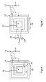
- Fig. 1 depicts a block diagram of a sample capacitive sensing array.
- Fig. 2 depicts a block diagram of an embodiment of a capacitive sensing array, as described herein.
- Fig. 3 depicts a sample electronic device incorporating the embodiment of a capacitive sensing array.
- Fig. 4 is a schematic illustration of a fingerprint sensing system according to an embodiment.
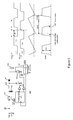
- Fig. 5 is a schematic illustration of an inductive boost circuit in accordance with an embodiment, together with a timing diagram showing example operation of the inductive boost circuit.
- Fig. 6 is a schematic illustration of another fingerprint sensing system in accordance with an embodiment.
- embodiments discussed herein may take the form of a capacitive sensor, such as a fingerprint sensor.
- the sensor may be formed from a capacitive sensing element array; each capacitive sensing element of the array may register a voltage that varies with the capacitance of a capacitive coupling.
- a finger may capacitively couple to the individual capacitive sensing elements of the sensor, such that the sensor may sense a capacitance between each capacitive sensing element and the flesh of the fingerprint.
- the capacitance signal may be detected by sensing the change in voltage on the capacitive sensing element as the relative voltage between the finger and the sensing chip is changed.
- the capacitance signal may be detected by sensing the change in charge received by the capacitive sensing elements as the relative voltage between the finger and the sensing chip is changed. Portions of the finger further away from the sensor may create a lower capacitance between the sensor and finger, and thus a lower signal on underlying capacitive sensing elements. By contrast, portions of the finger closer to the sensor may create a higher capacitance between sensor and finger, and thus higher signals on underlying capacitive sensing elements. Thus, capacitive sensing elements underlying ridges of a fingerprint may register higher signals while capacitive sensing elements underlying valleys of the fingerprint may register a lower capacitance and lower signals.
- the fingerprint sensor may include both a sensor pad and a drive ring. Both the sensor pad and drive ring may be placed beneath a dielectric, such that the finger does not directly touch either the sensor pad or drive ring but instead comes into contact with the interposed dielectric. In some examples, the finger may contact the drive ring.
- the difference in signals at the sensor capacitive sensing elements may be used to map a fingerprint.
- the resolution of the sensor may vary with capacitive sensing element density, distance between the sensor pad's surface and the finger, and thickness of a dielectric covering the sensor pad. Generally, as the dielectric increases in thickness, the capacitance between the finger and sensor grows increasingly attenuated, and so the signal differences may attenuate, as well. Certain embodiments may address this attenuation by applying a higher, less variable, relative voltage change between the finger and the sensor pad, leading to a higher detectable signal at the sensor, as described in more detail herein.
- the capacitive coupling between the sensor and finger may compensate for the thickness of the dielectric.
- the capacitance between finger and capacitive sensing elements of the sensor pad may be increased, thereby obtaining better resolution and imaging of the fingerprint.
- the sensor may be driven at a higher voltage, such as 12 volts peak-to-peak, 16 volts peak-to-peak, or even more, without inducing any physical sensation in the finger or hand of a user. This may be accomplished by maintaining the drive ring's voltage at a system ground voltage, while the sensor array is modulated with the higher peak-to-peak voltage signal.
- Fig. 2 depicts one sample embodiment of a fingerprint sensor.
- Sensor 200 may include sensor pad 202 formed by an array of individual capacitive sensing elements. Although sensor pad 202 is shown, the individual capacitive sensing elements are omitted for purposes of clarity.
- each capacitive sensing element may be capacitively coupled to a portion of finger 212 overlying that capacitive sensing element; the distance between the overlying finger portion and capacitive sensing element determines the capacitance between the two and thus the signal registered at the capacitive sensing element. As distance decreases, signal increases.
- Each capacitive sensing element is also capacitively coupled to other adjacent overlying finger portions, and as the distance increases, this leads to a blurring effect, which reduces the total signal difference between capacitive sensing elements directly under finger ridges and finger valleys.
- the fingerprint sensor may also include drive ring 204.
- Drive ring 204 may be maintained at a system ground voltage, rather than an absolute or earth ground.
- the fingerprint sensor may also include first and second drive amplifier 206 and 208, as depicted in Fig. 2 .
- First drive amplifier 206 may drive a sensor integrated circuit that includes sensor pad 202, such as an application-specific integrated circuit (ASIC) with a modulating voltage, to induce relative voltage between sensor pad 202 and user finger 212.
- Second drive amplifier 208 may, provide voltage and current to the sensor integrated circuit, so that the sensor integrated circuit can operate from the relative voltage difference between first and second drive amplifiers 206 and 208.
- Second drive amplifier 208 may supply a modulating voltage in sync with first drive amplifier 206, such that the relative voltage between the outputs of the first and second amplifiers is approximately constant.
- the first and second drive amplifiers may be connected by capacitor 210, which can help amplifiers 206 and 208 keep the relative voltage between the first and second drive amplifier outputs constant.
- Fig. 3 depicts electronic device 300 that may incorporate a fingerprint sensor, such as that shown in Fig. 2 .
- Electronic device 300 may be a mobile telephone, a tablet computing device, a notebook computer, a personal digital assistant, a desktop computer, a portable media player, and the like.
- the sensor pad may be placed below an input mechanism, such as button 302 of electronic device 300.
- the sensor pad may alternatively be placed beneath a portion of display screen 304 of electronic device 300, beneath sidewall 306 or other portion of the device's enclosure, and the like. Essentially, any portion of the electronic device's enclosure may house the fingerprint sensor.
- a fingerprint sensor chip (including both sensor pad and drive ring) may be positioned beneath the button 302.
- An ink layer and/or adhesive may be placed between the button's bottom surface and the sensor chip's top surface. The adhesive may bond the chip to the button, for example.
- One or more solder balls may affix the fingerprint sensor chip to a flex conductor. The solder balls may generally be placed near the center of the fingerprint sensor chip to reduce the likelihood of cracking due to stress.
- a number of fingerprint sensors as described herein may be employed in a single electronic device.
- the fingerprint sensors may be arranged beneath a cover glass or outer surface of an electronic device.
- the sensors may be arranged in an array or other ordered pattern.
- the sensors may be placed randomly or semi-randomly beneath the surface.
- the sensors may be placed within or beneath a display stack of an electronic device incorporating a display, such as a mobile phone, tablet computing device, computer display screen, and the like.
- the sensor(s) may capacitively sense a fingerprint through the display and/or cover glass of the display.
- a portion of the device enclosure or frame may serve as a ground ring as described herein.
- Multiple sensors may share a ground ring in such a configuration.
- the device may activate a fingerprint sensor at, under or near the location at which a touch was sensed.
- only fingerprint sensors corresponding to the touch location may be activated while others remain inactive.
- the ground ring e.g., portion of the housing, such as sidewall 306 may be coupled to the active fingerprint sensor to obtain a fingerprint or partial fingerprint and operate as generally described herein.
- one or more fingerprint sensors may be placed outside of the display area 304 but beneath a surface of the electronic device 300.
- one or more sensors may be located in a chin (e.g., a region below the display 304, such as the area around button 302) or a forehead (e.g., a region above the display 304) of the electronic device 300.
- flex circuit may extend from the input mechanism stack-up and connect the sensor chip to a signal provider chip that may facilitate modulating the voltage and/or operating frequency of the fingerprint sensor chip.
- the signal provider chip and fingerprint sensor chip may be provided as a single chip or distributed amongst a different number of chips. External components may also be used.
- an ASIC may be used as the signal provider chip. The ASIC may also communicate data to and from a processor of the electronic device.
- Fig. 4 is a schematic illustration of a fingerprint sensing system according to an embodiment.
- the fingerprint sensing system 400 includes a fingerprint sensor chip 405 and a signal provider chip 410.
- a drive ring 412 is also shown.
- the sensor provided by the fingerprint sensor chip may be modulated using a higher voltage, e.g. 16V peak-to-peak, while the drive ring 412 may be held at a system ground voltage.
- the system ground voltage may be provided by the signal provider chip 410 and is shown as NRING in Fig. 4 .
- the 16V peak-to-peak signal may be provided by the signal provider chip 410, and is shown as NGND in Fig. 4 .
- a sensor pad (not shown in Fig. 4 ) may be integrated into or coupled to the fingerprint sensor chip 405.
- the capacitive sensing element array may capacitively couple to a finger of a user's hand.
- the capacitive sensing element array may be modulated at a variety of frequencies.
- the capacitive sensing element array may measure the voltage of all capacitive sensing elements during a high voltage and again during a low voltage. That is, voltages supplied to the capacitive sensing element array and/or the sensor chip ground voltage, may generally resemble a square wave, although in alternative embodiments the voltage may take other wave shapes.
- a modulator (labeled "mod. block” in Fig. 4 ) may control the modulation or oscillation of the capacitive sensing element array and/or the sensor chip ground voltage in accordance with a clock signal, NDRV in Fig. 4 .
- the difference between the capacitive sensing element voltages and/or charges, as measured during the high and low portions of the modulation cycle, permits the chip to determine the capacitance between each capacitive sensing element and overlying portion of the finger and thus the capacitance. From the capacitance with each capacitive sensing element, the fingerprint may be sensed, measured and reconstructed as known to those skilled in the art and generally discussed above.
- the signal provider chip 410 may provide a modulated high voltage signal (e.g. 16V peak-to-peak) to the fingerprint sensor chip 405 for use in modulating the sensor. While 16V is used here as an example, in other examples different voltages may be used, including voltages greater than 4V in some examples, greater than 6V in some examples, greater than 8V in some examples, greater than 10V in some examples, greater than 12V in some examples, greater than 14V in some examples, and greater than 16V in some examples.
- the signal provider chip 410 may further provide a ground voltage, shown as NRING in Fig. 4 to the drive ring 412. Other voltages for NRING may be used in other examples, including 4V, less than 4V, less than 2V, or negative voltages.
- the drive ring 412 may be kept at a voltage that may not be felt by a user touching the drive ring 412 but that has a sufficient difference in magnitude from the voltage provided to the sensor (e.g. NGND) to provide suitable signal-to-noise ratio for fingerprint sensing. In one example, that difference in magnitude is 16V, with the sensor voltage provided being 16V and the drive ring held at a ground voltage.
- Example components of the fingerprint sensing system 400 used to form an inductive boost circuit to provide the NGND signal (which may be, e.g. 16V) will now be described. Reference will be made to transistors 421, 422, and 423, inductor 425, timing block 427, diode 442, diode 443, and level translators 430.
- a clock signal e.g. NDRV of Fig. 4
- the clock signal may be provided to a level translator 430 prior to receipt by the timing block 427 in some examples.
- the level translator 430 may function to change a magnitude of the clock signal in some examples where, e.g. the timing block may operate in a different supply power domain than the fingerprint sensor chip 405.
- the timing block 425 may output respective versions of the clock signal (e.g. NDRV) to the gates of the transistors 421, 422, and 423.
- the respective versions of the clock signals may be delayed varying amounts as applied by the timing block 427.
- the timing block may include one or more delay circuits configured to delay the clock signal (e.g. NDRV) prior to providing a delayed signal to the transistors 421, 422, and/or 423.
- the transistor 423 may serve as a pass transistor.
- the transistor 423 may turn on when a clock signal, e.g. NDRV, is provided to the timing block 427.
- a clock signal e.g. NDRV
- the signal provided by the timing block to a gate of the transistor 423 may be indicative of the presence or absence of a clock signal (e.g. NDRV).
- the transistor 423 may be turned on when the fingerprint sensor chip 405 is active and may be turned off when the fingerprint sensor chip 405 is inactive.
- the signal provided by the timing block 427 to the gate of the transistor 423 may be provided through an optional gate driver circuit as shown.
- a supply voltage e.g.
- 1.8 V in some examples may be provided to the inductor 425, to allow the inductor 425 to store energy.
- the inductor may charge capacitor 432 to a boosted voltage, e.g. a voltage greater than the power supply voltage. In some examples, the inductor provides a boosted voltage of 16 V.
- capacitor 432 can be implemented as a physical component of the system, in some embodiments the capacitor 432 may be implemented as the parasitic capacitance of the fingerprint sensor 405 to the environment and the system ground, and combinations of these may be used in some embodiments.
- the transistor 421 may function to chop a voltage provided by the inductor 425 at a frequency expected by the fingerprint sensor chip 405, such as 2 MHz in some examples. In some examples, the transistor 421 may chop the voltage at a same frequency as the clock signal, e.g. NDRV. When the transistor 421 is off, the voltage NGND may be a boosted power supply voltage developed by the inductor 425, e.g. 16V. When the transistor 421 is on, the current flowing in the inductor 425 may find a path to ground, and the voltage NGND may transition to ground. Accordingly, the transistor 421 may be switched at a particular frequency to achieve a shaped 16V peak-to-peak waveform. Other peak voltages may also be used.
- the switched frequency is the same as the frequency of the clock signal, e.g. NDRV.
- the timing block 427 may delay the clock signal, e.g. NDRV, a particular amount and provide a delayed clock signal (e.g. delayed NDRV) to a gate of the transistor 421.
- the amount of delay may be related to the desired NGND voltage. In one example, the delay is 25 ns when a 2 MHz clock is used.
- the NGND signal provided at the node labeled NGND may be a boosted (e.g. 16 V) square wave signal at a frequency of 2 MHz. Other frequencies and voltages may be used.
- the inductor 425 may then be coupled to parasitic capacitances, shown in Fig. 4 as C para 432.
- the parasitic capacitances may represent, for example, capacitance between the fingerprint sensor chip 405 and ground, and may include capacitances through a body of the user touching the fingerprint sensor.
- oscillation of the boosted voltage (e.g. NGND) signal may occur.
- the transistor 422 may be provided.
- the transistor 422 When turned on, the transistor 422 may advantageously divert the current from the inductor 423 to damp oscillations which otherwise may occur. Accordingly, the timing block 427 may provide a version, which may be a delayed version, of the clock signal (e.g. NDRV) to the gate of the transistor 422.
- the clock signal (e.g. NDRV) may be delayed by the timing block 427 an amount sufficient such that when the transistor 422 turns on, the voltage NGND has already reached the target voltage (e.g. 16V).
- an inductive boost circuit may be used to provide a boosted voltage (e.g. 16 V) at the node labeled NGND in Fig. 4 (after the diode 443).
- the boosted voltage may be provided to the fingerprint sensor chip 405 for use in modulating the sensor.
- the boosted voltage itself may be provided as a modulated signal having a frequency, which may be the same as a frequency of the system clock signal (e.g. NDRV).
- the low dropout regulator (LDO) 450 may provide a constant supply voltage to the fingerprint sensor chip (e.g. 1.8V). This voltage is provided respectively to the node NGND which can be at the system ground voltage or the boosted voltage.
- the four communication lines labeled SCLK, MOSI, MISO and INT generally permit data to be transferred to and from the fingerprint sensor chip.
- the signals may be provided through the level translator 430.
- the communication lines are referenced to the sensor ground NGND that is different from the system ground.
- the level translator may allow for communication to happen between the NGND referenced fingerprint sensor chip and the system ground (GND) referenced device processor.
- the communication may happen synchronously or asynchronously with the modulation signal NDRV.
- the node NGND can be at the system ground voltage or at the boosted voltage.
- SCLK is the serial communication clock and may be used for timing operations.
- the MISO line may be used for master/slave transmission of data from a slave to a master.
- the fingerprint sensor chip may be the slave, while a processor associated with the electronic device incorporating the sensor may be the master.
- the MOSI line may be used for sending data from the master (e.g., device processor) to the slave (e.g., fingerprint sensor chip).
- the INT line may be used for interrupts.
- the fingerprint sensor chip may use the INT line to provide a signal indicating to the device processor that the fingerprint sensor chip has completed a task or that the fingerprint sensor chip has some fingerprint data ready to be transferred.
- the fingerprint sensor chip 405 may operate in a relatively low-power state.
- the chip may initiate a scanning operation.
- the chip may detect a nearby finger by measuring a capacitance change of one or more capacitive sensing elements of the array relative to its ground, as one example. This may cause the chip to begin a scanning operation.
- the scanning operation generally may include reading the voltage or charge of one or more of the capacitive sensing elements during a low-voltage state of the array or sensor chip ground, driving the array or sensor chip ground to a high voltage and again reading the voltage or charge of one or more of the capacitive sensing elements.
- the scanning operation may alternately include reading the voltage or charge of one or more of the capacitive sensing elements during a high-voltage state of the array or sensor chip ground, driving the capacitive sensing element array or sensor chip ground to a low voltage and again reading the voltage or charge of one or more of the capacitive sensing elements.
- the capacitive sensing elements may be modulated at a relatively high frequency between the low and high voltage states by the modulator.
- the chip may operate at a two megahertz frequency, although other embodiments may employ higher or lower frequencies.
- the drive ring may not be modulated with the capacitive sensing element array. Rather, the drive ring's potential may remain constant at system ground or very near to system ground. This may help prevent or reduce excitation and/or modulation of the finger, which in turn permits the use of higher voltages to drive the capacitive sensing element array.
- the fingerprint sensor is incorporated into a handheld device such as the mobile device of Fig. 3
- other fingers of the user's hand may be in contact with a metal portion, or other conductive portion, of the enclosure.
- the enclosure generally is also at system ground, so contact between conductive elements on the enclosure and the user's hand facilitate driving or maintaining the voltage of the sensed finger to system ground.
- the "sensed finger” is the finger overlaying the sensor pad, or the finger being imaged by the fingerprint sensor. Maintaining the sensed finger at or near system ground may enhance resolution of the fingerprint image and assist in preventing modulation of the finger.
- Fig. 5 is a schematic illustration of an inductive boost circuit in accordance with an embodiment, together with a timing diagram showing example operation of the inductive boost circuit.
- the inductive boost circuit 500 is the same used in the fingerprint sensing system 400 of Fig. 4 , and like components are labeled with like reference numbers, the details of which are not repeated here for brevity. Operation of the inductive boost circuit 500 will be described with reference to the timing diagram shown in Fig. 5 for added clarity.
- the transistor 423 may function as a pass transistor that may be on whenever an active clock signal (e.g. NDRV) is present. Accordingly, for the purposes of discussion of Fig. 5 , the transistor 423 is assumed ON during operations described with reference to Fig. 5 .
- the diode 442 may be used only when transistor 423 turns off following a fingerprint scan. Accordingly, the diode 442 is assumed OFF during described operations with reference to Fig. 5 .
- the transistor 421 may turn off (e.g. the gate voltage shown in the trace related to transistor 421 of Fig. 5 may transition low, turning the transistor 421 off).
- the inductor current I L decreases as the voltage at node NGND begins to rise to the boosted voltage (e.g. 16V) as shown in the timing diagram traces labeled I L and NGND.
- the voltage of NGND may peak at time t 1 , as shown, where t 1 may represent an inductor voltage buildup time following to.
- the diode 443 may turn off, not allowing current to flow through the diode 443 to capacitor 432, and thus maintaining the voltage on NGND.
- the transistor 422 may turn on (e.g. the gate voltage shown in the trace related to transistor 422 of Fig. 5 may transition high, turning the transistor 422 on). This may allow damping through the transistor 422 to prevent or reduce oscillations in NGND.
- the transistor 421 may be turned on (e.g. the gate voltage shown in the trance related to transistor 421 of Fig. 5 may transition high, turning the transistor 421 on). When the transistor 421 is turned on, the voltage NGND may be returned to ground as the capacitor 432 is discharged through the transistor 421. Accordingly, the NGND signal falls back to ground starting at time t 3 .
- the transistor 422 is turned off (e.g. the gate voltage shown in the trace related to transistor 422 of Fig. 5 may transition low, turning the transistor 422 off).
- the diode 443 may accordingly turn on, allowing current to flow, but since the transistor 421 remains on, the current may not charge the node NGND until the transistor 421 is again turned off.
- Fig. 6 is a schematic illustration of another fingerprint sensing system in accordance with an embodiment.
- the fingerprint sensing system 600 includes a fingerprint sensor chip 605, and a signal provider chip 610, which may be implemented using the fingerprint sensor chip 405 and signal provider chip 410 of Fig. 4 , respectively.
- Drive ring 612 and fingerprint receiving surface 614 are also shown.
- External components inductor 625 and diodes 642 and 643 are shown which may be used by the signal provider chip 610 in providing a boosted voltage (e.g. NGND) during fingerprint scans.
- the inductor 625 and diodes 642 and 643 may be implemented using the inductor 425 and diodes 442 and 443 of Fig.
- the signal provider chip may include remaining components of the inductive boost circuit 500 of Fig. 5 , for example.
- GND-referenced domain 650 two domains are shown GND-referenced domain 650 and NGND-referenced domain 652.
- operations may occur using a system ground (GND).
- NGND-referenced domain operations may occur using a boosted ground (NGND).
- the boosted ground signal (e.g. NGND) may only be boosted at particular times, such as during a scan.
- the boosted ground signal (e.g. NGND) may be modulated such that it has a frequency, which frequency may equal a frequency of a clock signal used by the system (e.g. NDRV).
- the fingerprint receiving surface 614 may be made of an insulating material preventing the finger from being in contact with the sensor chip 605 and affected by the boosted voltage. Accordingly inputs to the fingerprint sensor chip 605 may be referenced against NGND, and not system ground.
Landscapes
- Engineering & Computer Science (AREA)
- Theoretical Computer Science (AREA)
- Human Computer Interaction (AREA)
- Physics & Mathematics (AREA)
- General Physics & Mathematics (AREA)
- Multimedia (AREA)
- General Engineering & Computer Science (AREA)
- Measurement Of Length, Angles, Or The Like Using Electric Or Magnetic Means (AREA)
- Image Input (AREA)
- Measurement Of The Respiration, Hearing Ability, Form, And Blood Characteristics Of Living Organisms (AREA)
Applications Claiming Priority (5)
| Application Number | Priority Date | Filing Date | Title |
|---|---|---|---|
| US201261623941P | 2012-04-13 | 2012-04-13 | |
| US201261649203P | 2012-05-18 | 2012-05-18 | |
| US201261666579P | 2012-06-29 | 2012-06-29 | |
| US201261666610P | 2012-06-29 | 2012-06-29 | |
| US13/842,635 US9740343B2 (en) | 2012-04-13 | 2013-03-15 | Capacitive sensing array modulation |
Publications (2)
| Publication Number | Publication Date |
|---|---|
| EP2650823A2 true EP2650823A2 (de) | 2013-10-16 |
| EP2650823A3 EP2650823A3 (de) | 2014-01-22 |
Family
ID=48128144
Family Applications (1)
| Application Number | Title | Priority Date | Filing Date |
|---|---|---|---|
| EP13163827.2A Ceased EP2650823A3 (de) | 2012-04-13 | 2013-04-15 | Kapazitive Abtastarraymodulierung |
Country Status (7)
| Country | Link |
|---|---|
| US (2) | US9740343B2 (de) |
| EP (1) | EP2650823A3 (de) |
| CN (3) | CN103376970B (de) |
| AU (3) | AU2013204080B2 (de) |
| NL (1) | NL2010604C2 (de) |
| TW (2) | TWI536275B (de) |
| WO (1) | WO2013154885A2 (de) |
Cited By (13)
| Publication number | Priority date | Publication date | Assignee | Title |
|---|---|---|---|---|
| WO2015005855A1 (en) * | 2013-07-09 | 2015-01-15 | Fingerprint Cards Ab | Fingerprint sensing system and method |
| WO2015183170A1 (en) * | 2014-05-28 | 2015-12-03 | Fingerprint Cards Ab | Electronic device with fingerprint sensing system and conducting housing |
| WO2016043643A1 (en) * | 2014-09-15 | 2016-03-24 | Fingerprint Cards Ab | Fingerprint sensor with sync signal input |
| EP3016026A3 (de) * | 2014-10-31 | 2016-05-11 | eMemory Technology Inc. | Integriertes Kapazitätserfassungsmodul und zugehöriges System |
| WO2016130070A1 (en) * | 2015-02-11 | 2016-08-18 | Fingerprint Cards Ab | Capacitive fingerprint sensing device with current readout from sensing elements |
| EP3109793A1 (de) * | 2015-06-22 | 2016-12-28 | Nxp B.V. | System zum erkennen von fingerabdrücken |
| US9710690B1 (en) | 2016-04-22 | 2017-07-18 | Fingerprint Cards Ab | Fingerprint sensing system with adaptive power control |
| US9864895B1 (en) | 2016-07-07 | 2018-01-09 | Fingerprint Cards Ab | Fingerprint sensing system with finger detect |
| EP3308324A4 (de) * | 2015-06-10 | 2018-07-18 | BYD Company Limited | Verfahren und vorrichtung zur anpassung der erregungsspannung eines fingerabdruckerkennungschips |
| EP3242246A4 (de) * | 2014-12-30 | 2018-08-01 | Shenzhen Goodix Technology Co., Ltd. | Fingerabdruckerkennungssensor und endgerätevorrichtung |
| EP3418942A4 (de) * | 2016-11-21 | 2019-05-15 | Shenzhen Goodix Technology Co., Ltd. | Fingerabdrucksensor und elektronisches endgerät |
| EP3385881A4 (de) * | 2015-12-02 | 2019-07-10 | Microarray Microelectronics Corp., Ltd | Kapazitiver fingerabdrucksensor |
| TWI679431B (zh) * | 2018-07-31 | 2019-12-11 | 友達光電股份有限公司 | 指紋感測裝置及其檢測方法 |
Families Citing this family (72)
| Publication number | Priority date | Publication date | Assignee | Title |
|---|---|---|---|---|
| US8416198B2 (en) * | 2007-12-03 | 2013-04-09 | Apple Inc. | Multi-dimensional scroll wheel |
| US9740343B2 (en) | 2012-04-13 | 2017-08-22 | Apple Inc. | Capacitive sensing array modulation |
| US9030440B2 (en) | 2012-05-18 | 2015-05-12 | Apple Inc. | Capacitive sensor packaging |
| US9994179B2 (en) * | 2012-07-25 | 2018-06-12 | Infineon Technologies Austria Ag | Circuit arrangements and a method for receiving information |
| US9883822B2 (en) | 2013-06-05 | 2018-02-06 | Apple Inc. | Biometric sensor chip having distributed sensor and control circuitry |
| NL2012891B1 (en) | 2013-06-05 | 2016-06-21 | Apple Inc | Biometric sensor chip having distributed sensor and control circuitry. |
| KR101368262B1 (ko) * | 2013-06-10 | 2014-02-28 | (주)드림텍 | 외관부재 접합방식 지문인식 홈키 제조방법 |
| KR101368804B1 (ko) * | 2013-06-26 | 2014-03-03 | (주)드림텍 | 데코 부품의 단차 구조가 적용된 지문인식 홈키 제조방법 및 그 지문인식 홈키 구조 |
| US9984270B2 (en) | 2013-08-05 | 2018-05-29 | Apple Inc. | Fingerprint sensor in an electronic device |
| JP6654566B2 (ja) * | 2013-08-23 | 2020-02-26 | フィンガープリント カーズ アーベー | 指紋検知システムの接続パッド |
| US10296773B2 (en) | 2013-09-09 | 2019-05-21 | Apple Inc. | Capacitive sensing array having electrical isolation |
| US9460332B1 (en) | 2013-09-09 | 2016-10-04 | Apple Inc. | Capacitive fingerprint sensor including an electrostatic lens |
| US9697409B2 (en) | 2013-09-10 | 2017-07-04 | Apple Inc. | Biometric sensor stack structure |
| KR102256677B1 (ko) | 2013-12-02 | 2021-05-28 | 삼성디스플레이 주식회사 | 플렉서블 표시장치 및 이의 영상 표시방법 |
| PL3087349T3 (pl) | 2013-12-27 | 2025-10-20 | Byd Semiconductor Company Limited | Pojemnościowe urządzenie wykrywające do identyfikacji odcisków palców oraz urządzenie do identyfikacji odcisków palców zawierające wspomniane urządzenie |
| WO2015101266A1 (en) | 2013-12-30 | 2015-07-09 | Byd Company Limited | Sensor for detecting fingerprint and fingerprint identification apparatus and controlling method of sensor for detecting fingerprint |
| JP6212648B2 (ja) | 2014-01-14 | 2017-10-11 | フォーカルテック エレクトロニクス リミテッドFocaltech Electronics, Ltd. | 電界型指紋認証装置及びその状態制御方法、プロテーゼ認証方法 |
| US9152841B1 (en) * | 2014-03-24 | 2015-10-06 | Fingerprint Cards Ab | Capacitive fingerprint sensor with improved sensing element |
| US9582127B2 (en) | 2014-04-04 | 2017-02-28 | Synaptics Incorporated | Large feature biometrics using capacitive touchscreens |
| CN105094293A (zh) * | 2014-05-09 | 2015-11-25 | 敦泰电子有限公司 | 一种电子设备 |
| CN104036263A (zh) * | 2014-07-02 | 2014-09-10 | 南昌欧菲生物识别技术有限公司 | 指纹识别检测装置、终端设备及指纹识别方法 |
| CN104182745B (zh) * | 2014-08-15 | 2017-09-22 | 深圳市汇顶科技股份有限公司 | 指纹感应信号的处理方法、系统及指纹识别终端 |
| CN104298962B (zh) * | 2014-09-04 | 2018-04-27 | 深圳市汇顶科技股份有限公司 | 指纹检测装置和方法 |
| CN105512601B (zh) * | 2014-09-29 | 2019-12-27 | 神盾股份有限公司 | 指纹感测装置及其感测方法 |
| US9628594B2 (en) * | 2014-10-31 | 2017-04-18 | Semtech Corporation | Method and device for capacitive near-field communication in mobile devices |
| CN104318222B (zh) * | 2014-11-14 | 2019-10-11 | 深圳市汇顶科技股份有限公司 | 用于指纹检测的检测方法和装置 |
| US9449212B2 (en) * | 2014-12-22 | 2016-09-20 | Fingerprint Cards Ab | Capacitive fingerprint sensor with sensing elements comprising timing circuitry |
| CN104538385A (zh) * | 2015-01-13 | 2015-04-22 | 深圳市亚耕电子科技有限公司 | 多芯片封装结构以及电子设备 |
| CN105793869A (zh) * | 2015-01-13 | 2016-07-20 | 深圳信炜科技有限公司 | 电子设备及其电容式感测系统、以及电容式感测系统的检测方法 |
| CN104516716A (zh) * | 2015-01-13 | 2015-04-15 | 深圳市亚耕电子科技有限公司 | 电子设备及其电容式感测系统、以及电容式感测系统的检测方法 |
| CN105893918A (zh) * | 2015-01-26 | 2016-08-24 | 胡家安 | 一种指纹检测装置及方法 |
| TWI560617B (en) * | 2015-02-13 | 2016-12-01 | Byd Co Ltd | Fingerprint detection circuit and electronic device |
| US9817506B2 (en) | 2015-03-31 | 2017-11-14 | Synaptics Incorporated | Sensor array configurations for differential readout |
| US9740326B2 (en) | 2015-03-31 | 2017-08-22 | Synaptics Incorporated | Sensor array with split-drive differential sensing |
| US9823794B2 (en) | 2015-03-31 | 2017-11-21 | Synaptics Incorporated | Differential readout for sensor array |
| CN105448858B (zh) * | 2015-06-10 | 2018-03-13 | 比亚迪股份有限公司 | 指纹检测芯片的封装测试装置和方法 |
| US10095948B2 (en) * | 2015-06-30 | 2018-10-09 | Synaptics Incorporated | Modulation scheme for fingerprint sensing |
| TWI547884B (zh) * | 2015-07-09 | 2016-09-01 | 金佶科技股份有限公司 | 指紋辨識模組 |
| CN106971149A (zh) * | 2015-07-24 | 2017-07-21 | 深圳市汇顶科技股份有限公司 | 指纹检测电路及指纹辨识系统 |
| CN105095874B (zh) * | 2015-07-31 | 2018-10-16 | 京东方科技集团股份有限公司 | 指纹识别电路、驱动控制电路、显示基板和显示装置 |
| KR102334381B1 (ko) | 2015-08-10 | 2021-12-02 | 삼성전자 주식회사 | 그라운드 모듈레이션을 이용하는 터치 디스플레이 시스템 |
| CN105094494B (zh) | 2015-09-15 | 2019-08-23 | 京东方科技集团股份有限公司 | 指纹识别方法、装置及电子设备 |
| CN105138205A (zh) * | 2015-09-23 | 2015-12-09 | 深圳信炜科技有限公司 | 电容式传感器、传感装置、感测系统、以及电子设备 |
| KR20170039025A (ko) * | 2015-09-30 | 2017-04-10 | 삼성디스플레이 주식회사 | 표시 장치 |
| US10282585B2 (en) | 2015-11-13 | 2019-05-07 | Cypress Semiconductor Corporation | Sensor-compatible overlay |
| US9639734B1 (en) | 2015-11-13 | 2017-05-02 | Cypress Semiconductor Corporation | Fingerprint sensor-compatible overlay material |
| US10832029B2 (en) | 2015-11-13 | 2020-11-10 | Cypress Semiconductor Corporation | Sensor-compatible overlay |
| US9600707B1 (en) * | 2015-11-30 | 2017-03-21 | Fingerprint Cards Ab | Analog sampling system and method for noise supression |
| EP3217316A1 (de) * | 2016-03-11 | 2017-09-13 | Nxp B.V. | Fingerabdruckerfassungssystem und -verfahren |
| US9773153B1 (en) * | 2016-03-24 | 2017-09-26 | Fingerprint Cards Ab | Fingerprint sensor module |
| CN106022270B (zh) * | 2016-03-31 | 2019-08-20 | 深圳市奔凯安全技术股份有限公司 | 一种指纹检测电路及装置 |
| WO2017185247A1 (zh) * | 2016-04-27 | 2017-11-02 | 深圳市汇顶科技股份有限公司 | 芯片测试方法及装置 |
| KR20180014682A (ko) * | 2016-06-13 | 2018-02-09 | 선전 구딕스 테크놀로지 컴퍼니, 리미티드 | 터치 검출 회로, 지문 모듈 및 그 제어 방법 |
| EP3264242A1 (de) * | 2016-06-29 | 2018-01-03 | Saint-Gobain Glass France | Berührungssteuerungsverglasungen mit kapazitiver berührungsempfindlicher vorrichtung und einer lichtemittierenden diode und herstellung davon |
| TWI730111B (zh) * | 2016-07-25 | 2021-06-11 | 瑞典商指紋卡公司 | 用於確定手指移動事件的方法和指紋感測系統 |
| TWI602100B (zh) * | 2016-07-29 | 2017-10-11 | 義隆電子股份有限公司 | 指紋感測裝置的操作方法及指紋感測系統 |
| CN106469303B (zh) * | 2016-09-18 | 2019-07-09 | 京东方科技集团股份有限公司 | 指纹光电流检测单元、指纹识别器、驱动方法和显示装置 |
| EP3324331B1 (de) * | 2016-09-27 | 2020-11-25 | Shenzhen Goodix Technology Co., Ltd. | Kapazitive messschaltung |
| WO2018076283A1 (zh) * | 2016-10-28 | 2018-05-03 | 敦泰电子有限公司 | 一种指纹感测芯片及终端设备 |
| US10102412B2 (en) * | 2016-11-17 | 2018-10-16 | Fingerprint Cards Ab | Fingerprint sensing with different capacitive configurations |
| CN106529509B (zh) * | 2016-12-08 | 2019-11-22 | 江苏邦融微电子有限公司 | 一种指纹传感器采集像素单元电路 |
| CN106599822B (zh) * | 2016-12-08 | 2019-11-12 | 江苏邦融微电子有限公司 | 一种可变分辨率的指纹采集单元阵列及其采集方法 |
| US10540044B2 (en) | 2016-12-14 | 2020-01-21 | Cypress Semiconductor Corporation | Capacitive sensing with multi-pattern scan |
| KR102090508B1 (ko) * | 2016-12-29 | 2020-03-19 | 선전 구딕스 테크놀로지 컴퍼니, 리미티드 | 터치 시스템 및 그 전원 회로 |
| WO2018138651A1 (en) * | 2017-01-24 | 2018-08-02 | Idex Asa | Configurable, encapsulated sensor module and method for making same |
| KR102534186B1 (ko) | 2017-11-10 | 2023-05-19 | 삼성전자주식회사 | 지문 센서를 포함하는 전자 장치 |
| WO2019131001A1 (ja) * | 2017-12-28 | 2019-07-04 | コネクテックジャパン株式会社 | 画像取得装置およびそれを備える表示装置 |
| US10650214B2 (en) * | 2018-04-24 | 2020-05-12 | Image Match Design Inc. | Fingerprint sensor and method of fingerprint detection |
| KR102596042B1 (ko) * | 2018-06-27 | 2023-10-31 | 엘지디스플레이 주식회사 | 지문 인식형 표시장치 |
| CN110531896B (zh) * | 2019-08-29 | 2024-03-29 | 珠海市宏沛函电子技术有限公司 | 一种触控驱动方法、触控驱动装置及触控面板 |
| TWI706625B (zh) * | 2020-04-09 | 2020-10-01 | 義隆電子股份有限公司 | 感應式電子辨識裝置及其供電補償電路 |
| CN111714091A (zh) * | 2020-06-30 | 2020-09-29 | 京东方科技集团股份有限公司 | 一种皮肤状况检测装置、方法和远程医疗系统 |
Citations (4)
| Publication number | Priority date | Publication date | Assignee | Title |
|---|---|---|---|---|
| US5650597A (en) | 1995-01-20 | 1997-07-22 | Dynapro Systems, Inc. | Capacitive touch sensor |
| US6628812B1 (en) | 1999-05-11 | 2003-09-30 | Authentec, Inc. | Fingerprint sensor package having enhanced electrostatic discharge protection and associated methods |
| US6734655B1 (en) | 2000-06-30 | 2004-05-11 | Intel Corporation | Regulator design for inductive booster pump using pulse width modulation technique |
| US20120085822A1 (en) | 2010-10-08 | 2012-04-12 | Authentec, Inc. | Finger sensing device including differential measurement circuitry and related methods |
Family Cites Families (187)
| Publication number | Priority date | Publication date | Assignee | Title |
|---|---|---|---|---|
| US3876942A (en) | 1973-09-21 | 1975-04-08 | Aero Electronics Dev Co Inc | Emergency airplane locating transmitter |
| US4221418A (en) | 1977-11-24 | 1980-09-09 | Ateliers J. Hanrez S.A. | Apparatus for handling a cover of a steam generator in an electro-nuclear station |
| US4421418A (en) | 1981-04-02 | 1983-12-20 | Rhythm Watch Co., Ltd. | Clock adjustment switch system |
| GB2244164A (en) | 1990-05-18 | 1991-11-20 | Philips Electronic Associated | Fingerprint sensing |
| JP3138518B2 (ja) | 1992-01-27 | 2001-02-26 | 多摩川精機株式会社 | ジャイロ装置 |
| US5731222A (en) | 1995-08-01 | 1998-03-24 | Hughes Aircraft Company | Externally connected thin electronic circuit having recessed bonding pads |
| US6049620A (en) | 1995-12-15 | 2000-04-11 | Veridicom, Inc. | Capacitive fingerprint sensor with adjustable gain |
| JP4024335B2 (ja) * | 1996-01-26 | 2007-12-19 | ハリス コーポレイション | 集積回路のダイを露出させる開口部を有する集積回路装置とその製造方法 |
| US6067368A (en) | 1996-01-26 | 2000-05-23 | Authentec, Inc. | Fingerprint sensor having filtering and power conserving features and related methods |
| CN1164076A (zh) | 1996-01-26 | 1997-11-05 | 哈里公司 | 安全性高的指纹感测盒及有关方法 |
| US5963679A (en) | 1996-01-26 | 1999-10-05 | Harris Corporation | Electric field fingerprint sensor apparatus and related methods |
| FR2749955B1 (fr) | 1996-06-14 | 1998-09-11 | Thomson Csf | Systeme de lecture d'empreintes digitales |
| US6088471A (en) | 1997-05-16 | 2000-07-11 | Authentec, Inc. | Fingerprint sensor including an anisotropic dielectric coating and associated methods |
| US6259804B1 (en) * | 1997-05-16 | 2001-07-10 | Authentic, Inc. | Fingerprint sensor with gain control features and associated methods |
| US5953441A (en) | 1997-05-16 | 1999-09-14 | Harris Corporation | Fingerprint sensor having spoof reduction features and related methods |
| US6011859A (en) | 1997-07-02 | 2000-01-04 | Stmicroelectronics, Inc. | Solid state fingerprint sensor packaging apparatus and method |
| US6483931B2 (en) | 1997-09-11 | 2002-11-19 | Stmicroelectronics, Inc. | Electrostatic discharge protection of a capacitve type fingerprint sensing array |
| GB9725571D0 (en) | 1997-12-04 | 1998-02-04 | Philips Electronics Nv | Electronic apparatus comprising fingerprint sensing devices |
| US6041410A (en) | 1997-12-22 | 2000-03-21 | Trw Inc. | Personal identification fob |
| EP0941696A1 (de) | 1998-03-03 | 1999-09-15 | Siemens Aktiengesellschaft | Fingertippsensor mit integriertem Tastschalter |
| JP2000076014A (ja) | 1998-08-27 | 2000-03-14 | Pentel Kk | 静電容量式タッチパネル装置 |
| AU2147900A (en) | 1998-11-12 | 2000-05-29 | Broadcom Corporation | Fully integrated tuner architecture |
| JP2000172833A (ja) | 1998-12-10 | 2000-06-23 | Omron Corp | 指紋照合装置 |
| JP3678927B2 (ja) | 1998-12-24 | 2005-08-03 | 株式会社リコー | 複写装置 |
| US6346739B1 (en) * | 1998-12-30 | 2002-02-12 | Stmicroelectronics, Inc. | Static charge dissipation pads for sensors |
| AU1573901A (en) | 1999-10-21 | 2001-04-30 | George Vlasios Kontos | Integrated security system with fingerprint imaging doorbell |
| KR100325381B1 (ko) | 2000-02-11 | 2002-03-06 | 안준영 | 지문입력기를 이용한 터치패드 구현방법 및지문입력기능을 하는 터치패드 장치 |
| DE50011685D1 (de) | 2000-04-14 | 2005-12-29 | Infineon Technologies Ag | Kapazitiver biometrischer Sensor |
| JP3713418B2 (ja) | 2000-05-30 | 2005-11-09 | 光正 小柳 | 3次元画像処理装置の製造方法 |
| JP2001344605A (ja) | 2000-05-31 | 2001-12-14 | Ricoh Co Ltd | 個人認証方法、その装置及びそのシステム |
| US20020065054A1 (en) | 2000-11-29 | 2002-05-30 | Morris Humphreys | Mobile station and elastomeric cover |
| US6914517B2 (en) | 2001-04-17 | 2005-07-05 | Dalton Patrick Enterprises, Inc. | Fingerprint sensor with feature authentication |
| CA2419678C (en) * | 2001-06-26 | 2008-04-01 | Casio Computer Co., Ltd. | Image acquisition apparatus |
| US7043060B2 (en) | 2001-07-17 | 2006-05-09 | Niccole Family Trust | Fingerprint-actuated padlock |
| US6672174B2 (en) | 2001-07-23 | 2004-01-06 | Fidelica Microsystems, Inc. | Fingerprint image capture device with a passive sensor array |
| JP2003298753A (ja) | 2002-03-29 | 2003-10-17 | Digital Electronics Corp | インターフォン装置 |
| EP2560199B1 (de) | 2002-04-05 | 2016-08-03 | STMicroelectronics S.r.l. | Verfahren zum Herstellen einer durchisolierten Verbindung in einem Körper aus einem Halbleitermaterial |
| CN1212588C (zh) | 2002-04-10 | 2005-07-27 | 祥群科技股份有限公司 | 电容式指纹读取芯片 |
| US6882338B2 (en) | 2002-08-16 | 2005-04-19 | Leapfrog Enterprises, Inc. | Electrographic position location apparatus |
| FI20030102A0 (fi) | 2003-01-22 | 2003-01-22 | Nokia Corp | Henkilön varmennusjärjestely |
| WO2004077340A1 (en) | 2003-02-28 | 2004-09-10 | Idex Asa | Substrate multiplexing with active switches |
| US6996492B1 (en) | 2003-03-18 | 2006-02-07 | Kla-Tencor Technologies Corporation | Spectrum simulation for semiconductor feature inspection |
| JP4160851B2 (ja) * | 2003-03-31 | 2008-10-08 | 富士通株式会社 | 指紋認識用半導体装置 |
| US7627151B2 (en) | 2003-04-04 | 2009-12-01 | Lumidigm, Inc. | Systems and methods for improved biometric feature definition |
| JP2004310574A (ja) | 2003-04-09 | 2004-11-04 | Matsushita Electric Ind Co Ltd | 凹凸パターン検出装置、その製造方法および携帯機器 |
| WO2004093005A1 (ja) | 2003-04-15 | 2004-10-28 | Fujitsu Limited | 情報処理装置 |
| JP3775601B2 (ja) | 2003-04-17 | 2006-05-17 | セイコーエプソン株式会社 | 静電容量検出装置及びその駆動方法、指紋センサ並びにバイオメトリクス認証装置 |
| KR20030043840A (ko) | 2003-04-25 | 2003-06-02 | (주)실리콘이미지웍스 | 지문인식센서를 구비한 휴대 통신단말기 |
| US6906529B2 (en) | 2003-06-10 | 2005-06-14 | Stmicroelectronics, Inc. | Capacitive sensor device with electrically configurable pixels |
| JP2005011672A (ja) | 2003-06-19 | 2005-01-13 | Omron Corp | 押しボタンスイッチ |
| US7202764B2 (en) | 2003-07-08 | 2007-04-10 | International Business Machines Corporation | Noble metal contacts for micro-electromechanical switches |
| US7236765B2 (en) | 2003-07-24 | 2007-06-26 | Hunt Technologies, Inc. | Data communication over power lines |
| JP4157557B2 (ja) | 2003-08-15 | 2008-10-01 | 日本電信電話株式会社 | 生体認識装置 |
| US7042317B2 (en) | 2003-09-08 | 2006-05-09 | State Of Oregon, Acting By And Through The Board Of Higher Education On Behalf Of Portland State University | High-frequency active inductor |
| JP2005115513A (ja) | 2003-10-06 | 2005-04-28 | Alps Electric Co Ltd | 指紋検出装置 |
| US7460109B2 (en) | 2003-10-20 | 2008-12-02 | Avago Technologies Ecbu Ip (Singapore) Pte. Ltd. | Navigation and fingerprint sensor |
| TWI269213B (en) | 2004-01-07 | 2006-12-21 | Elan Microelectronics Corp | A capacitor type touch pad using thin film and the process thereof |
| WO2005074002A2 (en) | 2004-01-29 | 2005-08-11 | Applied Materials Israel, Ltd. | Focusing system and method for a charged particle imaging system |
| US8057401B2 (en) | 2005-02-24 | 2011-11-15 | Erich Wolf | System for transcutaneous monitoring of intracranial pressure |
| JP4447952B2 (ja) | 2004-04-07 | 2010-04-07 | アルプス電気株式会社 | 電荷検出回路及びそれを用いた指紋センサ |
| JP4288205B2 (ja) | 2004-05-24 | 2009-07-01 | アルプス電気株式会社 | 座標入力装置 |
| EP1766547B1 (de) | 2004-06-18 | 2008-11-19 | Fingerprint Cards AB | Fingerabdruck-sensor-element |
| US7318550B2 (en) | 2004-07-01 | 2008-01-15 | American Express Travel Related Services Company, Inc. | Biometric safeguard method for use with a smartcard |
| WO2006010037A2 (en) | 2004-07-08 | 2006-01-26 | Deborah Schenberger | Strain monitoring system and apparatus |
| JP3931898B2 (ja) * | 2004-09-30 | 2007-06-20 | セイコーエプソン株式会社 | 個人認証装置 |
| JP4513511B2 (ja) | 2004-11-08 | 2010-07-28 | セイコーエプソン株式会社 | 指紋認証装置、及びicカード |
| US7777501B2 (en) | 2005-06-03 | 2010-08-17 | Synaptics Incorporated | Methods and systems for sigma delta capacitance measuring using shared component |
| KR101340860B1 (ko) | 2005-06-03 | 2013-12-13 | 시냅틱스, 인코포레이티드 | 시그마 델타 측정 기술들을 사용하여 캐패시턴스를검출하기 위한 방법들 및 시스템 |
| TWI310521B (en) | 2005-06-29 | 2009-06-01 | Egis Technology Inc | Structure of sweep-type fingerprint sensing chip capable of resisting electrostatic discharge (esd) and method of fabricating the same |
| US7403749B2 (en) | 2005-07-11 | 2008-07-22 | National Semiconductor Corporation | Method and system for integrated circuit RF immunity enhancement |
| JP4351201B2 (ja) | 2005-09-16 | 2009-10-28 | 富士通株式会社 | 指紋センサ付き携帯装置 |
| US20070076923A1 (en) | 2005-10-05 | 2007-04-05 | Aimgene Technology Co., Ltd. | Press-trigger fingerprint sensor module |
| EP1775674A1 (de) | 2005-10-11 | 2007-04-18 | Aimgene Technology Co., Ltd. | Fingerabdrucksensormodul mit Druckauslöser |
| US8358816B2 (en) | 2005-10-18 | 2013-01-22 | Authentec, Inc. | Thinned finger sensor and associated methods |
| JP4740743B2 (ja) | 2006-01-06 | 2011-08-03 | 富士通株式会社 | 生体情報入力装置 |
| US7675388B2 (en) | 2006-03-07 | 2010-03-09 | Agile Rf, Inc. | Switchable tunable acoustic resonator using BST material |
| JP4103920B2 (ja) | 2006-07-31 | 2008-06-18 | 松下電工株式会社 | 立体回路基板並びに指紋センサ装置 |
| US20080049980A1 (en) | 2006-08-28 | 2008-02-28 | Motorola, Inc. | Button with integrated biometric sensor |
| US8362488B2 (en) | 2006-09-12 | 2013-01-29 | Sipix Imaging, Inc. | Flexible backplane and methods for its manufacture |
| KR101270379B1 (ko) | 2006-10-18 | 2013-06-05 | 삼성전자주식회사 | 잠금 장치를 구비한 휴대용 단말기의 기능실행 방법 |
| TWM327066U (en) | 2007-03-07 | 2008-02-11 | bi-hui Wang | Device using fingerprints for controlling the position indication |
| US20080238878A1 (en) | 2007-03-30 | 2008-10-02 | Pi-Hui Wang | Pointing device using fingerprint |
| CN101281589B (zh) | 2007-04-04 | 2010-06-16 | 鸿富锦精密工业(深圳)有限公司 | 指纹识别装置及便携式电子装置 |
| US8860683B2 (en) | 2007-04-05 | 2014-10-14 | Cypress Semiconductor Corporation | Integrated button activation sensing and proximity sensing |
| CN101730856B (zh) | 2007-04-20 | 2013-09-18 | Sca卫生用品公司 | 用于将吸收性物品与使用者相关联的方法和系统 |
| US8107212B2 (en) | 2007-04-30 | 2012-01-31 | Validity Sensors, Inc. | Apparatus and method for protecting fingerprint sensing circuitry from electrostatic discharge |
| WO2008156274A1 (en) | 2007-06-19 | 2008-12-24 | Siliconfile Technologies Inc. | Pixel array preventing the cross talk between unit pixels and image sensor using the pixel |
| TWI397862B (zh) | 2007-06-22 | 2013-06-01 | Mstar Semiconductor Inc | 指紋偵測器 |
| US20090008729A1 (en) | 2007-07-03 | 2009-01-08 | Advanced Chip Engineering Technology Inc. | Image sensor package utilizing a removable protection film and method of making the same |
| US7583092B2 (en) * | 2007-07-30 | 2009-09-01 | Synaptics Incorporated | Capacitive sensing apparatus that uses a combined guard and sensing electrode |
| US20090260900A1 (en) | 2008-04-16 | 2009-10-22 | Ure Michael J | Untethered electrostatic pen/stylus for use with capacitive touch sensor |
| US8264463B2 (en) | 2007-09-21 | 2012-09-11 | Sony Corporation | Input device and electronic apparatus |
| US8943580B2 (en) * | 2007-09-24 | 2015-01-27 | Apple Inc. | Embedded authentication systems in an electronic device |
| US8461948B2 (en) | 2007-09-25 | 2013-06-11 | The United States Of America As Represented By The Secretary Of The Army | Electronic ohmic shunt RF MEMS switch and method of manufacture |
| US20090085879A1 (en) | 2007-09-28 | 2009-04-02 | Motorola, Inc. | Electronic device having rigid input surface with piezoelectric haptics and corresponding method |
| JP3138518U (ja) | 2007-10-24 | 2008-01-10 | 王碧恵 | 指紋による位置決定制御装置 |
| CN101464757A (zh) | 2007-12-21 | 2009-06-24 | 清华大学 | 触摸屏及显示装置 |
| US8582837B2 (en) * | 2007-12-31 | 2013-11-12 | Authentec, Inc. | Pseudo-translucent integrated circuit package |
| US8073204B2 (en) | 2007-12-31 | 2011-12-06 | Authentec, Inc. | Hybrid multi-sensor biometric identification device |
| US7683638B2 (en) | 2008-02-20 | 2010-03-23 | Himax Technologies Limited | Capacitive fingerprint sensor and the panel thereof |
| TWI340921B (en) | 2008-02-21 | 2011-04-21 | Himax Tech Ltd | Capacitive fingerprint sensor and the panel thereof |
| JP4968121B2 (ja) | 2008-03-10 | 2012-07-04 | 富士通セミコンダクター株式会社 | 容量センサー |
| US8116540B2 (en) | 2008-04-04 | 2012-02-14 | Validity Sensors, Inc. | Apparatus and method for reducing noise in fingerprint sensing circuits |
| US7902474B2 (en) | 2008-05-01 | 2011-03-08 | Apple Inc. | Button assembly with inverted dome switch |
| US8174372B2 (en) | 2008-06-26 | 2012-05-08 | Immersion Corporation | Providing haptic feedback on a touch surface |
| US8482381B2 (en) | 2008-07-31 | 2013-07-09 | Palm, Inc. | Multi-purpose detector-based input feature for a computing device |
| US8305360B2 (en) | 2008-09-08 | 2012-11-06 | Chimei Innolux Corporation | Sensing circuit for capacitive touch panel |
| US8456330B2 (en) | 2008-09-26 | 2013-06-04 | Apple Inc. | Configurable buttons for electronic devices |
| US8093099B2 (en) | 2008-09-26 | 2012-01-10 | International Business Machines Corporation | Lock and key through-via method for wafer level 3D integration and structures produced |
| TWI408609B (zh) | 2008-10-17 | 2013-09-11 | 神盾股份有限公司 | 平面式半導體指紋感測裝置 |
| TWI390452B (zh) | 2008-10-17 | 2013-03-21 | Acer Inc | 指紋感測裝置與方法以及具指紋感測之觸控裝置 |
| US9122356B2 (en) | 2008-10-30 | 2015-09-01 | Dell Products L.P. | Virtual periphery display buttons |
| US20100156595A1 (en) | 2008-12-24 | 2010-06-24 | Kwok Fong Wong | Control Panel for Controlling Information Processing System |
| US8797298B2 (en) | 2009-01-23 | 2014-08-05 | Avago Technologies General Ip (Singapore) Pte. Ltd. | Optical fingerprint navigation device with light guide film |
| US8111136B2 (en) | 2009-01-23 | 2012-02-07 | Shining Union Limited | USB fingerprint scanner with touch sensor |
| TWI437944B (zh) | 2009-02-06 | 2014-05-11 | Egis Technology Inc | 具隱藏式生物資訊感測器之電子設備 |
| US8723062B2 (en) | 2009-02-26 | 2014-05-13 | Blackberry Limited | Key assembly for a handheld electronic device having a one-piece keycap |
| US7986153B2 (en) * | 2009-03-02 | 2011-07-26 | Atmel Corporation | Method and apparatus for sensing |
| US8907897B2 (en) | 2009-06-16 | 2014-12-09 | Intel Corporation | Optical capacitive thumb control with pressure sensor |
| US20100321159A1 (en) | 2009-06-18 | 2010-12-23 | Authentec, Inc. | Touch based data communication using biometric finger sensor and associated methods |
| CN106020583B (zh) | 2009-08-21 | 2019-05-28 | 苹果公司 | 用于电容感测的方法和装置 |
| US8606227B2 (en) | 2009-09-22 | 2013-12-10 | At&T Intellectual Property I, L.P. | Secure access to restricted resource |
| US9400911B2 (en) | 2009-10-30 | 2016-07-26 | Synaptics Incorporated | Fingerprint sensor and integratable electronic display |
| US9274553B2 (en) | 2009-10-30 | 2016-03-01 | Synaptics Incorporated | Fingerprint sensor and integratable electronic display |
| US9336428B2 (en) | 2009-10-30 | 2016-05-10 | Synaptics Incorporated | Integrated fingerprint sensor and display |
| US8598555B2 (en) | 2009-11-20 | 2013-12-03 | Authentec, Inc. | Finger sensing apparatus with selectively operable transmitting/receiving pixels and associated methods |
| CA2779373C (en) | 2009-11-23 | 2017-10-24 | Touchsensor Technologies, Llc | User interface panel |
| US8633916B2 (en) | 2009-12-10 | 2014-01-21 | Apple, Inc. | Touch pad with force sensors and actuator feedback |
| NO20093601A1 (no) | 2009-12-29 | 2011-06-30 | Idex Asa | Overflatesensor |
| US8866347B2 (en) | 2010-01-15 | 2014-10-21 | Idex Asa | Biometric image sensing |
| US8791792B2 (en) | 2010-01-15 | 2014-07-29 | Idex Asa | Electronic imager using an impedance sensor grid array mounted on or about a switch and method of making |
| US8780071B2 (en) | 2010-02-10 | 2014-07-15 | Au Optronics Corporation | Capacitive touch panel with multiple zones |
| US8716613B2 (en) | 2010-03-02 | 2014-05-06 | Synaptics Incoporated | Apparatus and method for electrostatic discharge protection |
| CN101840296A (zh) * | 2010-03-17 | 2010-09-22 | 敦泰科技(深圳)有限公司 | 一种电容式触摸屏检测电路及其升压电路 |
| US9001040B2 (en) | 2010-06-02 | 2015-04-07 | Synaptics Incorporated | Integrated fingerprint sensor and navigation device |
| AU2011268185B2 (en) | 2010-06-18 | 2013-11-21 | Apple Inc. | Finger sensor including encapsulating layer over sensing area and related methods |
| US8482546B2 (en) | 2010-06-30 | 2013-07-09 | Cypress Semiconductor Corporation | Self shielding capacitance sensing panel |
| US8717775B1 (en) | 2010-08-02 | 2014-05-06 | Amkor Technology, Inc. | Fingerprint sensor package and method |
| JP5700511B2 (ja) | 2010-10-07 | 2015-04-15 | 埼玉日本電気株式会社 | 携帯端末、認証方法、及びプログラム |
| US8743083B2 (en) * | 2010-10-15 | 2014-06-03 | Logitech Europe, S.A. | Dual mode touchpad with a low power mode using a proximity detection mode |
| US20120092294A1 (en) | 2010-10-18 | 2012-04-19 | Qualcomm Mems Technologies, Inc. | Combination touch, handwriting and fingerprint sensor |
| US20120097510A1 (en) | 2010-10-26 | 2012-04-26 | Robert Mendel Mitchell | Apparatus and Method for Child Proofing a Personal Electronic Device |
| US9158958B2 (en) | 2010-10-28 | 2015-10-13 | Synaptics Incorporated | Signal strength enhancement in a biometric sensor array |
| US20120113044A1 (en) | 2010-11-10 | 2012-05-10 | Bradley Park Strazisar | Multi-Sensor Device |
| FR2968130A1 (fr) | 2010-11-30 | 2012-06-01 | St Microelectronics Sa | Dispositif semi-conducteur comprenant un condensateur et un via de connexion electrique et procede de fabrication |
| US8890016B2 (en) | 2010-12-21 | 2014-11-18 | Stilotech Inc. | Touch pad device |
| US8779540B2 (en) | 2011-01-26 | 2014-07-15 | Maxim Integrated Products, Inc. | Light sensor having transparent substrate with lens formed therein |
| KR101181342B1 (ko) | 2011-02-16 | 2012-09-11 | 에쓰이에이치에프코리아 (주) | 터치스크린 |
| US9530613B2 (en) | 2011-02-18 | 2016-12-27 | Applied Materials Israel, Ltd. | Focusing a charged particle system |
| JP2012227328A (ja) | 2011-04-19 | 2012-11-15 | Sony Corp | 半導体装置、半導体装置の製造方法、固体撮像装置及び電子機器 |
| US20120287587A1 (en) | 2011-05-09 | 2012-11-15 | Research In Motion Limited | Surface mountable navigation device with tactile response |
| CN102985835B (zh) | 2011-07-15 | 2018-04-13 | 赛普拉斯半导体公司 | 具有接地插入电极的电容感测电路、方法和系统 |
| CN103022062B (zh) | 2011-07-19 | 2016-12-21 | 索尼公司 | 固体摄像器件及其制造方法和电子设备 |
| CN202153359U (zh) | 2011-07-29 | 2012-02-29 | 成都方程式电子有限公司 | 滑动指纹传感器模块 |
| US20130063493A1 (en) | 2011-09-14 | 2013-03-14 | Htc Corporation | Devices and Methods Involving Display Interaction Using Photovoltaic Arrays |
| US9823781B2 (en) | 2011-12-06 | 2017-11-21 | Nri R&D Patent Licensing, Llc | Heterogeneous tactile sensing via multiple sensor types |
| US9065321B2 (en) | 2011-12-22 | 2015-06-23 | Varentec, Inc. | Isolated dynamic current converters |
| US9316677B2 (en) | 2012-02-29 | 2016-04-19 | Apple Inc. | Devices and methods for testing flex cable shielding |
| US9633247B2 (en) | 2012-03-01 | 2017-04-25 | Apple Inc. | Electronic device with shared near field communications and sensor structures |
| US9152838B2 (en) | 2012-03-29 | 2015-10-06 | Synaptics Incorporated | Fingerprint sensor packagings and methods |
| WO2013155224A1 (en) | 2012-04-10 | 2013-10-17 | Picofield Technologies Inc. | Biometric sensing |
| US9740343B2 (en) | 2012-04-13 | 2017-08-22 | Apple Inc. | Capacitive sensing array modulation |
| US9852322B2 (en) | 2012-05-04 | 2017-12-26 | Apple Inc. | Finger biometric sensing device including series coupled error compensation and drive signal nulling circuitry and related methods |
| US9239655B2 (en) | 2012-05-10 | 2016-01-19 | Nuvoton Technology Corporation | Parsimonious systems for touch detection and capacitive touch methods useful in conjunction therewith |
| US9030440B2 (en) | 2012-05-18 | 2015-05-12 | Apple Inc. | Capacitive sensor packaging |
| JP2014007013A (ja) | 2012-06-22 | 2014-01-16 | Canon Inc | 静電レンズアレイ、マルチ荷電粒子光学系、及びフォーカス調整方法 |
| US9035895B2 (en) | 2012-07-13 | 2015-05-19 | Apple Inc. | Redundant sensing element sampling |
| JP6006591B2 (ja) | 2012-09-13 | 2016-10-12 | キヤノン株式会社 | 電子機器 |
| US9651513B2 (en) | 2012-10-14 | 2017-05-16 | Synaptics Incorporated | Fingerprint sensor and button combinations and methods of making same |
| NO340311B1 (no) | 2013-02-22 | 2017-03-27 | Idex Asa | Integrert fingeravtrykksensor |
| NO20131423A1 (no) | 2013-02-22 | 2014-08-25 | Idex Asa | Integrert fingeravtrykksensor |
| WO2014167815A1 (ja) | 2013-04-10 | 2014-10-16 | 日本ゼオン株式会社 | 静電容量式タッチパネル付き表示装置 |
| US9158410B2 (en) | 2013-05-16 | 2015-10-13 | International Business Machines Corporation | Utilizing a touch screen as a biometric device |
| US9551783B2 (en) | 2013-06-03 | 2017-01-24 | Qualcomm Incorporated | Display with backside ultrasonic sensor array |
| US9323393B2 (en) | 2013-06-03 | 2016-04-26 | Qualcomm Incorporated | Display with peripherally configured ultrasonic biometric sensor |
| NL2012891B1 (en) | 2013-06-05 | 2016-06-21 | Apple Inc | Biometric sensor chip having distributed sensor and control circuitry. |
| US9883822B2 (en) | 2013-06-05 | 2018-02-06 | Apple Inc. | Biometric sensor chip having distributed sensor and control circuitry |
| JP6177026B2 (ja) | 2013-06-28 | 2017-08-09 | キヤノン株式会社 | タッチパネルの制御装置、タッチパネルの制御方法、及びプログラム |
| US9323972B2 (en) | 2013-07-16 | 2016-04-26 | Apple Inc. | Finger biometric sensor including stacked die each having a non-rectangular shape and related methods |
| US20150022495A1 (en) | 2013-07-19 | 2015-01-22 | Apple Inc. | Multi-Sensor Chip |
| US9984270B2 (en) | 2013-08-05 | 2018-05-29 | Apple Inc. | Fingerprint sensor in an electronic device |
| US10296773B2 (en) | 2013-09-09 | 2019-05-21 | Apple Inc. | Capacitive sensing array having electrical isolation |
| US9460332B1 (en) | 2013-09-09 | 2016-10-04 | Apple Inc. | Capacitive fingerprint sensor including an electrostatic lens |
| US9697409B2 (en) | 2013-09-10 | 2017-07-04 | Apple Inc. | Biometric sensor stack structure |
| US9904836B2 (en) | 2014-09-30 | 2018-02-27 | Apple Inc. | Reducing edge effects within segmented acoustic imaging systems |
| US9747488B2 (en) | 2014-09-30 | 2017-08-29 | Apple Inc. | Active sensing element for acoustic imaging systems |
| US10133904B2 (en) | 2014-09-30 | 2018-11-20 | Apple Inc. | Fully-addressable sensor array for acoustic imaging systems |
-
2013
- 2013-03-15 US US13/842,635 patent/US9740343B2/en active Active
- 2013-04-03 WO PCT/US2013/035152 patent/WO2013154885A2/en not_active Ceased
- 2013-04-08 AU AU2013204080A patent/AU2013204080B2/en active Active
- 2013-04-08 AU AU2013100518A patent/AU2013100518B4/en not_active Expired
- 2013-04-09 NL NL2010604A patent/NL2010604C2/en active
- 2013-04-12 TW TW104119645A patent/TWI536275B/zh active
- 2013-04-12 CN CN201310224334.2A patent/CN103376970B/zh active Active
- 2013-04-12 CN CN201320326053.3U patent/CN203480479U/zh not_active Expired - Lifetime
- 2013-04-12 CN CN201710147811.8A patent/CN106933432B/zh active Active
- 2013-04-12 TW TW102113155A patent/TWI502520B/zh active
- 2013-04-15 EP EP13163827.2A patent/EP2650823A3/de not_active Ceased
-
2014
- 2014-04-11 US US14/251,304 patent/US9880675B2/en active Active
- 2014-05-20 AU AU2014100526A patent/AU2014100526B4/en not_active Expired
Patent Citations (4)
| Publication number | Priority date | Publication date | Assignee | Title |
|---|---|---|---|---|
| US5650597A (en) | 1995-01-20 | 1997-07-22 | Dynapro Systems, Inc. | Capacitive touch sensor |
| US6628812B1 (en) | 1999-05-11 | 2003-09-30 | Authentec, Inc. | Fingerprint sensor package having enhanced electrostatic discharge protection and associated methods |
| US6734655B1 (en) | 2000-06-30 | 2004-05-11 | Intel Corporation | Regulator design for inductive booster pump using pulse width modulation technique |
| US20120085822A1 (en) | 2010-10-08 | 2012-04-12 | Authentec, Inc. | Finger sensing device including differential measurement circuitry and related methods |
Cited By (24)
| Publication number | Priority date | Publication date | Assignee | Title |
|---|---|---|---|---|
| WO2015005855A1 (en) * | 2013-07-09 | 2015-01-15 | Fingerprint Cards Ab | Fingerprint sensing system and method |
| EP3019999A4 (de) * | 2013-07-09 | 2017-04-05 | Fingerprint Cards AB | Fingerabdruckerfassungssystem und -verfahren |
| US9383876B2 (en) | 2013-07-09 | 2016-07-05 | Fingerprint Cards Ab | Fingerprint sensing system and method |
| US9672401B2 (en) | 2013-07-09 | 2017-06-06 | Fingerprint Cards Ab | Fingerprint sensing system and method |
| US9489559B2 (en) | 2014-05-28 | 2016-11-08 | Fingerprint Cards Ab | Electronic device with fingerprint sensing system and conducting housing |
| WO2015183170A1 (en) * | 2014-05-28 | 2015-12-03 | Fingerprint Cards Ab | Electronic device with fingerprint sensing system and conducting housing |
| WO2016043643A1 (en) * | 2014-09-15 | 2016-03-24 | Fingerprint Cards Ab | Fingerprint sensor with sync signal input |
| JP2016122433A (ja) * | 2014-10-31 | 2016-07-07 | イーメモリー テクノロジー インコーポレイテッド | 統合キャパシタンス検知モジュールおよび関連システム |
| EP3016026A3 (de) * | 2014-10-31 | 2016-05-11 | eMemory Technology Inc. | Integriertes Kapazitätserfassungsmodul und zugehöriges System |
| US10152626B2 (en) | 2014-12-30 | 2018-12-11 | Shenzhen GOODIX Technology Co., Ltd. | Fingerprint recognition sensor and terminal device |
| EP3242246A4 (de) * | 2014-12-30 | 2018-08-01 | Shenzhen Goodix Technology Co., Ltd. | Fingerabdruckerkennungssensor und endgerätevorrichtung |
| WO2016130070A1 (en) * | 2015-02-11 | 2016-08-18 | Fingerprint Cards Ab | Capacitive fingerprint sensing device with current readout from sensing elements |
| US10309759B2 (en) | 2015-06-10 | 2019-06-04 | Byd Company Limited | Method and apparatus for adjusting excitation voltage of fingerprint detection chip |
| EP3308324A4 (de) * | 2015-06-10 | 2018-07-18 | BYD Company Limited | Verfahren und vorrichtung zur anpassung der erregungsspannung eines fingerabdruckerkennungschips |
| EP3109793A1 (de) * | 2015-06-22 | 2016-12-28 | Nxp B.V. | System zum erkennen von fingerabdrücken |
| US10372965B2 (en) | 2015-06-22 | 2019-08-06 | Nxp B.V. | Fingerprint sensing system |
| EP3385881A4 (de) * | 2015-12-02 | 2019-07-10 | Microarray Microelectronics Corp., Ltd | Kapazitiver fingerabdrucksensor |
| WO2017184057A1 (en) * | 2016-04-22 | 2017-10-26 | Fingerprint Cards Ab | Fingerprint sensing system with adaptive power control |
| US9710690B1 (en) | 2016-04-22 | 2017-07-18 | Fingerprint Cards Ab | Fingerprint sensing system with adaptive power control |
| WO2018009121A1 (en) * | 2016-07-07 | 2018-01-11 | Fingerprint Cards Ab | Fingerprint sensing system with finger detection |
| US9864895B1 (en) | 2016-07-07 | 2018-01-09 | Fingerprint Cards Ab | Fingerprint sensing system with finger detect |
| EP3418942A4 (de) * | 2016-11-21 | 2019-05-15 | Shenzhen Goodix Technology Co., Ltd. | Fingerabdrucksensor und elektronisches endgerät |
| US10872217B2 (en) | 2016-11-21 | 2020-12-22 | Shenzhen GOODIX Technology Co., Ltd. | Fingerprint sensor and electronic terminal |
| TWI679431B (zh) * | 2018-07-31 | 2019-12-11 | 友達光電股份有限公司 | 指紋感測裝置及其檢測方法 |
Also Published As
| Publication number | Publication date |
|---|---|
| US9740343B2 (en) | 2017-08-22 |
| AU2013204080B2 (en) | 2016-01-28 |
| CN106933432B (zh) | 2020-12-01 |
| NL2010604C2 (en) | 2014-03-12 |
| AU2013204080A1 (en) | 2013-10-31 |
| AU2013100518B4 (en) | 2014-02-20 |
| US20130271422A1 (en) | 2013-10-17 |
| US20140218339A1 (en) | 2014-08-07 |
| CN106933432A (zh) | 2017-07-07 |
| CN103376970B (zh) | 2017-03-01 |
| TWI536275B (zh) | 2016-06-01 |
| TWI502520B (zh) | 2015-10-01 |
| AU2013100518A4 (en) | 2013-05-16 |
| WO2013154885A3 (en) | 2013-12-05 |
| CN203480479U (zh) | 2014-03-12 |
| AU2014100526B4 (en) | 2014-12-11 |
| TW201407492A (zh) | 2014-02-16 |
| WO2013154885A2 (en) | 2013-10-17 |
| TW201537468A (zh) | 2015-10-01 |
| AU2014100526A4 (en) | 2014-06-19 |
| CN103376970A (zh) | 2013-10-30 |
| EP2650823A3 (de) | 2014-01-22 |
| NL2010604A (en) | 2013-10-16 |
| US9880675B2 (en) | 2018-01-30 |
Similar Documents
| Publication | Publication Date | Title |
|---|---|---|
| US9740343B2 (en) | Capacitive sensing array modulation | |
| US10628654B2 (en) | Capacitive sensing array having electrical isolation | |
| CN105378755B (zh) | 指纹感测系统和方法 | |
| JP2019144251A (ja) | 改良された感知素子を備えた容量指紋センサ | |
| KR102009260B1 (ko) | 용량 결정 회로 및 지문 인식 시스템 | |
| WO2016112848A1 (zh) | 电子设备及其触摸感测系统、以及触摸感测系统的检测方法 | |
| KR20160056759A (ko) | 이미지 스캔이 가능한 플렉서블 디스플레이 장치 및 이의 구동 방법 | |
| US10002280B1 (en) | System and method for controlling a signal in a fingerprint sensing device | |
| US10055630B2 (en) | Electronic device with fingerprint recognition circuit powered by dedicated power source | |
| JP2006133217A (ja) | 静電容量検出装置及びスマートカード | |
| KR20170034895A (ko) | 동기신호 입력부를 갖는 지문센서 | |
| WO2014099514A1 (en) | Electronic device including device ground coupled finger coupling electrode and array shielding electrode and related methods | |
| US20170083735A1 (en) | Pixel sensing circuit for fingerprint identification, fingerprint identification system and electronic device thereof | |
| CN106971139B (zh) | 电容式传感器、电容式传感装置、以及电子设备 | |
| HK1189688A (en) | Capacitive sensing array modulation | |
| CN206441186U (zh) | 电容式传感器、电容式传感装置、以及电子设备 | |
| KR102875034B1 (ko) | 초음파 센서 및 디스플레이 장치 | |
| CN205644572U (zh) | 一种指纹识别装置及包含其的电子设备 | |
| TWI579755B (zh) | 自電容觸控顯示面板及其驅動方法 |
Legal Events
| Date | Code | Title | Description |
|---|---|---|---|
| PUAI | Public reference made under article 153(3) epc to a published international application that has entered the european phase |
Free format text: ORIGINAL CODE: 0009012 |
|
| 17P | Request for examination filed |
Effective date: 20130415 |
|
| AK | Designated contracting states |
Kind code of ref document: A2 Designated state(s): AL AT BE BG CH CY CZ DE DK EE ES FI FR GB GR HR HU IE IS IT LI LT LU LV MC MK MT NL NO PL PT RO RS SE SI SK SM TR |
|
| AX | Request for extension of the european patent |
Extension state: BA ME |
|
| PUAL | Search report despatched |
Free format text: ORIGINAL CODE: 0009013 |
|
| AK | Designated contracting states |
Kind code of ref document: A3 Designated state(s): AL AT BE BG CH CY CZ DE DK EE ES FI FR GB GR HR HU IE IS IT LI LT LU LV MC MK MT NL NO PL PT RO RS SE SI SK SM TR |
|
| AX | Request for extension of the european patent |
Extension state: BA ME |
|
| RIC1 | Information provided on ipc code assigned before grant |
Ipc: G06K 9/00 20060101AFI20131216BHEP |
|
| TPAC | Observations filed by third parties |
Free format text: ORIGINAL CODE: EPIDOSNTIPA |
|
| REG | Reference to a national code |
Ref country code: HK Ref legal event code: DE Ref document number: 1189688 Country of ref document: HK |
|
| 17Q | First examination report despatched |
Effective date: 20160912 |
|
| STAA | Information on the status of an ep patent application or granted ep patent |
Free format text: STATUS: EXAMINATION IS IN PROGRESS |
|
| STAA | Information on the status of an ep patent application or granted ep patent |
Free format text: STATUS: THE APPLICATION HAS BEEN REFUSED |
|
| 18R | Application refused |
Effective date: 20171204 |
|
| REG | Reference to a national code |
Ref country code: HK Ref legal event code: WD Ref document number: 1189688 Country of ref document: HK |