EP2654083A1 - Verbessertes Verfahren zur Herstellung einer Transistorstruktur mit übereinander angeordneten Nanokabeln mit Mantelgitter - Google Patents
Verbessertes Verfahren zur Herstellung einer Transistorstruktur mit übereinander angeordneten Nanokabeln mit Mantelgitter Download PDFInfo
- Publication number
- EP2654083A1 EP2654083A1 EP13163838.9A EP13163838A EP2654083A1 EP 2654083 A1 EP2654083 A1 EP 2654083A1 EP 13163838 A EP13163838 A EP 13163838A EP 2654083 A1 EP2654083 A1 EP 2654083A1
- Authority
- EP
- European Patent Office
- Prior art keywords
- stacks
- semiconductor material
- nano
- opening
- gate
- Prior art date
- Legal status (The legal status is an assumption and is not a legal conclusion. Google has not performed a legal analysis and makes no representation as to the accuracy of the status listed.)
- Withdrawn
Links
Images






Classifications
-
- H—ELECTRICITY
- H10—SEMICONDUCTOR DEVICES; ELECTRIC SOLID-STATE DEVICES NOT OTHERWISE PROVIDED FOR
- H10D—INORGANIC ELECTRIC SEMICONDUCTOR DEVICES
- H10D30/00—Field-effect transistors [FET]
- H10D30/01—Manufacture or treatment
- H10D30/021—Manufacture or treatment of FETs having insulated gates [IGFET]
-
- B—PERFORMING OPERATIONS; TRANSPORTING
- B82—NANOTECHNOLOGY
- B82Y—SPECIFIC USES OR APPLICATIONS OF NANOSTRUCTURES; MEASUREMENT OR ANALYSIS OF NANOSTRUCTURES; MANUFACTURE OR TREATMENT OF NANOSTRUCTURES
- B82Y10/00—Nanotechnology for information processing, storage or transmission, e.g. quantum computing or single electron logic
-
- B—PERFORMING OPERATIONS; TRANSPORTING
- B82—NANOTECHNOLOGY
- B82Y—SPECIFIC USES OR APPLICATIONS OF NANOSTRUCTURES; MEASUREMENT OR ANALYSIS OF NANOSTRUCTURES; MANUFACTURE OR TREATMENT OF NANOSTRUCTURES
- B82Y40/00—Manufacture or treatment of nanostructures
-
- H—ELECTRICITY
- H10—SEMICONDUCTOR DEVICES; ELECTRIC SOLID-STATE DEVICES NOT OTHERWISE PROVIDED FOR
- H10D—INORGANIC ELECTRIC SEMICONDUCTOR DEVICES
- H10D30/00—Field-effect transistors [FET]
- H10D30/01—Manufacture or treatment
- H10D30/014—Manufacture or treatment of FETs having zero-dimensional [0D] or one-dimensional [1D] channels, e.g. quantum wire FETs, single-electron transistors [SET] or Coulomb blockade transistors
-
- H—ELECTRICITY
- H10—SEMICONDUCTOR DEVICES; ELECTRIC SOLID-STATE DEVICES NOT OTHERWISE PROVIDED FOR
- H10D—INORGANIC ELECTRIC SEMICONDUCTOR DEVICES
- H10D30/00—Field-effect transistors [FET]
- H10D30/40—FETs having zero-dimensional [0D], one-dimensional [1D] or two-dimensional [2D] charge carrier gas channels
- H10D30/43—FETs having zero-dimensional [0D], one-dimensional [1D] or two-dimensional [2D] charge carrier gas channels having one-dimensional [1D] charge carrier gas channels, e.g. quantum wire FETs or transistors having 1D quantum-confined channels
-
- H—ELECTRICITY
- H10—SEMICONDUCTOR DEVICES; ELECTRIC SOLID-STATE DEVICES NOT OTHERWISE PROVIDED FOR
- H10D—INORGANIC ELECTRIC SEMICONDUCTOR DEVICES
- H10D30/00—Field-effect transistors [FET]
- H10D30/60—Insulated-gate field-effect transistors [IGFET]
- H10D30/67—Thin-film transistors [TFT]
- H10D30/6729—Thin-film transistors [TFT] characterised by the electrodes
- H10D30/673—Thin-film transistors [TFT] characterised by the electrodes characterised by the shapes, relative sizes or dispositions of the gate electrodes
- H10D30/6735—Thin-film transistors [TFT] characterised by the electrodes characterised by the shapes, relative sizes or dispositions of the gate electrodes having gates fully surrounding the channels, e.g. gate-all-around
-
- H—ELECTRICITY
- H10—SEMICONDUCTOR DEVICES; ELECTRIC SOLID-STATE DEVICES NOT OTHERWISE PROVIDED FOR
- H10D—INORGANIC ELECTRIC SEMICONDUCTOR DEVICES
- H10D30/00—Field-effect transistors [FET]
- H10D30/60—Insulated-gate field-effect transistors [IGFET]
- H10D30/67—Thin-film transistors [TFT]
- H10D30/6757—Thin-film transistors [TFT] characterised by the structure of the channel, e.g. transverse or longitudinal shape or doping profile
-
- H—ELECTRICITY
- H10—SEMICONDUCTOR DEVICES; ELECTRIC SOLID-STATE DEVICES NOT OTHERWISE PROVIDED FOR
- H10D—INORGANIC ELECTRIC SEMICONDUCTOR DEVICES
- H10D62/00—Semiconductor bodies, or regions thereof, of devices having potential barriers
- H10D62/10—Shapes, relative sizes or dispositions of the regions of the semiconductor bodies; Shapes of the semiconductor bodies
- H10D62/117—Shapes of semiconductor bodies
- H10D62/118—Nanostructure semiconductor bodies
- H10D62/119—Nanowire, nanosheet or nanotube semiconductor bodies
- H10D62/121—Nanowire, nanosheet or nanotube semiconductor bodies oriented parallel to substrates
-
- H—ELECTRICITY
- H10—SEMICONDUCTOR DEVICES; ELECTRIC SOLID-STATE DEVICES NOT OTHERWISE PROVIDED FOR
- H10D—INORGANIC ELECTRIC SEMICONDUCTOR DEVICES
- H10D62/00—Semiconductor bodies, or regions thereof, of devices having potential barriers
- H10D62/10—Shapes, relative sizes or dispositions of the regions of the semiconductor bodies; Shapes of the semiconductor bodies
- H10D62/17—Semiconductor regions connected to electrodes not carrying current to be rectified, amplified or switched, e.g. channel regions
- H10D62/213—Channel regions of field-effect devices
- H10D62/221—Channel regions of field-effect devices of FETs
- H10D62/235—Channel regions of field-effect devices of FETs of IGFETs
-
- H—ELECTRICITY
- H10—SEMICONDUCTOR DEVICES; ELECTRIC SOLID-STATE DEVICES NOT OTHERWISE PROVIDED FOR
- H10D—INORGANIC ELECTRIC SEMICONDUCTOR DEVICES
- H10D64/00—Electrodes of devices having potential barriers
- H10D64/20—Electrodes characterised by their shapes, relative sizes or dispositions
- H10D64/205—Nanosized electrodes, e.g. nanowire electrodes
-
- H—ELECTRICITY
- H10—SEMICONDUCTOR DEVICES; ELECTRIC SOLID-STATE DEVICES NOT OTHERWISE PROVIDED FOR
- H10D—INORGANIC ELECTRIC SEMICONDUCTOR DEVICES
- H10D64/00—Electrodes of devices having potential barriers
- H10D64/20—Electrodes characterised by their shapes, relative sizes or dispositions
- H10D64/23—Electrodes carrying the current to be rectified, amplified, oscillated or switched, e.g. sources, drains, anodes or cathodes
- H10D64/251—Source or drain electrodes for field-effect devices
- H10D64/258—Source or drain electrodes for field-effect devices characterised by the relative positions of the source or drain electrodes with respect to the gate electrode
-
- Y—GENERAL TAGGING OF NEW TECHNOLOGICAL DEVELOPMENTS; GENERAL TAGGING OF CROSS-SECTIONAL TECHNOLOGIES SPANNING OVER SEVERAL SECTIONS OF THE IPC; TECHNICAL SUBJECTS COVERED BY FORMER USPC CROSS-REFERENCE ART COLLECTIONS [XRACs] AND DIGESTS
- Y10—TECHNICAL SUBJECTS COVERED BY FORMER USPC
- Y10S—TECHNICAL SUBJECTS COVERED BY FORMER USPC CROSS-REFERENCE ART COLLECTIONS [XRACs] AND DIGESTS
- Y10S977/00—Nanotechnology
- Y10S977/84—Manufacture, treatment, or detection of nanostructure
- Y10S977/888—Shaping or removal of materials, e.g. etching
-
- Y—GENERAL TAGGING OF NEW TECHNOLOGICAL DEVELOPMENTS; GENERAL TAGGING OF CROSS-SECTIONAL TECHNOLOGIES SPANNING OVER SEVERAL SECTIONS OF THE IPC; TECHNICAL SUBJECTS COVERED BY FORMER USPC CROSS-REFERENCE ART COLLECTIONS [XRACs] AND DIGESTS
- Y10—TECHNICAL SUBJECTS COVERED BY FORMER USPC
- Y10S—TECHNICAL SUBJECTS COVERED BY FORMER USPC CROSS-REFERENCE ART COLLECTIONS [XRACs] AND DIGESTS
- Y10S977/00—Nanotechnology
- Y10S977/902—Specified use of nanostructure
- Y10S977/932—Specified use of nanostructure for electronic or optoelectronic application
- Y10S977/936—Specified use of nanostructure for electronic or optoelectronic application in a transistor or 3-terminal device
- Y10S977/938—Field effect transistors, FETS, with nanowire- or nanotube-channel region
Definitions
- the present invention relates to the field of microelectronics, and more particularly to that of transistors, and relates to the production of at least one transistor having a channel semiconductor structure in the form of a plurality of nano-wires. and a coating grid around the nano-son, and whose size is reduced.
- WO 2010/090978 discloses, for example, a method of producing such a type of transistor having a juxtaposed nano-wire channel structure connecting a source and drain zone.
- a method of manufacturing such a transistor may comprise the formation of a stack of semiconductor layers comprising an alternation of Si-based layers and SiGe-based layers, which is etched through a hard mask 20.
- This hard mask 20 may be formed of a pattern 21 of elongated form interconnecting two other patterns 22, 23 of greater width.
- An etching is then performed through the hard mask 20 to form nano-wires 14 1 , 16 1 , 14 2 , 16 2 , 14 3 , 16 3 superimposed under the pattern 21 of elongate shape and blocks 32, 34 of FIG. greater width than the nano-son under the other patterns 22, 23.
- the blocks 32, 34 of larger width are intended to form source and drain zones, interconnected by a channel formed of a stack of nano-wires 14 1 , 16 1 , 14 2 , 16 2 , 14 3 , 16 3 superimposed ( Figure 1A ).
- a grid 40 is produced on the nano-wires of Si between the source 32 and drain 34 blocks, by deposition of gate material and etching ( figure 1C ).
- nano-wires When the nano-wires are released by etching, however, a large distance nano-son can cause a phenomenon of buckling of nanowires, loss of stress when these nano-son are based on a semiconductor material constrained , and lack of uniformity of the cross section of the nanowires located under the coating grid.
- the structure is then covered with an insulating layer 55 ( Figure 2B ).
- an opening 57 is formed in the form of a grid pattern.
- the opening 57 is made in such a way as to keep insulating spacers 62a, 62b against the source 42 and drain 44 blocks ( Figure 2C ).
- the insulating layer 55 is removed from the stacks of nanowires to allow selective removal of the SiGe with respect to the Si and thus release the nano-wires of Si 74 1 , 74 2 , ( figure 3A illustrating the structure in a cross section).
- the grid 80 is formed by filling the opening 57 of a grid stack ( Figure 2D, and Figure 3B illustrating the structure in a cross section).
- insulating spacers are formed between the gate and the source and drain blocks, while allowing a definition of the grid pattern easier, as well as a better positioning of the gate with respect to the example of FIG. previously described method.
- the gate length 80 is not uniform.
- the length of the gate 80 is defined by the initial distance between the source and drain blocks 42, 44, this distance being itself dependent on drawing rules concerning the size of the source and drain blocks and the width of the nano-son, which prevents grids of short length, and in particular of length less than 25 nm.
- US Pat. No. 2006/0216897 A1 discloses a method for producing a transistor having a nano-wire channel semiconductor structure, formed by a first etching of a stack of semiconductor-based layers. different conductors, then selective etching to realize a channel structure in the form of a plurality of nano-wires.
- step a) the stacks are made with a constant cross section so that the end zones of the stacks have a section equal to that of the central zone of these stacks.
- the nanowires have a critical dimension dc which can then be preserved throughout the process without a step of reducing this critical dimension is necessary.
- the method according to the invention thus makes it possible to follow drawing rules that are less strict than the processes for producing nanowires according to the prior art.
- step a The method according to the invention is particularly advantageous in the case where in step a), several stacks of nano-son juxtaposed juxtaposed form insofar as by providing to implement several juxtaposed stacks of constant cross section, it allows to obtain an increased nano-son integration density.
- step d) after having made a sacrificial gate and insulating spacers on the central zone of the stacks, the end zone dimensions of the stacks that are exposed are increased, and in particular are not covered by the insulating zones. nor by the sacrificial gate for producing transistor source and drain blocks.
- constraints of drawing rules relating to the surface occupied by the source and drain blocks on the support and the spacing of the source and drain blocks are also limited, in particular with respect to the processes in which the source and drain blocks are produced by etching at the same time as the semiconducting structure connecting them.
- the formation of nanowire stacks may comprise etching, through a hard mask of a stack of layers formed alternating layers based on the first semiconductor material and layers based on the second semiconductor material.
- the stack or stacks of nanowires can be covered with the hard mask in step d).
- this hard mask can make it possible to form the stack of nanowires by etching in step a) and to prevent growth of semiconductor material on the top of this stack in step d).
- the hard mask may have a constant cross section.
- the opening may have a critical dimension equal to or substantially equal to the length of the sacrificial gate. By substantially equal is meant here which differs from less than 5 nanometers.
- the dimensions of the opening are thus provided according to those of the sacrificial gate. Subsequent filling of the opening with the sacrificial gate can then make it possible to produce a grid of dimensions equal to or substantially equal to that of the sacrificial gate.
- the sacrificial gate may be formed in step b) by etching a gate stack through another hard mask, the formation of said opening in the masking layer comprising the selective etching of said other hard mask prior to the etching of the sacrificial gate.
- the other hard mask may be provided based on a material that can be etched selectively vis-à-vis that of the masking layer.
- This other hard mask may have a critical dimension equal to or substantially equal to the length of the sacrificial gate.
- the method may further comprise, after forming the masking layer and prior to the formation of said opening, a step of removing the masking layer to reach said other hard mask.
- the opening can be formed by firstly performing a selective etching of the other hard mask and without having to perform a photolithography step.
- the method may further include selectively removing in said opening the second semiconductor material from the first semiconductor material.
- portions of the nano-wires based on the first semiconductor material located in the opening are released, these portions then being covered with a grid, without the rest of the stack being altered.
- a gate may be formed in said opening.
- the grid may advantageously be formed in said opening on and around the nanowires of the same critical dimension dc that at the end of the step a) of formation of the stacks of constant cross section.
- the nanowires have a critical dimension dc which is preserved throughout the process without an additional step of etching the nano-wires is carried out.
- the nanowires can be provided with a low critical dimension as of step a) without a step of further reducing their critical dimension is necessary.
- step b) comprises the formation of a sacrificial gate on one or more stacks among the said stacks, and the formation of another sacrificial gate on one or more other stacks among said other stacks, and wherein another opening is made in said masking layer covering said stacks
- the method may further comprise removing said other sacrificial gate through said other opening, and then selectively removing the first semiconductor material vis-à-vis the second semiconductor material in said other opening.
- step d) or between step c) and step d) semiconductor zones having a serrated profile can be formed.
- a serrated profile for the source and drain zones can make it possible to produce improved contact zones on the source and drain zones, for example based on an alloy of semiconductor material and metal.
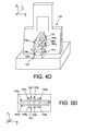
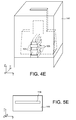
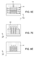
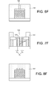
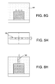
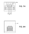
- FIGS. 5A-5H An exemplary method for producing a microelectronic device comprising a transistor having a semiconductor structure formed of a plurality of nano-wires, will now be described in connection with the Figures 4A-4F (representing a portion of the semiconductor structure in progress in a perspective view), the Figures 5A-5H (representing the semiconductor structure in progress according to a view from above), the Figures 6A-6H (representing the semiconductor structure in progress in a cross-sectional view B'B indicated in FIGS. 5A-5H), the Figures 7A-7H (representing the semiconductor structure in a cross-sectional view A'A shown in FIGS. 5A-5H), the Figures 8B-8H (Representing the semiconductor structure in a sectional view C'C shown in Figures 5B-5H).
- the starting material of the process may be a support 100 such as a substrate of the type commonly called “bulk” formed of a conductive support layer, or such as a semiconductor-on-insulator type substrate, for example of the type SOI ("SOI for" Silicon On Insulator “or sSOI (sSOI for” strained SOI "or SOI constrained) formed of a semiconductor layer for example based on Si covered with an insulating layer for example based on SiO 2 , itself covered with a thin semiconductor layer.
- SOI SOI for
- Si Silicon On Insulator
- sSOI sSOI for” strained SOI
- SOI constrained formed of a semiconductor layer for example based on Si covered with an insulating layer for example based on SiO 2 , itself covered with a thin semiconductor layer.
- stacks 103a, 103b, 103c of bars also called nano-son semiconductors (a single stack 103a being illustrated on FIG. Figure 4A , and on Figures 4B-4F following).
- These stacks 103a, 103b, 103c may each be formed of an alternation of bars or nanowires 104 1 , 104 2 , 104 3 , based on a first semiconductor material 105 such as for example silicon and bars or nano-son 106 1 , 106 2 , 106 3 , based on a second semiconductor material 107 such as for example Si x Ge y .
- the second semiconductor material 107 may have a germanium content, for example between 10 and 100%, preferably between 15% and 50% in order to allow good etch selectivity between the first semiconductor material 105 and the second semiconductor material 107.
- the first semiconductor material 105 may be constrained for example by voltage-constrained silicon, while the second semiconductor material 107 may be constrained for example by Si x Ge y constrained in compression.
- nanowire stacks it is possible first of all to produce a stack of semiconductor layers, formed for example by epitaxy, of an alternation of layers based on the first semiconductor material 105 and of layers based on of the second semiconductor material 107.
- the stack of layers is then etched through a masking, which may be a hard mask 108 based for example on silicon nitride such as Si 3 N 4 .
- the hard mask 108 is formed of several blocks 108a, 108b, 108c, having a constant cross section (the cross section being defined as a section taken in a plane parallel to the plane [o; i ; k ] of the orthogonal reference [o; i ; j ; k ] on the Figures 4A to 7A ).
- an etching which may be anisotropic, of the stack of semiconductor layers is carried out, so that the nano-wires of the stacks 103a, 103b, 103c , reproduce the shape of the blocks 108a, 108b, 108c, and also have a constant cross section.
- each stack 103a, 103b, 103c is provided with ends having a cross section substantially equal to or equal to that of its center.
- the nano-wires 104 1 , 106 1 , 104 2 , 106 2 , 104 3 , 106 3 , obtained at the end of this etching can thus have a parallelepipedal shape.
- the nano-wires 104 1 , 106 1 , 104 2 , 106 2 , 104 3 , 106 3 may also have a critical dimension dc, for example between 5 nanometers and 25 nanometers.
- critical dimension is meant throughout the description, the smallest dimension of a pattern except its thickness, the critical dimension being measured in a direction parallel to the main plane of the support (the main plane of the support, being defined on the Figures 4A and 7A as a plane parallel to the plane [o; i ; j ] an orthogonal reference [o; i ; j ; k ]).
- the nano-wires 104 1 , 106 1 , 104 2 , 106 2 , 104 3 , 106 3 may have a thickness e, for example between 2 nm and 50 nm (measured in a direction parallel to the vector k orthogonal reference [o; i ; j ; k ] on the Figure 4A ).
- the nano-wires 104 1 , 106 1 , 104 2 , 106 2 , 104 3 , 106 3 may also have a length, for example between 20 nm and 150 nm (measured in a direction parallel to the vector j orthogonal reference [O; i ; j ; k ] on the Figure 4A ) in particular for a grid length of between 10 and 100 nm.
- the total length of the nanowires is preferably greater than a minimum length corresponding to the cumulative gate length and twice the length of the contacts.
- a gate dielectric for example a gate oxide such as TEOS coated with at least one layer of gate material for example such as polysilicum.
- the grid stack thus produced on a central region of the stacks 103a, 103b, 103c, of nano-son, covers the top and side flanks of this central region of the stacks 103a, 103b, 103c.
- the gate stack may have a height (measured in a direction orthogonal to the support 100 and parallel to the vector k orthogonal reference [o; i ; j ; k ] on the Figures 4B , 6B, 8B ), greater than that of the stacks 103a, 103b, 103c of nano-son.
- This gate stack is then etched through a mask, which may be a hard mask 118 having a form of dummy gate, so as to form a sacrificial gate 110 covering the top and the lateral flanks of a central zone of the stacks 103a, 103b, 103c.
- a mask which may be a hard mask 118 having a form of dummy gate, so as to form a sacrificial gate 110 covering the top and the lateral flanks of a central zone of the stacks 103a, 103b, 103c.
- the hard mask 118 may have a thickness of, for example, between 10 nm and 100 nm and perhaps, for example, based on silicon nitride such as Si 3 N 4 .
- the sacrificial gate 110 may be formed with a length L (measured in a direction parallel to the vector j orthogonal reference [o; i ; j ; k ] on the Figures 4B and 6B ) for example between 10 nm and 150 nm.
- the length L of the sacrificial gate 110 may correspond to the critical dimension of the hard mask 118.
- the insulating zones 120a, 120b are spaced apart by a distance ⁇ corresponding to the length L of the sacrificial gate 110 (L and ⁇ being measured in a direction parallel to the vector j orthogonal reference [o; i ; j ; k ] on the Figures 4C and 5C ).
- the insulating zones 120a, 120b and the sacrificial gate 110 are thus made so as to cover and mask a central zone of each stack 103a, 103b, 103c, of nano-son semiconductors, these nano-wires having free ends, which are not covered with another material.
- the ends of the nanowires are in particular covered neither by the insulating zones 120a, 120b, nor by the hard masks 108, 118, or the sacrificial gate 110.
- the insulating zones 120a, 120b may be produced by deposition of an insulating layer, for example based on silicon nitride or a stack of layers formed of a silicon oxide layer and a nitride layer. of silicon on the support 100, up to the level of the hard mask 108 and by etching of this insulating layer.
- an insulating layer for example based on silicon nitride or a stack of layers formed of a silicon oxide layer and a nitride layer. of silicon on the support 100, up to the level of the hard mask 108 and by etching of this insulating layer.
- source areas 137 and drain 139 are formed.
- the first semiconductor material 105 at the ends of the nano-wires 104 1 , 104 2 , 104 3 based on the first semiconductor material 105 and / or a growth of the second semiconductor material 107 at the ends of the nano-wires 106 1 , 106 2 , 106 3 based on the second semiconductor material 107.
- the nano-wires 104 1 , 104 2 , 104 3 , 106 1 , 106 2 , 106 3 of the stacks 103a, 103b, 103c have wider free ends than at their portion. central covered by the sacrificial gate 110 and the insulating areas 120a, 120b. At the end of this step, the nanowires retain their critical dimension dc.
- the growth can be carried out so that the thickness E (measured in a direction parallel to the support 100 and the plane [o; i ; j ] of the orthogonal reference [o; i ; j ; k ] on the figure 4D ) of conductive material formed by growth on the nanowires may be for example between 10 nm and 50 nm.
- the dimensions of the source and drain areas are adjusted.
- a serrated profile can be implemented on the source and drain zones.
- This serrated profile can be obtained by using, during growth, a gas capable of selectively etching the second semiconductor material vis-à-vis the first semiconductor material.
- This gas may for example be HCl, in particular in the case where the second semiconductor material is SiGe.
- silane precursor for Si growth or a dichlorosilane and germane precursor for SiGe growth.
- Doping of the source 137 and drain 139 regions may also be performed. This doping can be carried out after growth, for example by boron-based ion implantation in the case where it is desired to make a PMOS type transistor, or based on phosphorus or arsenic, in the case where it is desired to carry out an NMOS type transistor.
- the doping can be carried out in situ at the time of epitaxial growth of the source and drain zones by incorporation of boron or phosphorus, for example.
- a masking layer 141 is formed on the support so as to cover the structure and the second hard mask 118.
- the masking layer 141 may be chosen based on a material that can be etched selectively with respect to that of the second hard mask 118. This masking layer 141 may be based on a silicon such as those commonly referred to as PMD ("PMD" for "Pre Metal Dielectric") generally used prior to steps of making metal elements.
- PMD Pre Metal Dielectric
- a removal step, for example by flattening or polishing CMP (CMP for "Chemical Mechanical Planarization"), of this masking layer 141 is then performed with a stop at the top of the second hard mask 118.
- the upper face or the top the hard mask 118 is thus revealed (e) at the end of this step of withdrawal ( Figures 4E, 5E , 6E, 7E 8E ). This may subsequently make it possible to remove this hard mask 118 without having to perform a photolithography step requiring alignment.
- an opening 145 is made, the bottom of which reveals the support, so as to reveal again the central portion of the stacks 103a, 103b, 103c.
- This opening 145 is first made by removing the second hard mask 118 covering the stacks 103a, 103b, 103c.
- the second hard mask 118 may be etched selectively with respect to the material of the masking layer 141 using, for example, a chemical etching based on TMAH (Tetramethylammonium hydroxide).
- TMAH Tetramethylammonium hydroxide
- the opening 145 made may have a constant section.
- the opening 145 made in the masking layer makes it possible to preserve the exact imprint of the sacrificial gate 110.
- the opening 145 formed in the masking layer 141 may have a layout and dimensions provided according to those of the insulating areas 120a, 120b.
- the opening 145 can thus have a critical dimension Dc equal to or substantially equal to the length L of the sacrificial gate 110 (the critical dimension Dc being measured in a direction parallel to the vector j orthogonal reference [o; i ; j ; k ] in Figures 1F and 2F).
- the opening 145 is then extended by also withdrawing portions of the sacrificial gate 110 situated above the stacks 103a, 103b, 103c of nanowires and against the lateral flanks of the nanowires in the central region of the stacks 103a, 103b, 103c. .
- the sacrificial gate 110 can be removed for example by wet etching with a solution of TMAH (tetramethylammonium hydroxide), with a stop on the sacrificial gate dielectric ( Figures 4F, 5F , 6F, 7F 8F ) which is then withdrawn into the opening 145.
- TMAH tetramethylammonium hydroxide
- a withdrawal of the second semiconductor material 107 selectively with respect to the first semiconductor material 105 can be realized, in particular if it is desired to make an NMOS type transistor.
- This selective shrinkage may be carried out, for example by chemical vapor-phase etching, for example using HCl mixed with a carrier gas or by chemical etching based on CF 4 , in the case where the material removed is Si x Ge y .
- nano-son suspended based on the first semiconductor material 105 in the opening 145, nano-son suspended based on the first semiconductor material 105.
- the nano-son 104 1 , 104 2 , 104 3 based on the first semiconductor material 105 can thus have a portion central cut off, in other words that is not covered with another material.
- the second semiconductor material 107 is preserved at the end of the nano-wires 104 1 , 104 2 , 104 3 , 106 1 , 106 2 , 106 3 , outside the opening 145.
- the nano-wires 104 1 , 104 2 , 104 3 based on the first semiconductor material 105 retain a critical dimension dc.
- a gate stack can be made conformably, for example using CVD deposition (CVD for "Chemical Vapor Deposition”), a gate dielectric for example based on HfO 2 , or HfSiON and at least one gate material, for example formed of a metal layer such as TiN or TaN and a layer of semiconductor material such as polysilicon, so as to fill the opening 145 .
- CVD deposition CVD for "Chemical Vapor Deposition”
- a gate dielectric for example based on HfO 2 , or HfSiON
- at least one gate material for example formed of a metal layer such as TiN or TaN and a layer of semiconductor material such as polysilicon, so as to fill the opening 145 .
- a coating grid 150 around a central portion of the nano-wires 104 1 , 104 2 , 104 3 of critical dimension dc is thus formed ( Figures 5H, 6H , 7H, 8H ).
- the grid 150 is formed around a central portion of the nano-wires 104 1 , 104 2 , 104 3 whose critical dimension dc is the same as after the production of the stacks described above in connection with the Figures 4A , 5A, 6A, 7A .
- a step of removing the gate material protruding above the opening 145 can then be performed.
- a grid having a gate length I (measured in a direction parallel to the vector j orthogonal reference [o; i ; j ; k ] on the figures 5H and 8H ) defined by the critical dimension Dc of the opening 145 is made.
- the gate 150 may have a constant length substantially equal to the distance ⁇ separating the insulating zones 120a, 120b from each other and the length L of the sacrificial gate 110 which has previously been removed can be obtained in this way.
- a first set of several stacks 103a, 103b, 103c of semiconductor nanowires and a second set of several stacks 203a, 203b, 203c, of semiconductor nano-wires are formed on a support 100.
- Stacks 103a, 103b, 103c, 203a, 203b, 203c each have a constant cross section with nanowires of critical dimension dc.
- the stacks 103a, 103b, 103c, 203a, 203b, 203c are each formed of an alternation of nano-wires 104 1 , 104 2 , 104 3 , based on a first semiconductor material 105 such as, for example, Si and nano-wires 106 1 , 106 2 , 106 3 , based on the second semiconductor material 107 such as for example Si x Ge y , by etching semiconductor layers through hard masks (not shown) .
- the sacrificial grids 110, 210 After having performed sacrificial grids 110, 210 on each set of stacks 103a, 103b, 103c, and 203a, 203b, 203c, nano-wires and spacing insulating zones (not shown) on the one hand and on the other hand, the sacrificial grids 110, 210 form the masking layer 141 covering the stacks 103a, 103b, 103c, and 203a, 203b, 203c and the sacrificial grids.
- the masking layer 141 can then be flattened until revealing the hard masks respectively covering the sacrificial grids 110 and 210.
- a first opening 145 is formed in the masking layer 141 ( Figure 9A ), so as to reveal a central region of the first set of stacks 103a, 103b, 103c, nano-son.
- This hard mask 243 may be, for example, polysilicon or silicon nitride or silicon oxide and thickness for example between 3 and 10 nm.
- the second semiconductor material 107 is then selectively removed from the first semiconductor material 105.
- This selective shrinkage can be carried out, for example, using HCl mixed with a carrier gas or by chemical etching. based on CF 4 .
- suspended nano-wires are obtained based on the first semiconductor material 105, for example based on silicon.
- a second opening 245 is then formed in the masking layer 141 to expose a central region of the second set of stacks 203a, 203b, 203c.
- the first opening 145 can, in turn, be filled at least partially with the aid of a protective mask stacks 103a, 103b, 103c.
- This protective mask can be made for example using a material that can be etched selectively vis-à-vis that of the masking layer 141, for example a material such as Si 3 N 4 used to form the hard mask (s).
- suspended nano-wires are obtained based on the second semiconductor material 107.
- the suspended nano-wires based on the second semiconductor material 107 retain the same critical dimension dc once they have been made. stacks.
- a grid stack is deposited in this opening 145.
- the first semiconductor material 105 is then selectively removed from the second semiconductor material 107 in a second opening 245 made in the masking layer 141 so as to reveal a central region of the second set of stacks 203a, 203b, 203c.
Landscapes
- Engineering & Computer Science (AREA)
- Chemical & Material Sciences (AREA)
- Nanotechnology (AREA)
- Physics & Mathematics (AREA)
- Crystallography & Structural Chemistry (AREA)
- Condensed Matter Physics & Semiconductors (AREA)
- General Physics & Mathematics (AREA)
- Manufacturing & Machinery (AREA)
- Mathematical Physics (AREA)
- Theoretical Computer Science (AREA)
- Thin Film Transistor (AREA)
- Materials Engineering (AREA)
Applications Claiming Priority (1)
| Application Number | Priority Date | Filing Date | Title |
|---|---|---|---|
| FR1253490A FR2989515B1 (fr) | 2012-04-16 | 2012-04-16 | Procede ameliore de realisation d'une structure de transistor a nano-fils superposes et a grille enrobante |
Publications (1)
| Publication Number | Publication Date |
|---|---|
| EP2654083A1 true EP2654083A1 (de) | 2013-10-23 |
Family
ID=48050617
Family Applications (1)
| Application Number | Title | Priority Date | Filing Date |
|---|---|---|---|
| EP13163838.9A Withdrawn EP2654083A1 (de) | 2012-04-16 | 2013-04-16 | Verbessertes Verfahren zur Herstellung einer Transistorstruktur mit übereinander angeordneten Nanokabeln mit Mantelgitter |
Country Status (3)
| Country | Link |
|---|---|
| US (1) | US8969148B2 (de) |
| EP (1) | EP2654083A1 (de) |
| FR (1) | FR2989515B1 (de) |
Cited By (4)
| Publication number | Priority date | Publication date | Assignee | Title |
|---|---|---|---|---|
| US9876121B2 (en) | 2015-03-16 | 2018-01-23 | Commissariat A L'energie Atomique Et Aux Energies Alternatives | Method for making a transistor in a stack of superimposed semiconductor layers |
| CN108933102A (zh) * | 2017-05-26 | 2018-12-04 | 台湾积体电路制造股份有限公司 | 基于纳米线的集成电路器件的间隔件及其制造方法 |
| US10217849B2 (en) | 2016-12-15 | 2019-02-26 | Commissariat A L'energie Atomique Et Aux Energies Alternatives | Method for making a semiconductor device with nanowire and aligned external and internal spacers |
| TWI716441B (zh) * | 2015-09-03 | 2021-01-21 | 美商應用材料股份有限公司 | 用於製造對於半導體應用的水平環繞式閘極裝置的奈米線的方法 |
Families Citing this family (22)
| Publication number | Priority date | Publication date | Assignee | Title |
|---|---|---|---|---|
| US9396984B2 (en) | 2012-09-05 | 2016-07-19 | Commissariat A L'energie Atomique Et Aux Energies Alternatives | Method of producing a microelectronic device in a monocrystalline semiconductor substrate with isolation trenches partially formed under an active region |
| US9595525B2 (en) * | 2014-02-10 | 2017-03-14 | International Business Machines Corporation | Semiconductor device including nanowire transistors with hybrid channels |
| US9543440B2 (en) * | 2014-06-20 | 2017-01-10 | International Business Machines Corporation | High density vertical nanowire stack for field effect transistor |
| US9502518B2 (en) | 2014-06-23 | 2016-11-22 | Stmicroelectronics, Inc. | Multi-channel gate-all-around FET |
| US9343529B2 (en) * | 2014-09-05 | 2016-05-17 | International Business Machines Corporation | Method of formation of germanium nanowires on bulk substrates |
| US9576856B2 (en) * | 2014-10-27 | 2017-02-21 | Globalfoundries Inc. | Fabrication of nanowire field effect transistor structures |
| US9909453B2 (en) | 2015-05-19 | 2018-03-06 | General Electric Company | Lubrication system for a turbine engine |
| US10415429B2 (en) | 2015-09-25 | 2019-09-17 | General Electric Company | Planet gearbox with cylindrical roller bearing with high density roller packing |
| US10234018B2 (en) | 2015-10-19 | 2019-03-19 | General Electric Company | Planet gearbox with cylindrical roller bearing with under race lube scheme |
| FR3043837B1 (fr) | 2015-11-17 | 2017-12-15 | Commissariat Energie Atomique | Procede de realisation de transistor a nanofil semi-conducteur et comprenant une grille et des espaceurs auto-alignes |
| ITUB20156062A1 (it) | 2015-12-01 | 2017-06-01 | Gen Electric | Alloggiamento per l'uso in un motore a turboventilatore e procedimento di lavaggio di fluido da esso. |
| FR3051970B1 (fr) | 2016-05-25 | 2020-06-12 | Commissariat A L'energie Atomique Et Aux Energies Alternatives | Realisation d'une structure de canal formee d'une pluralite de barreaux semi-conducteurs contraints |
| US10236362B2 (en) * | 2016-06-30 | 2019-03-19 | International Business Machines Corporation | Nanowire FET including nanowire channel spacers |
| CN108735804B (zh) * | 2017-04-25 | 2021-05-14 | 中芯国际集成电路制造(上海)有限公司 | 晶体管及其制作方法 |
| EP3425673A1 (de) * | 2017-07-04 | 2019-01-09 | IMEC vzw | Germaniumnanodrahtherstellung |
| CN108598170B (zh) * | 2018-05-24 | 2022-07-08 | 厦门半导体工业技术研发有限公司 | 纳米线晶体管及其制作方法 |
| US11367783B2 (en) | 2018-08-17 | 2022-06-21 | Taiwan Semiconductor Manufacturing Co., Ltd. | Method of manufacturing a semiconductor device |
| US11217694B2 (en) * | 2019-03-18 | 2022-01-04 | Shanghai Industrial Μtechnology Research Institute | Field-effect transistor and method for manufacturing the same |
| US11456368B2 (en) * | 2019-08-22 | 2022-09-27 | Taiwan Semiconductor Manufacturing Co., Ltd. | Semiconductor device structure with hard mask layer over fin structure and method for forming the same |
| US11257917B2 (en) | 2020-06-05 | 2022-02-22 | Qualcomm Incorporated | Gate-all-around (GAA) transistors with additional bottom channel for reduced parasitic capacitance and methods of fabrication |
| FR3123502B1 (fr) | 2021-05-27 | 2024-01-05 | Commissariat Energie Atomique | Procédé de fabrication d'un transistor a structure de grille enrobante |
| US12421898B2 (en) | 2022-06-22 | 2025-09-23 | General Electric Company | Gearbox assembly with lubricant extraction volume ratio |
Citations (6)
| Publication number | Priority date | Publication date | Assignee | Title |
|---|---|---|---|---|
| US20060071275A1 (en) * | 2004-09-30 | 2006-04-06 | Brask Justin K | Nonplanar transistors with metal gate electrodes |
| US20060216897A1 (en) | 2005-03-24 | 2006-09-28 | Samsung Electronics Co., Ltd. | Semiconductor device having a round-shaped nano-wire transistor channel and method of manufacturing same |
| WO2008069765A1 (en) | 2006-12-08 | 2008-06-12 | Agency For Science, Technology And Research | A stacked silicon-germanium nanowire structure and a method of forming the same |
| WO2010090978A1 (en) | 2009-02-04 | 2010-08-12 | International Business Machines Corporation | Maskless process for suspending and thinning nanowires |
| US20100295021A1 (en) * | 2009-05-21 | 2010-11-25 | International Business Machines Corporation | Single Gate Inverter Nanowire Mesh |
| US20110281412A1 (en) | 2005-12-30 | 2011-11-17 | Commissariat A L'energie Atomique | Production of a transistor gate on a multibranch channel structure and means for isolating this gate from the source and drain regions |
Family Cites Families (5)
| Publication number | Priority date | Publication date | Assignee | Title |
|---|---|---|---|---|
| KR100481209B1 (ko) | 2002-10-01 | 2005-04-08 | 삼성전자주식회사 | 다중 채널을 갖는 모스 트랜지스터 및 그 제조방법 |
| JP2008303167A (ja) | 2007-06-07 | 2008-12-18 | Sony Chemical & Information Device Corp | 新規なスルホニウムボレート錯体 |
| FR2937463B1 (fr) | 2008-10-17 | 2010-12-24 | Commissariat Energie Atomique | Procede de fabrication de composants empiles et auto-alignes sur un substrat |
| US9029834B2 (en) * | 2010-07-06 | 2015-05-12 | International Business Machines Corporation | Process for forming a surrounding gate for a nanowire using a sacrificial patternable dielectric |
| US8753942B2 (en) * | 2010-12-01 | 2014-06-17 | Intel Corporation | Silicon and silicon germanium nanowire structures |
-
2012
- 2012-04-16 FR FR1253490A patent/FR2989515B1/fr active Active
-
2013
- 2013-04-15 US US13/862,830 patent/US8969148B2/en active Active
- 2013-04-16 EP EP13163838.9A patent/EP2654083A1/de not_active Withdrawn
Patent Citations (6)
| Publication number | Priority date | Publication date | Assignee | Title |
|---|---|---|---|---|
| US20060071275A1 (en) * | 2004-09-30 | 2006-04-06 | Brask Justin K | Nonplanar transistors with metal gate electrodes |
| US20060216897A1 (en) | 2005-03-24 | 2006-09-28 | Samsung Electronics Co., Ltd. | Semiconductor device having a round-shaped nano-wire transistor channel and method of manufacturing same |
| US20110281412A1 (en) | 2005-12-30 | 2011-11-17 | Commissariat A L'energie Atomique | Production of a transistor gate on a multibranch channel structure and means for isolating this gate from the source and drain regions |
| WO2008069765A1 (en) | 2006-12-08 | 2008-06-12 | Agency For Science, Technology And Research | A stacked silicon-germanium nanowire structure and a method of forming the same |
| WO2010090978A1 (en) | 2009-02-04 | 2010-08-12 | International Business Machines Corporation | Maskless process for suspending and thinning nanowires |
| US20100295021A1 (en) * | 2009-05-21 | 2010-11-25 | International Business Machines Corporation | Single Gate Inverter Nanowire Mesh |
Cited By (6)
| Publication number | Priority date | Publication date | Assignee | Title |
|---|---|---|---|---|
| US9876121B2 (en) | 2015-03-16 | 2018-01-23 | Commissariat A L'energie Atomique Et Aux Energies Alternatives | Method for making a transistor in a stack of superimposed semiconductor layers |
| TWI716441B (zh) * | 2015-09-03 | 2021-01-21 | 美商應用材料股份有限公司 | 用於製造對於半導體應用的水平環繞式閘極裝置的奈米線的方法 |
| US10217849B2 (en) | 2016-12-15 | 2019-02-26 | Commissariat A L'energie Atomique Et Aux Energies Alternatives | Method for making a semiconductor device with nanowire and aligned external and internal spacers |
| CN108933102A (zh) * | 2017-05-26 | 2018-12-04 | 台湾积体电路制造股份有限公司 | 基于纳米线的集成电路器件的间隔件及其制造方法 |
| CN108933102B (zh) * | 2017-05-26 | 2020-10-16 | 台湾积体电路制造股份有限公司 | 基于纳米线的集成电路器件的间隔件及其制造方法 |
| US10825915B2 (en) | 2017-05-26 | 2020-11-03 | Taiwan Semiconductor Manufacturing Co., Ltd. | Spacers for nanowire-based integrated circuit device and method of fabricating same |
Also Published As
| Publication number | Publication date |
|---|---|
| US8969148B2 (en) | 2015-03-03 |
| FR2989515A1 (fr) | 2013-10-18 |
| FR2989515B1 (fr) | 2015-01-16 |
| US20130302955A1 (en) | 2013-11-14 |
Similar Documents
| Publication | Publication Date | Title |
|---|---|---|
| EP2654083A1 (de) | Verbessertes Verfahren zur Herstellung einer Transistorstruktur mit übereinander angeordneten Nanokabeln mit Mantelgitter | |
| FR3090998A1 (fr) | Architecture à transistors n et p superposes a structure de canal formee de nanofils | |
| FR3086456A1 (fr) | Procede de realisation de transistors superposes | |
| EP2254146B1 (de) | Halbleiterstruktur und Herstellungsverfahren für eine Halbleiterstruktur | |
| EP3070744B1 (de) | Verbessertes herstellungsverfahren eines transistors in einem stapel von übereinander angeordneten halbleiterschichten | |
| EP3701567B1 (de) | Verfahren zur herstellung eines elektronischen bauteils mit doppelquantenpunkten | |
| FR3060839A1 (fr) | Procede de realisation d'un dispositif semi-conducteur a nanofil et espaceurs externe et interne alignes | |
| FR3016237A1 (fr) | Dispositif a nanofils de semi-conducteur partiellement entoures par une grille | |
| FR3060838A1 (fr) | Procede de realisation d'un dispositif semi-conducteur a canal contraint en compression | |
| EP3502049B1 (de) | Herstellungsverfahren einer halbleitervorrichtung, die eine oder mehrere nanostrukturen umfasst | |
| FR3043837A1 (fr) | Procede de realisation de transistor a nanofil semi-conducteur et comprenant une grille et des espaceurs auto-alignes | |
| FR3005309A1 (fr) | Transistors a nanofils et planaires cointegres sur substrat soi utbox | |
| WO2006131615A1 (fr) | Transistor a canal a base de germanium enrobe par une electrode de grille et procede de fabrication d'un tel transistor | |
| EP1690297B1 (de) | Mikroelektronische feldeffekteinrichtung mit der fähigkeit zur bildung eines oder mehrerer transistorkanäle | |
| EP1869712A1 (de) | Struktur und verfahren zur realisierung einer mit einer anzahl von quantenleitungen ausgestatteten mikroelektronischen einrichtung mit der fähigkeit zur bildung eines oder mehrerer transistorkanäle | |
| EP4187612A1 (de) | Herstellung einer quantenvorrichtung mit selbstausgerichteter gate-anordnung auf ihre jeweiligen aktiven gebietsregion | |
| FR3050867A1 (fr) | Procede de fabrication d'un transistor a nanocouches a canal vertical | |
| EP3511293A1 (de) | Herstellungsverfahren mindestens eines feldeffekttransistors | |
| EP3062350B1 (de) | Verfahren zur veränderung des spannungszustands einer halbleiterstruktur mit transistorkanalstufen | |
| EP1788635B1 (de) | Verfahren zum Herstellen eines Transistors mit selbst justierten Doppel-Gates durch Schrumpfung der Gatestruktur | |
| FR3070089A1 (fr) | Procede de formation de regions d'extension dopees dans une structure a nanofils superposes | |
| EP1433206B1 (de) | Ein-elektron-transistor mit einem vertikalkanal, und herstellungsverfahren dafür | |
| FR3069952B1 (fr) | Realisation d'un transistor a structure de canal et regions de source et de drain en semi-metal | |
| EP3104402B1 (de) | Herstellung von selbstausgerichteten verbindungselementen für integrierten 3d-schaltkreis | |
| FR3085085A1 (fr) | Transistor a barreaux superposes et structure double-grille |
Legal Events
| Date | Code | Title | Description |
|---|---|---|---|
| PUAI | Public reference made under article 153(3) epc to a published international application that has entered the european phase |
Free format text: ORIGINAL CODE: 0009012 |
|
| AK | Designated contracting states |
Kind code of ref document: A1 Designated state(s): AL AT BE BG CH CY CZ DE DK EE ES FI FR GB GR HR HU IE IS IT LI LT LU LV MC MK MT NL NO PL PT RO RS SE SI SK SM TR |
|
| AX | Request for extension of the european patent |
Extension state: BA ME |
|
| 17P | Request for examination filed |
Effective date: 20131223 |
|
| RBV | Designated contracting states (corrected) |
Designated state(s): AL AT BE BG CH CY CZ DE DK EE ES FI FR GB GR HR HU IE IS IT LI LT LU LV MC MK MT NL NO PL PT RO RS SE SI SK SM TR |
|
| STAA | Information on the status of an ep patent application or granted ep patent |
Free format text: STATUS: THE APPLICATION IS DEEMED TO BE WITHDRAWN |
|
| 18D | Application deemed to be withdrawn |
Effective date: 20151031 |