EP2656436B1 - Appareil d'antenne hélicoïdale et procédé de formation d'une antenne hélicoïdale - Google Patents
Appareil d'antenne hélicoïdale et procédé de formation d'une antenne hélicoïdale Download PDFInfo
- Publication number
- EP2656436B1 EP2656436B1 EP11811441.2A EP11811441A EP2656436B1 EP 2656436 B1 EP2656436 B1 EP 2656436B1 EP 11811441 A EP11811441 A EP 11811441A EP 2656436 B1 EP2656436 B1 EP 2656436B1
- Authority
- EP
- European Patent Office
- Prior art keywords
- dielectric core
- antenna
- chassis
- circuit board
- printed circuit
- Prior art date
- Legal status (The legal status is an assumption and is not a legal conclusion. Google has not performed a legal analysis and makes no representation as to the accuracy of the status listed.)
- Active
Links
Images


Classifications
-
- H—ELECTRICITY
- H01—ELECTRIC ELEMENTS
- H01Q—ANTENNAS, i.e. RADIO AERIALS
- H01Q1/00—Details of, or arrangements associated with, antennas
- H01Q1/36—Structural form of radiating elements, e.g. cone, spiral, umbrella; Particular materials used therewith
-
- H—ELECTRICITY
- H01—ELECTRIC ELEMENTS
- H01Q—ANTENNAS, i.e. RADIO AERIALS
- H01Q1/00—Details of, or arrangements associated with, antennas
- H01Q1/12—Supports; Mounting means
- H01Q1/22—Supports; Mounting means by structural association with other equipment or articles
- H01Q1/24—Supports; Mounting means by structural association with other equipment or articles with receiving set
-
- H—ELECTRICITY
- H01—ELECTRIC ELEMENTS
- H01Q—ANTENNAS, i.e. RADIO AERIALS
- H01Q1/00—Details of, or arrangements associated with, antennas
- H01Q1/36—Structural form of radiating elements, e.g. cone, spiral, umbrella; Particular materials used therewith
- H01Q1/362—Structural form of radiating elements, e.g. cone, spiral, umbrella; Particular materials used therewith for broadside radiating helical antennas
-
- H—ELECTRICITY
- H01—ELECTRIC ELEMENTS
- H01Q—ANTENNAS, i.e. RADIO AERIALS
- H01Q1/00—Details of, or arrangements associated with, antennas
- H01Q1/36—Structural form of radiating elements, e.g. cone, spiral, umbrella; Particular materials used therewith
- H01Q1/38—Structural form of radiating elements, e.g. cone, spiral, umbrella; Particular materials used therewith formed by a conductive layer on an insulating support
-
- H—ELECTRICITY
- H04—ELECTRIC COMMUNICATION TECHNIQUE
- H04R—LOUDSPEAKERS, MICROPHONES, GRAMOPHONE PICK-UPS OR LIKE ACOUSTIC ELECTROMECHANICAL TRANSDUCERS; ELECTRIC HEARING AIDS; PUBLIC ADDRESS SYSTEMS
- H04R1/00—Details of transducers, loudspeakers or microphones
- H04R1/08—Mouthpieces; Microphones; Attachments therefor
- H04R1/083—Special constructions of mouthpieces
-
- H—ELECTRICITY
- H04—ELECTRIC COMMUNICATION TECHNIQUE
- H04R—LOUDSPEAKERS, MICROPHONES, GRAMOPHONE PICK-UPS OR LIKE ACOUSTIC ELECTROMECHANICAL TRANSDUCERS; ELECTRIC HEARING AIDS; PUBLIC ADDRESS SYSTEMS
- H04R2420/00—Details of connection covered by H04R, not provided for in its groups
- H04R2420/07—Applications of wireless loudspeakers or wireless microphones
-
- Y—GENERAL TAGGING OF NEW TECHNOLOGICAL DEVELOPMENTS; GENERAL TAGGING OF CROSS-SECTIONAL TECHNOLOGIES SPANNING OVER SEVERAL SECTIONS OF THE IPC; TECHNICAL SUBJECTS COVERED BY FORMER USPC CROSS-REFERENCE ART COLLECTIONS [XRACs] AND DIGESTS
- Y10—TECHNICAL SUBJECTS COVERED BY FORMER USPC
- Y10T—TECHNICAL SUBJECTS COVERED BY FORMER US CLASSIFICATION
- Y10T29/00—Metal working
- Y10T29/49—Method of mechanical manufacture
- Y10T29/49002—Electrical device making
- Y10T29/49016—Antenna or wave energy "plumbing" making
- Y10T29/49018—Antenna or wave energy "plumbing" making with other electrical component
Definitions
- the disclosure herein relates to the field of small broadband antennas, and more particularly to helical antennas that may be used with wireless microphones that transmit in the UHF band range.
- Kenkel discloses a helical antenna assembly formed by taking a non-metallic tape and placing a metallic tape strip diagonally onto the non-metallic tape. A dielectric core is then wrapped with the tape. An electrical connector and a central conductor that is located in the center of the dielectric core contact the metallic tape strip. One or two tabs on the tape are bent over the ends of the dielectric core to prevent the tape assembly from separating from the dielectric core. Eyelets are also affixed to the center conductor to pin the tabs. The pitch and width of the conductive portion of the tape assembly can be altered to obtain the desired electrical characteristics when the tape assembly is wrapped around the dielectric core.
- the present invention provides an antenna assembly comprising: a dielectric core comprising a shock absorbing material; an antenna tape wrapped around the dielectric core, the tape comprising a conductive portion; and a printed circuit board, wherein the printed circuit board and the conductive portion on the tape are electrically coupled, characterised in that the printed circuit board extends from a chassis, and the dielectric core is configured to extend into the chassis; wherein the dielectric core has a first portion and a second portion, the first portion configured to receive the antenna tape and the second portion being configured to be inserted into the chassis.
- the present invention provides a method for forming an antenna comprising: forming a dielectric core of a shock absorbing material, comprising forming the dielectric core with a first portion and a second portion; wrapping an antenna tape around the dielectric core, comprising wrapping the antenna tape around the first portion, the antenna tape comprising a conductive portion; electrically coupling a printed circuit board and the conductive portion, mounting the printed circuit board to a chassis at a point located away from the chassis; and placing the dielectric core into the chassis, comprising inserting the second portion into the chassis.
- FIGS. 1 and 2 generally depict an antenna 100 having a dielectric core 130 with an antenna wrap or tape 120, a printed circuit board ("PCB") 110, and an antenna cover 114.
- the antenna 100 is secured to a chassis 104 of a handheld microphone.
- the handheld microphone can include a wireless transmitter for wireless transmission.
- the microphone generally has a transducer element or sound capsule for receiving sound input.
- the transducer element can be dynamic, condenser, ribbon, or any other known transducer element.
- a conductive element such as a coupling wire 106 or flex cable (not shown) may electrically couple a conductive portion 122 of the antenna tape 120 to the PCB 110, which acts as a strain relief connection interface between the two components.
- a ground element which can be a screw 112, may be used to connect the PCB 110 to the chassis 104 near the wire 106 to allow for a proper ground reference.
- the dielectric core 130 can mount near the PCB 110 and in the chassis 104.
- the PCB 110 extends past a chassis wall 105 and into an opening 144 of a handheld microphone.
- a shock absorbing member 146 comprising a small piece of shock absorbing foam can be placed between the inside area of the antenna cover 114 and the end of the dielectric core 130 to provide additional shock absorption capability to absorb shock energy during drop impact if the antenna is mishandled.
- the shock absorbing member 146 can be formed of a poron pad.
- the coupling wire 106 provides strain relief between the PCB 110 and the antenna 100.
- the coupling wire 106 can be provided with extra length so as to provide additional slack in the wire such that it can freely move during drop impact without being severed. This enhances the shock absorption capabilities of the antenna 100 if it is dropped or mishandled, or if the antenna 100 is otherwise moved relative to the PCB 110.
- the radio frequency (“RF") signal needs to be properly referenced to a ground.
- the ground screw 112 can be added between the chassis 104 and the PCB 110 to act as the ground reference.
- the chassis 104 is provided with an L-shaped tab or flange 116 that extends from the chassis 104 for retaining the PCB 110.
- the PCB 110 is secured to the tab 116 by ground screw 112 at a point away from the chassis 104. This allows the PCB 110 to extend further out of the chassis 104 of the microphone and to provide a shorter distance between the antenna 100 and the PCB 110, which ultimately provides a better RF transmission to the antenna 100.
- the chassis 104 can be provided with threads 118 for receiving mating threads on a sleeve 148 which serves as an external handle or grip on the wireless microphone, and may also serve as an exterior housing covering batteries for operating the microphone.
- One or more screws 140 align with screw holes 142 to maintain the antenna cover 114 and the dielectric core 130 in place on the chassis 104. However, other methods for securing the antenna cover 114 to the chassis 104 are also contemplated.
- FIGS. 5 and 6 generally depict one embodiment of a dielectric core 130.
- FIG. 5 shows the dielectric core 130 prior to being wrapped with antenna tape 120
- FIG. 6 shows the dielectric core 130 after being wrapped with antenna tape 120.
- the dielectric core 130 is not rigid and helps absorb drop stress to protect the PCB 110 and the electrical contacts in the antenna 100.
- a suitable material for forming the dielectric core 130 is Thermoplastic Urethane ("TPU”), which provides good absorption of shock energy during drop impact of the antenna 100.
- TPU Thermoplastic Urethane
- the dielectric core 130 has a first cylindrical portion 132 and a second elongated portion 134.
- the first cylindrical portion 132 is configured to receive the antenna tape 120
- the second elongated portion 134 is configured to be inserted into the chassis 104 of the microphone.
- the first cylindrical portion 132 may have a circular cross section for receiving the antenna tape 100.
- the second elongated portion 134 may have a D-shaped cross section or a partially curved profile with a flat surface for interfacing with the L-shaped tab 116 of the chassis 104 and the PCB 110 such that the dielectric core 130 does not interfere with the PCB 110 during assembly.
- the D-shaped profile corresponds to the inside profile of the chassis 104 formed by the opening 144 in the chassis 104, the tab 116, and the PCB 110, and allows the dielectric core 130 to be placed in the chassis 104 around the tab 116 and PCB 110.
- the addition of the second elongated portion 134 provides good shock absorption properties to the antenna 100.
- the second elongated portion 134 also has an opening 133 which may extend throughout the length of the second elongated portion 134, and to the first cylindrical portion 132.
- the second elongated portion 134 is also provided with two holes 136 for securing the dielectric core 130 and the antenna cover 114 to the chassis 104 via one or more screws 140.
- a notch 138 in the second elongated portion 134 provides a recess which provides clearance between an end of the ground screw 112 and the dielectric core 130. This permits the ground screw 112 to fully extend past the tab 116 of the chassis 104 without contacting the dielectric core 130, such that the screw 112 does not impact the positioning of the dielectric core 130 relative to the PCB 110.
- the two holes 136 can be formed suitable for mating to screws 140, which can be self tapping (shown in FIG. 3 ). This provides a low cost mating mechanical connection interface to the chassis 104.
- the dielectric core 130 can be modified into other shapes and configurations.
- the first portion 132A can be formed into to an elliptical shape to account for other required mechanical features.
- FIGS. 7A-7C depict antenna tapes 120A, 120B, 120C that may be used in conjunction with the antenna 100 and the dielectric core 130.
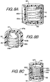
- FIGS. 8A-8C respectively show the antenna tapes of FIGS. 7A-7C wrapped around the dielectric core 130.
- the antenna tapes 120A, 120B, 120C can comprise conductive portions 122A, 122B, 122C and substrate portions 124A, 124B, 124C.
- the conductive portions 122A, 122B, 122C can be formed of copper foil and the substrate portions 124A, 124B, 124C can be formed of polyester material having an adhesive backing. However, other materials are also contemplated.
- the antenna tapes 120A, 120B, 120C can be formed by attaching the conductive portions 122A, 122B, 122C to the substrate portions 124A, 124B, 124C by any known method.
- the dimensions, lengths, orientations, shapes, etc. of the conductive portions 122A, 122B, 122C can be configured to optimize antenna performance.
- the conductive portion 122A can be formed with a first horizontal portion 126A, an inclined portion 128A, and a second substantially horizontal upper portion 129A to provide the proper transmission characteristics.
- FIG. 7B An alternative embodiment is shown in FIG. 7B .
- This embodiment is similar to the embodiment shown in FIG. 7A in that the conductive portion 122B has a first horizontal portion 126B, an inclined portion 128B, and a second substantially horizontal upper portion 129B; however, the conductive portion 122B is formed with a vertical portion 125B formed approximately at a right angle to the first horizontal portion 126B and a top element 127B positioned off of the second substantially horizontal upper portion 129B formed into a circular shape.
- This antenna-tape design may improve performance of the microphone at lower frequency band transmission.
- the conductive portions 122A, 122B can be dimensioned 0.100 in. or 2.54 mm in width with the exception of the top element 127B which is formed of a larger diameter.
- the top element 127B which is formed of a larger diameter.
- other dimensions may also provide the proper performance characteristics of the antenna 100.
- the conductive portion 122C can be formed with a first conductive element 123C and a second conductive element 125C formed at an incline both following substantially straight lines.
- the first conductive element 123C and the second conductive element 125C can intersect at the bottom of the antenna tape 120C.
- the conductive portion 122C is formed with a vertical portion 126C formed approximately at a right angle to the antenna tape 120C near the intersection of the first conductive element 123C and the second conductive element 125C.
- Two top vertical portions 127C can be formed approximately at right angles to the antenna tape 120C to form a connection between the first conductive element 123C and the second conductive element 125C when the antenna tape 120C is wrapped around the dielectric core 130. Additionally, in an alternative exemplary embodiment, a round top element (not shown) similar to the top element 127B shown in FIG. 7B can be formed near the top of the first conductive element 123C and the second conductive element 125C to form the contact between the two elements.
- the antenna 100 could be formed on a piece of flexible PCB or be formed as part of the PCB 110 and wrapped onto the dielectric core 130 after the PCB 110 is assembled into the chassis 104.
- the conductive portion 122 on the antenna tape 120 is just a trace of specific length and pitch, it could be fabricated as part of the PCB 110.
- an adhesive backer could be added to the antenna tape 120 to allow for it to be wrapped onto the dielectric core 130. This would eliminate the solder operations associated with connecting the wire 106 to the PCB 110 and the conductive portion 122 and their associated costs but may add costs due to PCB material utilization.
- FIG. 8A illustrates the antenna tape 120A shown in FIG. 7A wrapped around the first cylindrical portion 132 of the dielectric core 130. As shown in FIG. 8 , the conductive portion 122A wraps around the dielectric core 130 two and a half times.
- FIG. 8B illustrates the antenna tape 120B wrapped around the first cylindrical portion 132 of the dielectric core 130.
- the conductive portion 122B wraps around the dielectric core 130 about two and a half times. Additionally, the vertical portion 125B folds down over the bottom of the dielectric core 130, and the top element 127B folds over the top of the first cylindrical portion 132 of the dielectric core 130.
- FIG. 8C illustrates the antenna tape 120C wrapped around the first cylindrical portion 132 of the dielectric core 130.
- the first and second elements 123C, 125C form a double helix surrounding the dielectric core 130.
- the first conductive element 123C and the second conductive element 125C each wrap around the dielectric core 130 about two times. This forms a helical antenna wrapped up the dielectric core 130 corresponding to the first conductive element 123C, then across the top face of the dielectric core 130 via the two top vertical portions 127C, and a second helical wrapping down the dielectric core 130 corresponding to the second conductive element 125C.
- both the first conductive element 123C, which forms an upward helical wrap in a first direction and the second conductive element 125C, which forms a downward helical wrap in the opposite direction will both be terminated on the RF feed from the PCB 110.
- Both the first conductive element 123C and the second conductive element 125C can be connected to the RF feed on the PCB 110 in operation, which is different than the embodiments shown in FIGS. 7A and 7B because the conductive element 122C is terminated back to the RF feed on the PCB 110.
- the second conductive element 125C could be tied to ground instead of the RF feed on the PCB 110.
- the dielectric core 130 is wrapped with the antenna tape 120.
- the PCB 110 is next secured to the L-shaped tab 116 of the chassis 104 by the screw 112.
- the ground screw 112 When the ground screw 112 is installed, it compresses an electrically conductive area on the PCB 110 against an electrically conductive area on the L-shaped tab 116 where the paint or finish has been masked, forming an electrical ground connection to provide RF grounding between the PCB 110 and the chassis 104.
- a solder mask can be removed near the screw hole and a paste can be added to increase the contact area and consistency of the ground reference.
- the coupling wire 106 or flex cable can then be soldered to the PCB 110 with either a copper pad or a copper-plated through hole on the PCB 110.
- the wire 106 or flex cable can then be soldered to the conductive portion 122 on the antenna tape 120.
- the dielectric core 130 is inserted into the chassis 104 and the antenna cover 114 is placed over the dielectric core 130. Both the dielectric core 130 and the antenna cover 114 are secured to the chassis 104 by two self-taping screws 140 that are inserted through the antenna cover 114 and into the holes 136 in the second elongated portion 134 of the dielectric core 130.
- a rigid-flex can be used to extend from the PCB 110 and the end of the rigid-flex can be plated with copper. This plated rigid flex is then soldered directly to the conductive portion of the antenna removing the necessity of the coupling wire 106 and, therefore, eliminates having to solder the coupling wire 106 or flex cable to the antenna 100 and the PCB 110.
- the antenna embodiments disclosed herein may achieve a 13% fractional bandwidth over 470-950MHz with tuning by changing the conductor length while fitting into a small microphone chassis.
- the embodiments disclosed herein can be implemented in any future handheld wireless device, including but not limited to, devices operating in a similar frequency band that utilize a metal chassis and an antenna cover.
Landscapes
- Details Of Aerials (AREA)
- Support Of Aerials (AREA)
Claims (16)
- Ensemble d'antenne comprenant :un coeur diélectrique (130) comprenant un matériau d'absorption de chocs ;un ruban d'antenne (120) enroulé autour du coeur diélectrique, le ruban comprenant une partie conductrice (122) ; etune carte de circuit imprimé (110), dans lequel la carte de circuit imprimé et la partie conductrice sur le ruban sont couplées électriquement,caractérisé en ce que la carte de circuit imprimé s'étend depuis un châssis (104), et le coeur diélectrique est configuré pour s'étendre dans le châssis ;
dans lequel le coeur diélectrique a une première partie (132) et une seconde partie (134), la première partie étant configurée pour recevoir le ruban d'antenne et la seconde partie étant configurée pour être insérée dans le châssis. - Ensemble d'antenne selon la revendication 1, dans lequel la première partie a une section transversale circulaire ou elliptique et la seconde partie a une section transversale en forme de D.
- Ensemble d'antenne selon la revendication 2, dans lequel le coeur diélectrique a une ouverture (133) dans la seconde partie et la seconde partie a au moins un trou (136) pour recevoir un élément de fixation afin de fixer le coeur diélectrique au châssis.
- Ensemble d'antenne selon la revendication 1, dans lequel un élément conducteur (106) couple électriquement la carte de circuit imprimé et la partie conductrice.
- Ensemble d'antenne selon la revendication 4, dans lequel l'élément conducteur comprend un fil qui est soudé à la fois à la carte de circuit imprimé et à la partie conductrice.
- Ensemble d'antenne selon la revendication 1, comprenant en outre un couvercle d'antenne (114) positionné sur le coeur diélectrique et un élément d'absorption de chocs positionné entre le coeur diélectrique et le couvercle d'antenne.
- Ensemble d'antenne selon la revendication 1, dans lequel la carte de circuit imprimé monte sur une patte (116) s'étendant depuis le châssis et dans lequel un élément de mise à la terre fournit un contact électrique entre la carte de circuit imprimé et la patte pour mettre l'antenne à la terre.
- Ensemble d'antenne selon la revendication 7, dans lequel l'élément de mise à la terre comprend une vis (112).
- Ensemble d'antenne selon la revendication 1, dans lequel la partie conductrice comprend un premier élément conducteur (123C) et un second élément conducteur (125C) qui forment une double hélice autour du coeur diélectrique.
- Ensemble d'antenne selon la revendication 1, dans lequel la partie conductrice comprend un élément supérieur (127B ; 127C) positionné sur une extrémité du coeur diélectrique.
- Ensemble d'antenne selon la revendication 1, dans lequel au moins une partie de la carte de circuit imprimé est située dans le châssis.
- Procédé de formation d'une antenne comprenant :la formation d'un coeur diélectrique d'un matériau d'absorption de chocs, comprenant la formation du coeur diélectrique avec une première partie (132) et une seconde partie (134) ;l'enroulement d'un ruban d'antenne (120) autour du coeur diélectrique (130), comprenant l'enroulement du ruban d'antenne autour de la première partie, le ruban d'antenne comprenant une partie conductrice (122) ;le couplage électrique d'une carte de circuit imprimé (110) et de la partie conductrice,le montage de la carte de circuit imprimé sur un châssis (104) sur un point situé loin du châssis ; etle placement du coeur diélectrique dans le châssis, comprenant l'insertion de la seconde partie dans le châssis.
- Procédé selon la revendication 12, comprenant en outre la fixation du coeur diélectrique au châssis avec un élément de fixation.
- Procédé selon la revendication 12, comprenant en outre le soudage d'un élément conducteur (106) à la fois sur la carte de circuit imprimé et la partie conductrice et la fixation de la carte de circuit imprimé à un élément de mise à la terre.
- Procédé selon la revendication 12, comprenant en outre la formation de la partie conductrice avec un premier élément (123C) et un second élément (125C) qui forment une double hélice autour du coeur diélectrique.
- Procédé selon la revendication 12, comprenant en outre la formation de la partie conductrice avec un élément supérieur (127B ; 127C) positionné sur une extrémité du coeur diélectrique.
Applications Claiming Priority (2)
| Application Number | Priority Date | Filing Date | Title |
|---|---|---|---|
| US12/976,314 US8576131B2 (en) | 2010-12-22 | 2010-12-22 | Helical antenna apparatus and method of forming helical antenna |
| PCT/US2011/064904 WO2012087709A1 (fr) | 2010-12-22 | 2011-12-14 | Appareil d'antenne hélicoïdale et procédé de formation d'une antenne hélicoïdale |
Publications (2)
| Publication Number | Publication Date |
|---|---|
| EP2656436A1 EP2656436A1 (fr) | 2013-10-30 |
| EP2656436B1 true EP2656436B1 (fr) | 2017-02-15 |
Family
ID=45524936
Family Applications (1)
| Application Number | Title | Priority Date | Filing Date |
|---|---|---|---|
| EP11811441.2A Active EP2656436B1 (fr) | 2010-12-22 | 2011-12-14 | Appareil d'antenne hélicoïdale et procédé de formation d'une antenne hélicoïdale |
Country Status (7)
| Country | Link |
|---|---|
| US (1) | US8576131B2 (fr) |
| EP (1) | EP2656436B1 (fr) |
| JP (1) | JP5965917B2 (fr) |
| KR (1) | KR101534096B1 (fr) |
| CN (1) | CN103380540B (fr) |
| TW (1) | TWI569514B (fr) |
| WO (1) | WO2012087709A1 (fr) |
Families Citing this family (8)
| Publication number | Priority date | Publication date | Assignee | Title |
|---|---|---|---|---|
| US11142340B1 (en) | 2015-05-18 | 2021-10-12 | Rockwell Collins, Inc. | System and method for radar sensing runway approach and taxi lights |
| US12475806B2 (en) | 2015-05-18 | 2025-11-18 | Rockwell Collins, Inc. | Flight management system departure and arrival performance display based on weather data uplink |
| US10230159B2 (en) * | 2015-11-20 | 2019-03-12 | Shure Acquisition Holdings, Inc. | Helical antenna for wireless microphone and method for the same |
| US10230153B2 (en) | 2016-06-20 | 2019-03-12 | Shure Acquisition Holdings, Inc. | Secondary antenna for wireless microphone |
| DE102017219882B3 (de) * | 2017-11-08 | 2019-01-03 | Sivantos Pte. Ltd. | Hörgerät |
| US10893349B2 (en) * | 2018-03-30 | 2021-01-12 | Audio-Technica U.S., Inc. | Wireless microphone comprising a plurality of antennas |
| DE102021103388A1 (de) * | 2020-11-03 | 2022-05-05 | Diehl Ako Stiftung & Co. Kg | Batteriezellenkontaktierungsvorrichtung und Batteriemodul mit einer solchen Batteriezellenkontaktierungsvorrichtung |
| US12249774B2 (en) | 2022-07-25 | 2025-03-11 | Shure Acquisition Holdings, Inc. | Dual band plug-on transmitter antenna |
Family Cites Families (22)
| Publication number | Priority date | Publication date | Assignee | Title |
|---|---|---|---|---|
| US4442438A (en) | 1982-03-29 | 1984-04-10 | Motorola, Inc. | Helical antenna structure capable of resonating at two different frequencies |
| JPH02127804A (ja) * | 1988-11-08 | 1990-05-16 | Nippon Telegr & Teleph Corp <Ntt> | ヘリカルアンテナ |
| JP2701747B2 (ja) | 1994-09-06 | 1998-01-21 | 日本電気株式会社 | ヘリカルアンテナ |
| JPH0936629A (ja) * | 1995-07-14 | 1997-02-07 | Sony Corp | 携帯無線装置およびアンテナ結合装置 |
| JPH10150310A (ja) * | 1996-11-20 | 1998-06-02 | Sansei Denki Kk | アンテナの支持・接続方法、および、アンテナの支持・接続構造 |
| US5977931A (en) | 1997-07-15 | 1999-11-02 | Antenex, Inc. | Low visibility radio antenna with dual polarization |
| SE514568C2 (sv) * | 1998-05-18 | 2001-03-12 | Allgon Ab | Antennanordning omfattande matningsmedel och en handburen radiokommunikationsanordning för en sådan antennanordning |
| JPH11330833A (ja) * | 1998-05-21 | 1999-11-30 | Kyocera Corp | アンテナ |
| JP4360730B2 (ja) * | 2000-02-21 | 2009-11-11 | Hoya株式会社 | カプセル内視鏡 |
| WO2002063719A1 (fr) * | 2001-02-05 | 2002-08-15 | Sony Corporation | Petite antenne basse et son mode de realisation |
| JP2004519916A (ja) * | 2001-03-02 | 2004-07-02 | コーニンクレッカ フィリップス エレクトロニクス エヌ ヴィ | モジュール及び電子デバイス |
| JP4198895B2 (ja) * | 2001-04-10 | 2008-12-17 | パナソニック株式会社 | ワイヤレスマイク |
| US6722902B2 (en) * | 2002-05-25 | 2004-04-20 | John Kedzierski | Solder-less, crimp-less electrical connector |
| US20050184924A1 (en) * | 2004-02-20 | 2005-08-25 | Larry Fossett | Systems and methods that utilize an active stub/parasitic whip antenna to facilitate mobile communication |
| US7245268B2 (en) | 2004-07-28 | 2007-07-17 | Skycross, Inc. | Quadrifilar helical antenna |
| US7301506B2 (en) * | 2005-02-04 | 2007-11-27 | Shure Acquisition Holdings, Inc. | Small broadband helical antenna |
| TWI256177B (en) * | 2005-07-13 | 2006-06-01 | Jabil Circuit Taiwan Ltd | Quadrifilar spiral antenna structure without coaxial cable |
| CN1925217A (zh) * | 2005-08-29 | 2007-03-07 | 台湾捷普科技股份有限公司 | 无同轴电缆的四线式螺旋天线结构 |
| US8022890B2 (en) * | 2006-07-12 | 2011-09-20 | Mobile Satellite Ventures, Lp | Miniaturized quadrifilar helix antenna |
| JP4770665B2 (ja) * | 2006-09-21 | 2011-09-14 | ミツミ電機株式会社 | アンテナ装置 |
| GB0623774D0 (en) * | 2006-11-28 | 2007-01-10 | Sarantel Ltd | An Antenna Assembly Including a Dielectrically Loaded Antenna |
| WO2012016144A2 (fr) * | 2010-07-30 | 2012-02-02 | MP Antenna, Ltd. | Ensemble antenne présentant un conditionnement de taille réduite |
-
2010
- 2010-12-22 US US12/976,314 patent/US8576131B2/en active Active
-
2011
- 2011-12-14 KR KR1020137019250A patent/KR101534096B1/ko not_active Expired - Fee Related
- 2011-12-14 JP JP2013546215A patent/JP5965917B2/ja active Active
- 2011-12-14 CN CN201180061823.XA patent/CN103380540B/zh active Active
- 2011-12-14 WO PCT/US2011/064904 patent/WO2012087709A1/fr not_active Ceased
- 2011-12-14 EP EP11811441.2A patent/EP2656436B1/fr active Active
- 2011-12-22 TW TW100148125A patent/TWI569514B/zh not_active IP Right Cessation
Non-Patent Citations (1)
| Title |
|---|
| None * |
Also Published As
| Publication number | Publication date |
|---|---|
| TW201232925A (en) | 2012-08-01 |
| WO2012087709A1 (fr) | 2012-06-28 |
| US20120163635A1 (en) | 2012-06-28 |
| HK1190830A1 (en) | 2014-07-11 |
| US8576131B2 (en) | 2013-11-05 |
| CN103380540A (zh) | 2013-10-30 |
| JP5965917B2 (ja) | 2016-08-10 |
| JP2014501468A (ja) | 2014-01-20 |
| TWI569514B (zh) | 2017-02-01 |
| KR101534096B1 (ko) | 2015-07-06 |
| CN103380540B (zh) | 2015-04-29 |
| EP2656436A1 (fr) | 2013-10-30 |
| KR20130108649A (ko) | 2013-10-04 |
Similar Documents
| Publication | Publication Date | Title |
|---|---|---|
| EP2656436B1 (fr) | Appareil d'antenne hélicoïdale et procédé de formation d'une antenne hélicoïdale | |
| US7501991B2 (en) | Asymmetric dipole antenna | |
| US7226293B2 (en) | Built-in type antenna assembly of wireless communication terminal | |
| US20090140937A1 (en) | Slot antenna used in a desktop computer | |
| US9917351B2 (en) | Antenna and antenna assembly | |
| JP4861093B2 (ja) | アンテナ装置 | |
| US8125404B2 (en) | Monopole antenna with high gain and wide bandwidth | |
| EP1851820B1 (fr) | Petite antenne helicoidale large bande antenna | |
| EP2171800B1 (fr) | Ensemble d'antenne | |
| TWI669854B (zh) | 無線天線 | |
| US7692589B2 (en) | Antenna device, electronic device, and method of manufacturing antenna device | |
| HK1190830B (en) | Helical antenna apparatus and method of forming helical antenna | |
| US20080062060A1 (en) | Antenna and receiver having the same | |
| CN111416213B (zh) | 天线装置 | |
| US20070273593A1 (en) | Antenna device |
Legal Events
| Date | Code | Title | Description |
|---|---|---|---|
| PUAI | Public reference made under article 153(3) epc to a published international application that has entered the european phase |
Free format text: ORIGINAL CODE: 0009012 |
|
| 17P | Request for examination filed |
Effective date: 20130529 |
|
| AK | Designated contracting states |
Kind code of ref document: A1 Designated state(s): AL AT BE BG CH CY CZ DE DK EE ES FI FR GB GR HR HU IE IS IT LI LT LU LV MC MK MT NL NO PL PT RO RS SE SI SK SM TR |
|
| DAX | Request for extension of the european patent (deleted) | ||
| 17Q | First examination report despatched |
Effective date: 20150210 |
|
| RIC1 | Information provided on ipc code assigned before grant |
Ipc: H04R 1/08 20060101ALN20160128BHEP Ipc: H01Q 1/36 20060101AFI20160128BHEP Ipc: H01Q 1/38 20060101ALI20160128BHEP |
|
| GRAP | Despatch of communication of intention to grant a patent |
Free format text: ORIGINAL CODE: EPIDOSNIGR1 |
|
| RIC1 | Information provided on ipc code assigned before grant |
Ipc: H01Q 1/36 20060101AFI20160711BHEP Ipc: H01Q 1/38 20060101ALI20160711BHEP Ipc: H04R 1/08 20060101ALN20160711BHEP |
|
| INTG | Intention to grant announced |
Effective date: 20160809 |
|
| RIN1 | Information on inventor provided before grant (corrected) |
Inventor name: CELEBI, ADEM Inventor name: KENKEL, MARK ALLEN Inventor name: ALWICKER, MICHAEL JOSEPH Inventor name: SZOPKO, ROBERT SCOTT |
|
| GRAS | Grant fee paid |
Free format text: ORIGINAL CODE: EPIDOSNIGR3 |
|
| GRAA | (expected) grant |
Free format text: ORIGINAL CODE: 0009210 |
|
| AK | Designated contracting states |
Kind code of ref document: B1 Designated state(s): AL AT BE BG CH CY CZ DE DK EE ES FI FR GB GR HR HU IE IS IT LI LT LU LV MC MK MT NL NO PL PT RO RS SE SI SK SM TR |
|
| REG | Reference to a national code |
Ref country code: CH Ref legal event code: EP Ref country code: GB Ref legal event code: FG4D |
|
| REG | Reference to a national code |
Ref country code: IE Ref legal event code: FG4D |
|
| REG | Reference to a national code |
Ref country code: AT Ref legal event code: REF Ref document number: 868365 Country of ref document: AT Kind code of ref document: T Effective date: 20170315 |
|
| REG | Reference to a national code |
Ref country code: DE Ref legal event code: R096 Ref document number: 602011035092 Country of ref document: DE |
|
| REG | Reference to a national code |
Ref country code: NL Ref legal event code: MP Effective date: 20170215 |
|
| REG | Reference to a national code |
Ref country code: LT Ref legal event code: MG4D |
|
| REG | Reference to a national code |
Ref country code: AT Ref legal event code: MK05 Ref document number: 868365 Country of ref document: AT Kind code of ref document: T Effective date: 20170215 |
|
| PG25 | Lapsed in a contracting state [announced via postgrant information from national office to epo] |
Ref country code: HR Free format text: LAPSE BECAUSE OF FAILURE TO SUBMIT A TRANSLATION OF THE DESCRIPTION OR TO PAY THE FEE WITHIN THE PRESCRIBED TIME-LIMIT Effective date: 20170215 Ref country code: FI Free format text: LAPSE BECAUSE OF FAILURE TO SUBMIT A TRANSLATION OF THE DESCRIPTION OR TO PAY THE FEE WITHIN THE PRESCRIBED TIME-LIMIT Effective date: 20170215 Ref country code: GR Free format text: LAPSE BECAUSE OF FAILURE TO SUBMIT A TRANSLATION OF THE DESCRIPTION OR TO PAY THE FEE WITHIN THE PRESCRIBED TIME-LIMIT Effective date: 20170516 Ref country code: NO Free format text: LAPSE BECAUSE OF FAILURE TO SUBMIT A TRANSLATION OF THE DESCRIPTION OR TO PAY THE FEE WITHIN THE PRESCRIBED TIME-LIMIT Effective date: 20170515 Ref country code: LT Free format text: LAPSE BECAUSE OF FAILURE TO SUBMIT A TRANSLATION OF THE DESCRIPTION OR TO PAY THE FEE WITHIN THE PRESCRIBED TIME-LIMIT Effective date: 20170215 |
|
| PG25 | Lapsed in a contracting state [announced via postgrant information from national office to epo] |
Ref country code: AT Free format text: LAPSE BECAUSE OF FAILURE TO SUBMIT A TRANSLATION OF THE DESCRIPTION OR TO PAY THE FEE WITHIN THE PRESCRIBED TIME-LIMIT Effective date: 20170215 Ref country code: ES Free format text: LAPSE BECAUSE OF FAILURE TO SUBMIT A TRANSLATION OF THE DESCRIPTION OR TO PAY THE FEE WITHIN THE PRESCRIBED TIME-LIMIT Effective date: 20170215 Ref country code: PT Free format text: LAPSE BECAUSE OF FAILURE TO SUBMIT A TRANSLATION OF THE DESCRIPTION OR TO PAY THE FEE WITHIN THE PRESCRIBED TIME-LIMIT Effective date: 20170615 Ref country code: NL Free format text: LAPSE BECAUSE OF FAILURE TO SUBMIT A TRANSLATION OF THE DESCRIPTION OR TO PAY THE FEE WITHIN THE PRESCRIBED TIME-LIMIT Effective date: 20170215 Ref country code: LV Free format text: LAPSE BECAUSE OF FAILURE TO SUBMIT A TRANSLATION OF THE DESCRIPTION OR TO PAY THE FEE WITHIN THE PRESCRIBED TIME-LIMIT Effective date: 20170215 Ref country code: BG Free format text: LAPSE BECAUSE OF FAILURE TO SUBMIT A TRANSLATION OF THE DESCRIPTION OR TO PAY THE FEE WITHIN THE PRESCRIBED TIME-LIMIT Effective date: 20170515 Ref country code: RS Free format text: LAPSE BECAUSE OF FAILURE TO SUBMIT A TRANSLATION OF THE DESCRIPTION OR TO PAY THE FEE WITHIN THE PRESCRIBED TIME-LIMIT Effective date: 20170215 Ref country code: SE Free format text: LAPSE BECAUSE OF FAILURE TO SUBMIT A TRANSLATION OF THE DESCRIPTION OR TO PAY THE FEE WITHIN THE PRESCRIBED TIME-LIMIT Effective date: 20170215 |
|
| PG25 | Lapsed in a contracting state [announced via postgrant information from national office to epo] |
Ref country code: EE Free format text: LAPSE BECAUSE OF FAILURE TO SUBMIT A TRANSLATION OF THE DESCRIPTION OR TO PAY THE FEE WITHIN THE PRESCRIBED TIME-LIMIT Effective date: 20170215 Ref country code: SK Free format text: LAPSE BECAUSE OF FAILURE TO SUBMIT A TRANSLATION OF THE DESCRIPTION OR TO PAY THE FEE WITHIN THE PRESCRIBED TIME-LIMIT Effective date: 20170215 Ref country code: CZ Free format text: LAPSE BECAUSE OF FAILURE TO SUBMIT A TRANSLATION OF THE DESCRIPTION OR TO PAY THE FEE WITHIN THE PRESCRIBED TIME-LIMIT Effective date: 20170215 Ref country code: RO Free format text: LAPSE BECAUSE OF FAILURE TO SUBMIT A TRANSLATION OF THE DESCRIPTION OR TO PAY THE FEE WITHIN THE PRESCRIBED TIME-LIMIT Effective date: 20170215 Ref country code: IT Free format text: LAPSE BECAUSE OF FAILURE TO SUBMIT A TRANSLATION OF THE DESCRIPTION OR TO PAY THE FEE WITHIN THE PRESCRIBED TIME-LIMIT Effective date: 20170215 |
|
| REG | Reference to a national code |
Ref country code: DE Ref legal event code: R097 Ref document number: 602011035092 Country of ref document: DE |
|
| PG25 | Lapsed in a contracting state [announced via postgrant information from national office to epo] |
Ref country code: SM Free format text: LAPSE BECAUSE OF FAILURE TO SUBMIT A TRANSLATION OF THE DESCRIPTION OR TO PAY THE FEE WITHIN THE PRESCRIBED TIME-LIMIT Effective date: 20170215 Ref country code: PL Free format text: LAPSE BECAUSE OF FAILURE TO SUBMIT A TRANSLATION OF THE DESCRIPTION OR TO PAY THE FEE WITHIN THE PRESCRIBED TIME-LIMIT Effective date: 20170215 Ref country code: DK Free format text: LAPSE BECAUSE OF FAILURE TO SUBMIT A TRANSLATION OF THE DESCRIPTION OR TO PAY THE FEE WITHIN THE PRESCRIBED TIME-LIMIT Effective date: 20170215 |
|
| PLBE | No opposition filed within time limit |
Free format text: ORIGINAL CODE: 0009261 |
|
| STAA | Information on the status of an ep patent application or granted ep patent |
Free format text: STATUS: NO OPPOSITION FILED WITHIN TIME LIMIT |
|
| 26N | No opposition filed |
Effective date: 20171116 |
|
| PG25 | Lapsed in a contracting state [announced via postgrant information from national office to epo] |
Ref country code: SI Free format text: LAPSE BECAUSE OF FAILURE TO SUBMIT A TRANSLATION OF THE DESCRIPTION OR TO PAY THE FEE WITHIN THE PRESCRIBED TIME-LIMIT Effective date: 20170215 |
|
| REG | Reference to a national code |
Ref country code: CH Ref legal event code: PL |
|
| REG | Reference to a national code |
Ref country code: IE Ref legal event code: MM4A |
|
| PG25 | Lapsed in a contracting state [announced via postgrant information from national office to epo] |
Ref country code: MT Free format text: LAPSE BECAUSE OF NON-PAYMENT OF DUE FEES Effective date: 20171214 Ref country code: LU Free format text: LAPSE BECAUSE OF NON-PAYMENT OF DUE FEES Effective date: 20171214 |
|
| REG | Reference to a national code |
Ref country code: FR Ref legal event code: ST Effective date: 20180831 |
|
| REG | Reference to a national code |
Ref country code: BE Ref legal event code: MM Effective date: 20171231 |
|
| PG25 | Lapsed in a contracting state [announced via postgrant information from national office to epo] |
Ref country code: IE Free format text: LAPSE BECAUSE OF NON-PAYMENT OF DUE FEES Effective date: 20171214 Ref country code: FR Free format text: LAPSE BECAUSE OF NON-PAYMENT OF DUE FEES Effective date: 20180102 |
|
| PG25 | Lapsed in a contracting state [announced via postgrant information from national office to epo] |
Ref country code: LI Free format text: LAPSE BECAUSE OF NON-PAYMENT OF DUE FEES Effective date: 20171231 Ref country code: BE Free format text: LAPSE BECAUSE OF NON-PAYMENT OF DUE FEES Effective date: 20171231 Ref country code: CH Free format text: LAPSE BECAUSE OF NON-PAYMENT OF DUE FEES Effective date: 20171231 |
|
| PG25 | Lapsed in a contracting state [announced via postgrant information from national office to epo] |
Ref country code: HU Free format text: LAPSE BECAUSE OF FAILURE TO SUBMIT A TRANSLATION OF THE DESCRIPTION OR TO PAY THE FEE WITHIN THE PRESCRIBED TIME-LIMIT; INVALID AB INITIO Effective date: 20111214 Ref country code: MC Free format text: LAPSE BECAUSE OF FAILURE TO SUBMIT A TRANSLATION OF THE DESCRIPTION OR TO PAY THE FEE WITHIN THE PRESCRIBED TIME-LIMIT Effective date: 20170215 |
|
| PG25 | Lapsed in a contracting state [announced via postgrant information from national office to epo] |
Ref country code: CY Free format text: LAPSE BECAUSE OF NON-PAYMENT OF DUE FEES Effective date: 20170215 |
|
| PG25 | Lapsed in a contracting state [announced via postgrant information from national office to epo] |
Ref country code: MK Free format text: LAPSE BECAUSE OF FAILURE TO SUBMIT A TRANSLATION OF THE DESCRIPTION OR TO PAY THE FEE WITHIN THE PRESCRIBED TIME-LIMIT Effective date: 20170215 |
|
| PG25 | Lapsed in a contracting state [announced via postgrant information from national office to epo] |
Ref country code: TR Free format text: LAPSE BECAUSE OF FAILURE TO SUBMIT A TRANSLATION OF THE DESCRIPTION OR TO PAY THE FEE WITHIN THE PRESCRIBED TIME-LIMIT Effective date: 20170215 |
|
| PG25 | Lapsed in a contracting state [announced via postgrant information from national office to epo] |
Ref country code: AL Free format text: LAPSE BECAUSE OF FAILURE TO SUBMIT A TRANSLATION OF THE DESCRIPTION OR TO PAY THE FEE WITHIN THE PRESCRIBED TIME-LIMIT Effective date: 20170215 Ref country code: IS Free format text: LAPSE BECAUSE OF FAILURE TO SUBMIT A TRANSLATION OF THE DESCRIPTION OR TO PAY THE FEE WITHIN THE PRESCRIBED TIME-LIMIT Effective date: 20170615 |
|
| REG | Reference to a national code |
Ref country code: DE Ref legal event code: R082 Ref document number: 602011035092 Country of ref document: DE |
|
| P01 | Opt-out of the competence of the unified patent court (upc) registered |
Effective date: 20230519 |
|
| PGFP | Annual fee paid to national office [announced via postgrant information from national office to epo] |
Ref country code: GB Payment date: 20251229 Year of fee payment: 15 |
|
| PGFP | Annual fee paid to national office [announced via postgrant information from national office to epo] |
Ref country code: DE Payment date: 20251229 Year of fee payment: 15 |