EP2669936B1 - Ensemble de dispositif semi-conducteur discret et procédé de fabrication - Google Patents
Ensemble de dispositif semi-conducteur discret et procédé de fabrication Download PDFInfo
- Publication number
- EP2669936B1 EP2669936B1 EP12170528.9A EP12170528A EP2669936B1 EP 2669936 B1 EP2669936 B1 EP 2669936B1 EP 12170528 A EP12170528 A EP 12170528A EP 2669936 B1 EP2669936 B1 EP 2669936B1
- Authority
- EP
- European Patent Office
- Prior art keywords
- discrete semiconductor
- wafer
- contact
- conductive
- semiconductor device
- Prior art date
- Legal status (The legal status is an assumption and is not a legal conclusion. Google has not performed a legal analysis and makes no representation as to the accuracy of the status listed.)
- Active
Links
Images


Classifications
-
- H—ELECTRICITY
- H10—SEMICONDUCTOR DEVICES; ELECTRIC SOLID-STATE DEVICES NOT OTHERWISE PROVIDED FOR
- H10P—GENERIC PROCESSES OR APPARATUS FOR THE MANUFACTURE OR TREATMENT OF DEVICES COVERED BY CLASS H10
- H10P54/00—Cutting or separating of wafers, substrates or parts of devices
-
- H—ELECTRICITY
- H10—SEMICONDUCTOR DEVICES; ELECTRIC SOLID-STATE DEVICES NOT OTHERWISE PROVIDED FOR
- H10W—GENERIC PACKAGES, INTERCONNECTIONS, CONNECTORS OR OTHER CONSTRUCTIONAL DETAILS OF DEVICES COVERED BY CLASS H10
- H10W72/00—Interconnections or connectors in packages
- H10W72/01—Manufacture or treatment
- H10W72/012—Manufacture or treatment of bump connectors, dummy bumps or thermal bumps
-
- H—ELECTRICITY
- H10—SEMICONDUCTOR DEVICES; ELECTRIC SOLID-STATE DEVICES NOT OTHERWISE PROVIDED FOR
- H10W—GENERIC PACKAGES, INTERCONNECTIONS, CONNECTORS OR OTHER CONSTRUCTIONAL DETAILS OF DEVICES COVERED BY CLASS H10
- H10W72/00—Interconnections or connectors in packages
- H10W72/20—Bump connectors, e.g. solder bumps or copper pillars; Dummy bumps; Thermal bumps
-
- H—ELECTRICITY
- H10—SEMICONDUCTOR DEVICES; ELECTRIC SOLID-STATE DEVICES NOT OTHERWISE PROVIDED FOR
- H10W—GENERIC PACKAGES, INTERCONNECTIONS, CONNECTORS OR OTHER CONSTRUCTIONAL DETAILS OF DEVICES COVERED BY CLASS H10
- H10W74/00—Encapsulations, e.g. protective coatings
- H10W74/01—Manufacture or treatment
-
- H—ELECTRICITY
- H10—SEMICONDUCTOR DEVICES; ELECTRIC SOLID-STATE DEVICES NOT OTHERWISE PROVIDED FOR
- H10W—GENERIC PACKAGES, INTERCONNECTIONS, CONNECTORS OR OTHER CONSTRUCTIONAL DETAILS OF DEVICES COVERED BY CLASS H10
- H10W90/00—Package configurations
-
- H—ELECTRICITY
- H10—SEMICONDUCTOR DEVICES; ELECTRIC SOLID-STATE DEVICES NOT OTHERWISE PROVIDED FOR
- H10W—GENERIC PACKAGES, INTERCONNECTIONS, CONNECTORS OR OTHER CONSTRUCTIONAL DETAILS OF DEVICES COVERED BY CLASS H10
- H10W70/00—Package substrates; Interposers; Redistribution layers [RDL]
- H10W70/60—Insulating or insulated package substrates; Interposers; Redistribution layers
-
- H—ELECTRICITY
- H10—SEMICONDUCTOR DEVICES; ELECTRIC SOLID-STATE DEVICES NOT OTHERWISE PROVIDED FOR
- H10W—GENERIC PACKAGES, INTERCONNECTIONS, CONNECTORS OR OTHER CONSTRUCTIONAL DETAILS OF DEVICES COVERED BY CLASS H10
- H10W72/00—Interconnections or connectors in packages
- H10W72/01—Manufacture or treatment
- H10W72/019—Manufacture or treatment of bond pads
- H10W72/01931—Manufacture or treatment of bond pads using blanket deposition
- H10W72/01933—Manufacture or treatment of bond pads using blanket deposition in liquid form, e.g. spin coating, spray coating or immersion coating
- H10W72/01935—Manufacture or treatment of bond pads using blanket deposition in liquid form, e.g. spin coating, spray coating or immersion coating by plating, e.g. electroless plating or electroplating
-
- H—ELECTRICITY
- H10—SEMICONDUCTOR DEVICES; ELECTRIC SOLID-STATE DEVICES NOT OTHERWISE PROVIDED FOR
- H10W—GENERIC PACKAGES, INTERCONNECTIONS, CONNECTORS OR OTHER CONSTRUCTIONAL DETAILS OF DEVICES COVERED BY CLASS H10
- H10W72/00—Interconnections or connectors in packages
- H10W72/01—Manufacture or treatment
- H10W72/0198—Manufacture or treatment batch processes
-
- H—ELECTRICITY
- H10—SEMICONDUCTOR DEVICES; ELECTRIC SOLID-STATE DEVICES NOT OTHERWISE PROVIDED FOR
- H10W—GENERIC PACKAGES, INTERCONNECTIONS, CONNECTORS OR OTHER CONSTRUCTIONAL DETAILS OF DEVICES COVERED BY CLASS H10
- H10W72/00—Interconnections or connectors in packages
- H10W72/071—Connecting or disconnecting
- H10W72/072—Connecting or disconnecting of bump connectors
-
- H—ELECTRICITY
- H10—SEMICONDUCTOR DEVICES; ELECTRIC SOLID-STATE DEVICES NOT OTHERWISE PROVIDED FOR
- H10W—GENERIC PACKAGES, INTERCONNECTIONS, CONNECTORS OR OTHER CONSTRUCTIONAL DETAILS OF DEVICES COVERED BY CLASS H10
- H10W72/00—Interconnections or connectors in packages
- H10W72/071—Connecting or disconnecting
- H10W72/073—Connecting or disconnecting of die-attach connectors
- H10W72/07351—Connecting or disconnecting of die-attach connectors characterised by changes in properties of the die-attach connectors during connecting
- H10W72/07354—Connecting or disconnecting of die-attach connectors characterised by changes in properties of the die-attach connectors during connecting changes in dispositions
-
- H—ELECTRICITY
- H10—SEMICONDUCTOR DEVICES; ELECTRIC SOLID-STATE DEVICES NOT OTHERWISE PROVIDED FOR
- H10W—GENERIC PACKAGES, INTERCONNECTIONS, CONNECTORS OR OTHER CONSTRUCTIONAL DETAILS OF DEVICES COVERED BY CLASS H10
- H10W72/00—Interconnections or connectors in packages
- H10W72/20—Bump connectors, e.g. solder bumps or copper pillars; Dummy bumps; Thermal bumps
- H10W72/251—Materials
- H10W72/252—Materials comprising solid metals or solid metalloids, e.g. PbSn, Ag or Cu
-
- H—ELECTRICITY
- H10—SEMICONDUCTOR DEVICES; ELECTRIC SOLID-STATE DEVICES NOT OTHERWISE PROVIDED FOR
- H10W—GENERIC PACKAGES, INTERCONNECTIONS, CONNECTORS OR OTHER CONSTRUCTIONAL DETAILS OF DEVICES COVERED BY CLASS H10
- H10W72/00—Interconnections or connectors in packages
- H10W72/20—Bump connectors, e.g. solder bumps or copper pillars; Dummy bumps; Thermal bumps
- H10W72/29—Bond pads specially adapted therefor
-
- H—ELECTRICITY
- H10—SEMICONDUCTOR DEVICES; ELECTRIC SOLID-STATE DEVICES NOT OTHERWISE PROVIDED FOR
- H10W—GENERIC PACKAGES, INTERCONNECTIONS, CONNECTORS OR OTHER CONSTRUCTIONAL DETAILS OF DEVICES COVERED BY CLASS H10
- H10W72/00—Interconnections or connectors in packages
- H10W72/30—Die-attach connectors
- H10W72/341—Dispositions of die-attach connectors, e.g. layouts
- H10W72/342—Dispositions of die-attach connectors, e.g. layouts relative to the surface, e.g. recessed, protruding
-
- H—ELECTRICITY
- H10—SEMICONDUCTOR DEVICES; ELECTRIC SOLID-STATE DEVICES NOT OTHERWISE PROVIDED FOR
- H10W—GENERIC PACKAGES, INTERCONNECTIONS, CONNECTORS OR OTHER CONSTRUCTIONAL DETAILS OF DEVICES COVERED BY CLASS H10
- H10W72/00—Interconnections or connectors in packages
- H10W72/30—Die-attach connectors
- H10W72/341—Dispositions of die-attach connectors, e.g. layouts
- H10W72/344—Dispositions of die-attach connectors, e.g. layouts relative to underlying supporting features, e.g. bond pads, RDLs or vias
-
- H—ELECTRICITY
- H10—SEMICONDUCTOR DEVICES; ELECTRIC SOLID-STATE DEVICES NOT OTHERWISE PROVIDED FOR
- H10W—GENERIC PACKAGES, INTERCONNECTIONS, CONNECTORS OR OTHER CONSTRUCTIONAL DETAILS OF DEVICES COVERED BY CLASS H10
- H10W72/00—Interconnections or connectors in packages
- H10W72/30—Die-attach connectors
- H10W72/341—Dispositions of die-attach connectors, e.g. layouts
- H10W72/347—Dispositions of multiple die-attach connectors
-
- H—ELECTRICITY
- H10—SEMICONDUCTOR DEVICES; ELECTRIC SOLID-STATE DEVICES NOT OTHERWISE PROVIDED FOR
- H10W—GENERIC PACKAGES, INTERCONNECTIONS, CONNECTORS OR OTHER CONSTRUCTIONAL DETAILS OF DEVICES COVERED BY CLASS H10
- H10W72/00—Interconnections or connectors in packages
- H10W72/30—Die-attach connectors
- H10W72/351—Materials of die-attach connectors
- H10W72/352—Materials of die-attach connectors comprising metals or metalloids, e.g. solders
-
- H—ELECTRICITY
- H10—SEMICONDUCTOR DEVICES; ELECTRIC SOLID-STATE DEVICES NOT OTHERWISE PROVIDED FOR
- H10W—GENERIC PACKAGES, INTERCONNECTIONS, CONNECTORS OR OTHER CONSTRUCTIONAL DETAILS OF DEVICES COVERED BY CLASS H10
- H10W72/00—Interconnections or connectors in packages
- H10W72/50—Bond wires
- H10W72/59—Bond pads specially adapted therefor
-
- H—ELECTRICITY
- H10—SEMICONDUCTOR DEVICES; ELECTRIC SOLID-STATE DEVICES NOT OTHERWISE PROVIDED FOR
- H10W—GENERIC PACKAGES, INTERCONNECTIONS, CONNECTORS OR OTHER CONSTRUCTIONAL DETAILS OF DEVICES COVERED BY CLASS H10
- H10W72/00—Interconnections or connectors in packages
- H10W72/90—Bond pads, in general
-
- H—ELECTRICITY
- H10—SEMICONDUCTOR DEVICES; ELECTRIC SOLID-STATE DEVICES NOT OTHERWISE PROVIDED FOR
- H10W—GENERIC PACKAGES, INTERCONNECTIONS, CONNECTORS OR OTHER CONSTRUCTIONAL DETAILS OF DEVICES COVERED BY CLASS H10
- H10W72/00—Interconnections or connectors in packages
- H10W72/90—Bond pads, in general
- H10W72/921—Structures or relative sizes of bond pads
- H10W72/923—Bond pads having multiple stacked layers
-
- H—ELECTRICITY
- H10—SEMICONDUCTOR DEVICES; ELECTRIC SOLID-STATE DEVICES NOT OTHERWISE PROVIDED FOR
- H10W—GENERIC PACKAGES, INTERCONNECTIONS, CONNECTORS OR OTHER CONSTRUCTIONAL DETAILS OF DEVICES COVERED BY CLASS H10
- H10W72/00—Interconnections or connectors in packages
- H10W72/90—Bond pads, in general
- H10W72/921—Structures or relative sizes of bond pads
- H10W72/923—Bond pads having multiple stacked layers
- H10W72/9232—Bond pads having multiple stacked layers with additional elements interposed between layers
-
- H—ELECTRICITY
- H10—SEMICONDUCTOR DEVICES; ELECTRIC SOLID-STATE DEVICES NOT OTHERWISE PROVIDED FOR
- H10W—GENERIC PACKAGES, INTERCONNECTIONS, CONNECTORS OR OTHER CONSTRUCTIONAL DETAILS OF DEVICES COVERED BY CLASS H10
- H10W72/00—Interconnections or connectors in packages
- H10W72/90—Bond pads, in general
- H10W72/931—Shapes of bond pads
- H10W72/934—Cross-sectional shape, i.e. in side view
-
- H—ELECTRICITY
- H10—SEMICONDUCTOR DEVICES; ELECTRIC SOLID-STATE DEVICES NOT OTHERWISE PROVIDED FOR
- H10W—GENERIC PACKAGES, INTERCONNECTIONS, CONNECTORS OR OTHER CONSTRUCTIONAL DETAILS OF DEVICES COVERED BY CLASS H10
- H10W72/00—Interconnections or connectors in packages
- H10W72/90—Bond pads, in general
- H10W72/941—Dispositions of bond pads
- H10W72/9413—Dispositions of bond pads on encapsulations
-
- H—ELECTRICITY
- H10—SEMICONDUCTOR DEVICES; ELECTRIC SOLID-STATE DEVICES NOT OTHERWISE PROVIDED FOR
- H10W—GENERIC PACKAGES, INTERCONNECTIONS, CONNECTORS OR OTHER CONSTRUCTIONAL DETAILS OF DEVICES COVERED BY CLASS H10
- H10W72/00—Interconnections or connectors in packages
- H10W72/90—Bond pads, in general
- H10W72/941—Dispositions of bond pads
- H10W72/9415—Dispositions of bond pads relative to the surface, e.g. recessed, protruding
-
- H—ELECTRICITY
- H10—SEMICONDUCTOR DEVICES; ELECTRIC SOLID-STATE DEVICES NOT OTHERWISE PROVIDED FOR
- H10W—GENERIC PACKAGES, INTERCONNECTIONS, CONNECTORS OR OTHER CONSTRUCTIONAL DETAILS OF DEVICES COVERED BY CLASS H10
- H10W72/00—Interconnections or connectors in packages
- H10W72/90—Bond pads, in general
- H10W72/941—Dispositions of bond pads
- H10W72/944—Dispositions of multiple bond pads
-
- H—ELECTRICITY
- H10—SEMICONDUCTOR DEVICES; ELECTRIC SOLID-STATE DEVICES NOT OTHERWISE PROVIDED FOR
- H10W—GENERIC PACKAGES, INTERCONNECTIONS, CONNECTORS OR OTHER CONSTRUCTIONAL DETAILS OF DEVICES COVERED BY CLASS H10
- H10W72/00—Interconnections or connectors in packages
- H10W72/90—Bond pads, in general
- H10W72/951—Materials of bond pads
- H10W72/952—Materials of bond pads comprising metals or metalloids, e.g. PbSn, Ag or Cu
-
- H—ELECTRICITY
- H10—SEMICONDUCTOR DEVICES; ELECTRIC SOLID-STATE DEVICES NOT OTHERWISE PROVIDED FOR
- H10W—GENERIC PACKAGES, INTERCONNECTIONS, CONNECTORS OR OTHER CONSTRUCTIONAL DETAILS OF DEVICES COVERED BY CLASS H10
- H10W90/00—Package configurations
- H10W90/20—Configurations of stacked chips
- H10W90/26—Configurations of stacked chips the stacked chips being of the same size without any chips being laterally offset, e.g. chip stacks having a rectangular shape
-
- H—ELECTRICITY
- H10—SEMICONDUCTOR DEVICES; ELECTRIC SOLID-STATE DEVICES NOT OTHERWISE PROVIDED FOR
- H10W—GENERIC PACKAGES, INTERCONNECTIONS, CONNECTORS OR OTHER CONSTRUCTIONAL DETAILS OF DEVICES COVERED BY CLASS H10
- H10W90/00—Package configurations
- H10W90/701—Package configurations characterised by the relative positions of pads or connectors relative to package parts
- H10W90/721—Package configurations characterised by the relative positions of pads or connectors relative to package parts of bump connectors
- H10W90/722—Package configurations characterised by the relative positions of pads or connectors relative to package parts of bump connectors between stacked chips
-
- H—ELECTRICITY
- H10—SEMICONDUCTOR DEVICES; ELECTRIC SOLID-STATE DEVICES NOT OTHERWISE PROVIDED FOR
- H10W—GENERIC PACKAGES, INTERCONNECTIONS, CONNECTORS OR OTHER CONSTRUCTIONAL DETAILS OF DEVICES COVERED BY CLASS H10
- H10W90/00—Package configurations
- H10W90/701—Package configurations characterised by the relative positions of pads or connectors relative to package parts
- H10W90/731—Package configurations characterised by the relative positions of pads or connectors relative to package parts of die-attach connectors
- H10W90/734—Package configurations characterised by the relative positions of pads or connectors relative to package parts of die-attach connectors between a chip and a stacked insulating package substrate, interposer or RDL
-
- H—ELECTRICITY
- H10—SEMICONDUCTOR DEVICES; ELECTRIC SOLID-STATE DEVICES NOT OTHERWISE PROVIDED FOR
- H10W—GENERIC PACKAGES, INTERCONNECTIONS, CONNECTORS OR OTHER CONSTRUCTIONAL DETAILS OF DEVICES COVERED BY CLASS H10
- H10W99/00—Subject matter not provided for in other groups of this subclass
Definitions
- the present invention relates to a discrete semiconductor device package.
- the present invention further relates to a method of packaging a discrete semiconductor device such as a diode.
- Discrete semiconductor devices such as diodes are typically provided in a package when marketed.
- the package protects the discrete semiconductor device from accidental damage and provides the contacts for integrating the discrete semiconductor device in a larger electronic device, e.g. by mounting the discrete semiconductor device on a carrier such as a printer circuit board (PCB).
- PCB printer circuit board
- the package contacts are typically fan-outs of the contacts of the discrete semiconductor device, i.e. have a larger area, as manufacturing approaches to reproduce the small dimensions of a discrete semiconductor device at the package level in a straightforward and cost-effective manner are currently unavailable.
- Such discrete semiconductor packages are commonly manufactured using a lead-frame package design, in which the connection from the semiconductor die or crystal to a carrier contact is provided via a wire bond.
- lead-frame package design in which the connection from the semiconductor die or crystal to a carrier contact is provided via a wire bond.
- miniaturization beyond the dimensions of the 0603 packages makes it cumbersome and time-consuming to apply wire bonds, thus making the use of such connections practically unfeasible.
- US 2006/060891 describes a semiconductor package that has a thinned semiconductor die fixed in a shallow opening in a conductive body.
- the die electrodes at the bottom of the die are plated with a redistributed contact which overlaps the die bottom contact and an insulation body which fills the annular gap between the die and opening.
- a process is described for the manufacture of the package in which plural spaced openings in a lead frame body and are simultaneously processed and singulated at the end of the process.
- WO 1999/004430 describes a simplified process for flip-chip attachment of a chip to a substrate.
- US 2005/029666 describes a semiconductor device, in which a solder layer bonding chip parts and wiring members are enclosed with the resin layer, and the solder layer is comprised of a compound body in which metal powder is distributed in the matrix metal.
- US 2002/109201 describes a rectifying device and method of fabrication thereof.
- the method comprises the steps of plating a metal (e.g., aluminum) layer on top and bottom surfaces of silicon wafer in a vacuum, cutting silicon wafer into a plurality of identical silicon dies, coupling a molybdenum layer on either top or bottom surface of silicon die by brazing metal film therebetween, performing an etching on silicon die after silicon die and molybdenum layers are formed together, filling a uniform glass paste onto the peripheral surface of silicon die between the molybdenum layers, and sintering the glass paste to form a glass layer on the peripheral surface of silicon die.
- a metal e.g., aluminum
- DE 10 2004 030042 describes a semiconductor device having a semiconductor chip on which is provided an integrally formed connecting contact.
- US 2009/061561 describes a method of producing an electronic apparatus composed of an IC chip having an external electrode formed on each of a set of opposing surfaces of the IC chip.
- the present invention seeks to provide a discrete semiconductor package that avoids the need for wire bonds to be used when mounting the package on a carrier such as a PCB.
- the present invention further seeks to provide a packaging method that facilitates further miniaturization of discrete semiconductor device packages and in particular diode packages.
- a discrete semiconductor device package comprising:
- the conductive body typically comprises a material that remains solid at the temperatures at which the package is mounted onto a carrier such as a printed circuit board. For instance, a solder melting at temperatures in excess of about 280°C or a suitable metal such as Au, Ni and/or Cu may be used for the metal body.
- the capping member may be a solder cap.
- the discrete semiconductor device further comprises a further solder cap in conductive contact with the first surface.
- the capping member may be a further semiconductor die to further increase the robustness of the discrete semiconductor package.
- the further die may be a further semiconductor device, e.g. to provide back-to-back diode functionality or may be a dummy die instead in case of a package limited to a single device only.
- the respective bottom surfaces of the semiconductor dies may serve as the caps, i.e. the contact surfaces for a solder to mount the package on a carrier. This is particularly feasible if the die and further die comprise a solderable back metal stack onto which the carrier solder can be directly applied. In order to improve the solderability of such a package, capping layers may be provided on the respective bottom surfaces.
- the advantage of such a package is that it can be manufactured in a batch process and can be placed sideways on a carrier such that the first surface and the second surface extend vertically from the carrier surface. This allows the package to be electrically connected to the carrier using solder materials that extend from the surface of the carrier to the (solder cap on the) first surface and the solder cap over the encapsulated solder portion on the contact of the second surface, thus avoiding the use of bond wires.
- the conductive body may take the form of a ball or alternatively may have a pillar shape, e.g. a solder ball or pillar, a metal ball or pillar and so on.
- the encapsulation material also extends along the respective sides of the semiconductor die that connect the first surface to the second surface. This has the advantage of offering further protection to the discrete semiconductor device against accidental damage.
- a carrier comprising a first carrier contact and a second carrier contact, said carrier further comprising the discrete semiconductor device package according to an embodiment of the present invention, wherein the first carrier contact is conductively connected to the first surface and the second carrier contact is conductively connected to the conductive body by respective solder portions.
- a carrier has the advantage that the use of bond wires is avoided, thus making it easier, i.e. more cost-effective, to manufacture such a carrier.
- a method of manufacturing a discrete semiconductor package comprising:
- the singulation step may be performed by dicing or plasma-etching the wafer to provide the discrete semiconductor devices, and may be performed before or after applying the capping member. This allows for the manufacturing of a plurality of discrete semiconductor devices in a batch process, wherein each process step is simultaneously applied to a plurality of discrete semiconductor devices, thereby providing a cost-effective manufacturing method and a semiconductor device package that can be mounted on a carrier without the need for a wire bond.
- the method further comprises thinning the wafer surface including the respective first surfaces of the discrete semiconductor devices prior to said singulation step.
- the capping member is a further semiconductor die from a further semiconductor wafer comprising a plurality of said dies.
- the package requires back-to back functionality, e.g. back-to-back diode functionality, and may further be advantageous in a packaging process in which the pillar-shaped conductive bodies are unavailable as this embodiment allows for the use of smaller conductive bodies, e.g. smaller solder or metal balls or bumps.
- the further wafer comprises a plurality of dummy dies in case the use of smaller bumps or balls is desirable for a package comprising a single active device only.
- the singulation step may be performed subsequent to the provision of the capping member.
- the step of providing a capping member comprises providing a solder cap over at least the conductive body.
- the method further comprises providing a further solder cap over the first surface of each of the discrete semiconductor devices.
- solder caps on a surface to be soldered improves the affinity of the surface to the solder material, thus improving the adhesion of the solder to the semiconductor device package contacts.
- a solder cap may also be provided over the further semiconductor die in case the latter is used as a capping member.
- the method further comprises partially singulating the discrete semiconductor devices prior to said covering step, thereby exposing the sides of each discrete semiconductor device that connect the first surface to the second surface; and wherein said covering step further comprises covering said sides with the encapsulating material.
- the method may comprise placing the wafer on a sawing foil prior to said partial singulation step; and stretching the sawing foil following said partial singulation step to expose the respective sides of the discrete semiconductor devices.
- the method may comprise sawing the wafer with a sawing blade having a first thickness, and wherein said singulation step comprises sawing the encapsulated wafer with a sawing blade having a second thickness that is smaller than the first thickness.
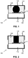
- FIG. 1 schematically depicts a first embodiment of a discrete semiconductor device package 100 of the present invention.
- a semiconductor die 110 e.g. a monocrystalline or polycrystalline silicon die, of a vertical semiconductor device, e.g. a vertical diode, carries a die contact 112, onto which a conductive body120 is formed, which in this embodiment is a solder or metal ball having a sufficiently high melting point, e.g. above 280°C.
- Such conductive bodies 120 may be formed in any suitable manner; for instance by depositing a solder, applying a gold or copper ball by e.g. wire bonding, applying a Ni contact in a plating bath, growing a copper pillar in a plating bath and so on.
- the conductive body may further comprise a solderable plating, e.g. a Sn plating or a plating having a sufficiently high melting point to improve solderability of the conductive body 120.
- the die contact 112 may be any suitable conductive material, e.g. a metal such as copper, aluminium, any suitable type of under-bump metallization and so on. To improve solderability, the die contact 112 may further be plated by a plating material selected from tin, silver, metal alloys, layer stacks such as Au provided with a Ni barrier layer (i.e. a NiAu finish), NiPdAu and so on. Any suitable conductive composition may be used for the formation of the conductive body120.
- the conductive body 120 is encapsulated in a molding material 130 such that the conductive body 120 makes conductive contact with a solder cap 140.
- the solder cap 140 may comprise any material that improves the adhesion of solder to the package 100.
- a plating material selected from tin, silver, metal alloys, layer stacks such as Au provided with a Ni barrier layer (i.e. a NiAu finish), NiPdAu and so on may be used.
- the molding material 130 typically is a polymer material, e.g. an epoxy resin. However, many other suitable molding polymer materials are known per se to the skilled person.
- the lateral dimensions of the conductive body 120 are smaller than the lateral dimensions of the semiconductor die 110, with the molding material 130 laterally extending from the conductive body 120 to the edge of the semiconductor die 110 such that the space from the die surface to the top of the conductive body120 in the discrete semiconductor device package 100 is completely filled with the molding material 130.
- the package 100 may further comprise a second solder cap 150 in conductive contact with a bottom contact (not shown) of the semiconductor die 110.
- solder caps to such packages is well-known per se, this will not be explained in further detail for the sake of brevity. It suffices to say that any suitable solder cap material may be used for the provision for the solder caps 140 and 150.
- the solder cap 150 may be the same or a different material as the solder cap 140. The same material is preferred for the sake of avoiding additional complexity in the packaging process.
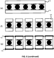
- FIG. 2 shows an alternative embodiment of the discrete semiconductor device package 100 of FIG. 1 , in which the conductive body 120 is replaced by a soldered or metal pillar 120. This demonstrates that the conductive body 120 in the discrete semiconductor device package 100 may have any suitable form.
- discrete semiconductor device packages are mounted on a carrier such as a PCB in a top/bottom contact orientation, with the bottom contact directly bonded to the carrier, and with the top contact being a wire bonding contact for wire bonding the top contact to the carrier.
- the provision of the wire bonding contact requires a minimum area which has prohibited the reduction of the package size beyond certain dimensions.
- the replacement of a wire bonding contact with the integrated conductive body120 in the discrete semiconductor device package 100 facilitates the sideways mounting of such packages on a carrier 200 such as a PCB as shown in FIG. 3 , with the solder caps 140 and 150 providing the contacts from the package 100 to the outside world.
- Carrier 200 has a first contact 210 and a second contact 220, to which the discrete semiconductor device package 100 is soldered using solder portions 250.
- the provision of the solder caps 140 and 150 on the end portions of the discrete semiconductor device package 100 enables the soldering 250 to extend vertically from the respective contacts 210 and 220.
- the sideways mounting of the discrete semiconductor device package 100 for instance allows the package to be used with PCBs that have been designed to receive larger form factor components, e.g. 0603 diode packages.
- a wafer 410 is provided that comprises a plurality of the semiconductor die portions 110, each carrying a die contact 112.
- the wafer 410 may be any suitable wafer, e.g. a monocrystalline or polycrystalline silicon wafer, a silicon-germanium wafer, a wafer comprising a heterojunction such as a wafer comprising gallium nitride heterojunction devices and so on.
- the die contacts 112 may be of any suitable conductive material, e.g. a metal. This preferably is a metal that is readily available in the applicable semiconductor process, e.g. copper for a silicon-based process.
- step (b) respective conductive bodies120, e.g. pillars or balls, are formed on each of the die contacts 112, after which the conductive bodies 120 are encapsulated in a molding material 130, e.g. a polymer or resin such as an epoxy resin or any other suitable polymer material, as shown in step (c). Excess molding material 130 may be removed in a planarization step (not shown) to expose the upper surfaces of the conductive bodies 120.
- a molding material 130 e.g. a polymer or resin such as an epoxy resin or any other suitable polymer material
- step (d) the wafer 410 is thinned to the desired thickness, e.g. by mechanical grinding and polishing followed by an optional back etch step or by a polishing step such as chemical mechanical polishing.
- the wafer 410 is subsequently singulated in step (e) to form the individual discrete semiconductor device packages 100, e.g. by means of dicing or plasma-etching, after each discrete semiconductor device package 100 is completed by forming a solder cap 140 over the surface comprising the exposed part of the conductive body 120 and forming a solder cap 150 over the exposed (bottom) surface of the semiconductor die 110 of the discrete semiconductor device package 100.
- the molding material 130 is formed on top of the surface of the semiconductor die 110 that carries the contact 112, such that the conductive body120 is (laterally) encapsulated by the molding material 130.
- the molding material 130 is made to extend over the sides of the semiconductor die 110 that connect the surface of the semiconductor die 110 that carries the contact 112 with the opposite surface (i.e. the bottom surface) of the semiconductor die 110, such that the molding material 130 also encapsulates the semiconductor die 110, which has the advantage of added protection for the discrete semiconductor device package 100.
- FIG. 5 An embodiment of a method of manufacturing such discrete semiconductor device packages 100 is shown in FIG. 5 .
- Steps (a) and (b) are identical to steps (a) and (b) of the method shown in FIG. 4 and described above, such that these steps will not be described in detail again for the sake of brevity only.
- the wafer 410 is placed on a sawing tape or foil or some other mounting aid 510, but it should be understood that such a mounting aid may also be used in the method shown in FIG. 4 .
- step (c) the wafer 410 is partially diced to create trenches 520 in between the individual semiconductor devices, e.g. by a plasma etching or sawing step, with at least the mounting aid 510 keeping the individual semiconductor devices together.
- the width of the trenches 520 may be increased, i.e. the individual semiconductor devices may be spaced further apart from each other by stretching the mounting aid 510.
- a sawing blade having a relatively large thickness may be used to obtain the desired width for the trenches 520.
- step (d) the resultant structure is encapsulated in the molding material 130 as shown in step (d). It is noted that the trenches 520 are also filled with the molding material 130 in this step, thus providing encapsulation at the sides of the respective semiconductor dies 110.
- a planarizing step such as a chemical mechanical polishing step may be applied to the molding material 130 to expose the upper surfaces of the conductive bodies 120.
- a wafer thinning step may be applied as previously explained, followed by the singulation step (f) to form the individual discrete semiconductor device packages 100, e.g. by means of dicing (sawing) or plasma-etching.
- step (c) is performed by a dicing step using a sawing blade of a first thickness and the singulation step (f) is performed by a dicing step using a sawing blade of a second thickness that is smaller than the first thickness, such that the sawing blade of a second thickness can follow the trenches 520 filled with the molding material 130 without completely removing the molding material 130 from these trenches.
- each discrete semiconductor device package 100 is completed as shown in step (g) by forming a solder cap 140 over the surface comprising the exposed part of the conductive body120 and forming a solder cap 150 over the exposed (bottom) surface of the semiconductor die 110 of the discrete semiconductor device package 100.
- FIG.6 A further embodiment of a method of the present invention is shown in FIG.6 .
- Steps (a) and (b) are substantially identical to steps (a) and (b) of the method shown in FIG. 4 and described above, such that these steps will not be described in detail again for the sake of brevity only.
- the conductive body 120 is a bump or ball rather than a pillar as shown in FIG. 4 .
- a further semiconductor wafer 610 is provided consisting of a plurality of further die portions, each carrying a die contact 112'.
- the further die portions may define a separate semiconductor device, e.g.
- the die contacts 112' are conductively connected, e.g. soldered, to the conductive body 120 as shown in step (c), such that the further semiconductor dies can be seen as a capping member of the conductive body 120.
- the main advantage of a two-sided wafer-based packaging process is that it reduces manufacturing complexity and therefore the cost of the resulting discrete semiconductor device package 100.
- the further semiconductor wafer 610 may be divided into smaller portions prior to soldering the die contacts 112' of such a wafer partition to the conductive bodies 120. This may be necessary in order to obtain the required alignment accuracy in the placement of the further semiconductor die 610 on the solder portions 120.
- step (d) the conductive bodies 120 are encapsulated in the encapsulation or molding material 130 as previously explained, after which an optional thinning step of the wafer 410 and/or the further wafer 610 may be performed as previously explained This is shown in step (e).
- step (f) the individual discrete semiconductor device packages 100 are formed by a singulation step, e.g. a dicing (sawing) or plasma-etching step, after which the solder caps 140 and 150 are formed over the respective bottom surfaces of the semiconductor dies in each package as shown in step (g).
- a singulation step e.g. a dicing (sawing) or plasma-etching step
- step (g) may be omitted in an alternative embodiment, i.e. each package may be provided without solder caps, in which case the bottom surfaces of the semiconductor dies act as the caps of the package as previously explained.
- the wafers 110 and 610 comprise a solderable back metal stack onto which the carrier solder can be directly applied.
Landscapes
- Structures Or Materials For Encapsulating Or Coating Semiconductor Devices Or Solid State Devices (AREA)
- Engineering & Computer Science (AREA)
- Manufacturing & Machinery (AREA)
- Led Device Packages (AREA)
Claims (12)
- Boîtier de composant semi-conducteur discret (100) comprenant :une puce semi-conductrice (110, 410) présentant une première surface et une seconde surface opposée à ladite première surface, ladite seconde surface portant un contact (112) ;un corps conducteur (120) sur ledit contact, dans lequel le corps conducteur (120) a une dimension latérale inférieure à la dimension latérale de la puce semi-conductrice (110, 410) ;un matériau d'encapsulation (130) formé par-dessus la seconde surface pour encapsuler latéralement ledit corps conducteur (120) ;un élément de surfaçage (140, 610) en contact conducteur avec le corps conducteur, ledit élément de surfaçage s'étendant par-dessus le matériau d'encapsulation, dans lequel l'élément de surfaçage (140, 610) comprend une autre puce semi-conductrice (610) et une couche de soudure (140), la couche de soudure (140) sur l'autre puce semi-conductrice (610), et une autre couche de soudure (150) en contact conducteur avec la première surface.
- Boîtier de composant semi-conducteur discret (100) selon l'une quelconque des revendications précédentes, dans lequel le corps conducteur (120) a une forme de bille ou de pilier.
- Boîtier de composant semi-conducteur discret (100) selon l'une quelconque des revendications précédentes, dans lequel le matériau d'encapsulation (130) s'étend également le long des côtés respectifs de la puce semi-conductrice (110) qui connectent la première surface à la seconde surface.
- Support (200) comprenant un premier contact de support (210) et un second contact de support (220), ledit support comprenant en outre le boîtier de composant semi-conducteur discret (100) selon l'une quelconque des revendications 1 à 3, dans lequel le premier contact de support est connecté conductivement à la première surface et le second contact de support est connecté conductivement au corps conducteur (120) par des parties de soudure respectives (250).
- Procédé de fabrication d'un boîtier semi-conducteur discret (100), comprenant :la fourniture d'une tranche (410) comprenant une pluralité de composants semi-conducteurs discrets, chacun desdits composants semi-conducteurs discrets présentant une première surface et une seconde surface opposée à ladite première surface, ladite deuxième surface portant un contact (112) ;la formation de corps conducteurs respectifs (120) sur chacun desdits contacts ;l'encapsulation latérale des corps conducteurs en recouvrant au moins la surface de la tranche portant les corps conducteurs avec un matériau d'encapsulation (130) ;la séparation des composants semi-conducteurs discrets, dans lequel les corps conducteurs (120) ont une dimension latérale inférieure à la dimension latérale des composants semi-conducteurs discrets séparés ;la fourniture d'un élément de surfaçage (140, 610) par-dessus au moins le corps conducteur de chacun des composants semi-conducteurs discrets, dans lequel l'élément de surfaçage comprend une autre puce semi-conductrice (610) et une soudure (140) ;la fourniture d'une couche de soudure (140) sur l'autre puce semi-conductrice (610) ;etla fourniture d'une autre couche de soudure (150) en contact conducteur avec la première surface.
- Procédé selon la revendication 5, comprenant en outre l'amincissement de la surface de la tranche (410) comportant les premières surfaces respectives des composants semi-conducteurs discrets avant ladite étape des séparation.
- Procédé selon la revendication 5 ou 6, dans lequel l'étape de fourniture d'un élément de surfaçage (140) comprend la fourniture d'une couche de soudure sur chaque composant semi-conducteur discret séparé, le procédé comprenant en outre la fourniture d'une autre couche de soudure (150) par-dessus la première surface de chacun des composants semi-conducteurs discrets.
- Procédé selon l'une quelconque des revendications 5 à 7, dans lequel ladite étape de séparation comprend le découpage en dés ou la gravure au plasma de la tranche (410) pour fournir les composants semi-conducteurs discrets.
- Procédé selon l'une quelconque des revendications 5 à 8, comprenant en outre :la séparation partielle des composants semi-conducteurs discrets avant ladite étape de recouvrement, exposant ainsi les côtés de chaque composant semi-conducteur discret qui connectent la première surface à la seconde surface ; etdans lequel ladite étape de recouvrement comprend en outre le recouvrement desdits côtés avec le matériau d'encapsulation (130).
- Procédé selon la revendication 9, comprenant en outre :la pose de la tranche (410) sur une feuille métallique de scie (510) avant ladite étape de séparation partielle ; etl'étirement de la feuille métallique de scie après ladite étape de séparation partielle pour exposer les côtés respectifs des composants semi-conducteurs discrets.
- Procédé selon la revendication 9, dans lequel l'étape de séparation partielle comprend le sciage de la tranche (410) avec une lame de scie ayant une première épaisseur, et dans lequel ladite étape de séparation comprend le sciage de la tranche encapsulée avec une lame de scie ayant une seconde épaisseur inférieure à la première épaisseur.
- Procédé selon l'une quelconque des revendications 5 à 11, dans lequel l'étape de fourniture dudit élément de surfaçage (610) comprend en outre la fourniture d'une autre tranche semi-conductrice (610) sur lesdits corps conducteurs respectifs (120).
Priority Applications (4)
| Application Number | Priority Date | Filing Date | Title |
|---|---|---|---|
| EP12170528.9A EP2669936B1 (fr) | 2012-06-01 | 2012-06-01 | Ensemble de dispositif semi-conducteur discret et procédé de fabrication |
| US13/890,055 US8981566B2 (en) | 2012-06-01 | 2013-05-08 | Discrete semiconductor device package and manufacturing method |
| CN201310205500.4A CN103456706B (zh) | 2012-06-01 | 2013-05-29 | 分立半导体器件封装和制造方法 |
| US14/607,587 US9263335B2 (en) | 2012-06-01 | 2015-01-28 | Discrete semiconductor device package and manufacturing method |
Applications Claiming Priority (1)
| Application Number | Priority Date | Filing Date | Title |
|---|---|---|---|
| EP12170528.9A EP2669936B1 (fr) | 2012-06-01 | 2012-06-01 | Ensemble de dispositif semi-conducteur discret et procédé de fabrication |
Publications (2)
| Publication Number | Publication Date |
|---|---|
| EP2669936A1 EP2669936A1 (fr) | 2013-12-04 |
| EP2669936B1 true EP2669936B1 (fr) | 2018-02-14 |
Family
ID=46197104
Family Applications (1)
| Application Number | Title | Priority Date | Filing Date |
|---|---|---|---|
| EP12170528.9A Active EP2669936B1 (fr) | 2012-06-01 | 2012-06-01 | Ensemble de dispositif semi-conducteur discret et procédé de fabrication |
Country Status (3)
| Country | Link |
|---|---|
| US (2) | US8981566B2 (fr) |
| EP (1) | EP2669936B1 (fr) |
| CN (1) | CN103456706B (fr) |
Families Citing this family (5)
| Publication number | Priority date | Publication date | Assignee | Title |
|---|---|---|---|---|
| EP2453476A1 (fr) * | 2010-11-12 | 2012-05-16 | Nxp B.V. | Procédé d'emballage de dispositif semi-conducteur et emballage de dispositif semi-conducteur |
| EP3065172B1 (fr) | 2015-03-06 | 2024-12-04 | Nexperia B.V. | Dispositif semi-conducteur |
| US9741617B2 (en) | 2015-11-16 | 2017-08-22 | Amkor Technology, Inc. | Encapsulated semiconductor package and method of manufacturing thereof |
| JP6562150B2 (ja) * | 2016-04-05 | 2019-08-21 | 株式会社Ihi | 過給機 |
| US10256168B2 (en) | 2016-06-12 | 2019-04-09 | Nexperia B.V. | Semiconductor device and lead frame therefor |
Family Cites Families (13)
| Publication number | Priority date | Publication date | Assignee | Title |
|---|---|---|---|---|
| EP1025587A4 (fr) * | 1997-07-21 | 2000-10-04 | Aguila Technologies Inc | Boitier de puce de semiconducteur a bosses et son procede de fabrication |
| JP3923258B2 (ja) * | 2001-01-17 | 2007-05-30 | 松下電器産業株式会社 | 電力制御系電子回路装置及びその製造方法 |
| US20020109201A1 (en) * | 2001-02-09 | 2002-08-15 | Chein-Chang Chen | Rectifying device and method of fabrication thereof |
| US20050029666A1 (en) * | 2001-08-31 | 2005-02-10 | Yasutoshi Kurihara | Semiconductor device structural body and electronic device |
| DE102004030042B4 (de) | 2004-06-22 | 2009-04-02 | Infineon Technologies Ag | Halbleiterbauelement mit einem auf einem Träger montierten Halbleiterchip, bei dem die vom Halbleiterchip auf den Träger übertragene Wärme begrenzt ist, sowie Verfahren zur Herstellung eines Halbleiterbauelementes |
| US7235877B2 (en) * | 2004-09-23 | 2007-06-26 | International Rectifier Corporation | Redistributed solder pads using etched lead frame |
| US7656047B2 (en) * | 2005-01-05 | 2010-02-02 | Advanced Semiconductor Engineering, Inc. | Semiconductor device package and manufacturing method |
| JP4697228B2 (ja) * | 2005-04-18 | 2011-06-08 | 日立化成工業株式会社 | 電子装置の製造方法 |
| US8367471B2 (en) * | 2007-06-15 | 2013-02-05 | Micron Technology, Inc. | Semiconductor assemblies, stacked semiconductor devices, and methods of manufacturing semiconductor assemblies and stacked semiconductor devices |
| US20120032350A1 (en) * | 2010-08-06 | 2012-02-09 | Conexant Systems, Inc. | Systems and Methods for Heat Dissipation Using Thermal Conduits |
| EP2421032A1 (fr) | 2010-08-18 | 2012-02-22 | Nxp B.V. | Procédé d'emballage de dispositif semi-conducteur et emballage de dispositif semi-conducteur |
| EP2453474A1 (fr) | 2010-11-10 | 2012-05-16 | Nxp B.V. | Procédé d'emballage de dispositif semi-conducteur et emballage de dispositif semi-conducteur |
| EP2453476A1 (fr) | 2010-11-12 | 2012-05-16 | Nxp B.V. | Procédé d'emballage de dispositif semi-conducteur et emballage de dispositif semi-conducteur |
-
2012
- 2012-06-01 EP EP12170528.9A patent/EP2669936B1/fr active Active
-
2013
- 2013-05-08 US US13/890,055 patent/US8981566B2/en active Active
- 2013-05-29 CN CN201310205500.4A patent/CN103456706B/zh active Active
-
2015
- 2015-01-28 US US14/607,587 patent/US9263335B2/en active Active
Non-Patent Citations (1)
| Title |
|---|
| None * |
Also Published As
| Publication number | Publication date |
|---|---|
| US9263335B2 (en) | 2016-02-16 |
| US20150140739A1 (en) | 2015-05-21 |
| CN103456706B (zh) | 2016-12-28 |
| US20130320551A1 (en) | 2013-12-05 |
| EP2669936A1 (fr) | 2013-12-04 |
| US8981566B2 (en) | 2015-03-17 |
| CN103456706A (zh) | 2013-12-18 |
Similar Documents
| Publication | Publication Date | Title |
|---|---|---|
| KR102691710B1 (ko) | 반도체 디바이스 및 그 제조 방법 | |
| KR102205119B1 (ko) | 반도체 디바이스 및 그 제조 방법 | |
| KR102024472B1 (ko) | 반도체 디바이스 및 그 제조 방법 | |
| US8247269B1 (en) | Wafer level embedded and stacked die power system-in-package packages | |
| TWI631633B (zh) | 半導體裝置及在半導體晶粒周圍形成絕緣層的方法 | |
| US9716080B1 (en) | Thin fan-out multi-chip stacked package structure and manufacturing method thereof | |
| TWI557872B (zh) | 半導體裝置及用於形成具有垂直互連之薄剖面wlcsp於封裝覆蓋區的方法 | |
| TWI677034B (zh) | 單次式封裝 | |
| TWI557862B (zh) | 形成具有半導體晶粒的tsv插入物並在插入物的對置表面上形成增長式的互連結構之半導體元件及方法 | |
| US8383457B2 (en) | Semiconductor device and method of forming interposer frame over semiconductor die to provide vertical interconnect | |
| US9184139B2 (en) | Semiconductor device and method of reducing warpage using a silicon to encapsulant ratio | |
| US20210028150A1 (en) | Semiconductor device package and method for manufacturing the same | |
| TW201501227A (zh) | 在扇出晶圓級晶片尺寸封裝上堆疊半導體晶粒之半導體裝置和方法 | |
| US9263335B2 (en) | Discrete semiconductor device package and manufacturing method | |
| TW202115842A (zh) | 半導體裝置以及其製造方法 | |
| US20120286410A1 (en) | Semiconductor device packaging method and semiconductor device package | |
| TWI862968B (zh) | 具有用於散熱件和電磁干擾屏蔽件的分隔蓋的封裝件 | |
| CN108321128A (zh) | 封装结构及其制造方法 | |
| US9947632B2 (en) | Semiconductor device and method of making a semiconductor device | |
| KR20140042094A (ko) | 반도체 디바이스 및 그 제조 방법 | |
| TW202531402A (zh) | 半導體裝置及製造模製整合式被動裝置晶片堆疊晶圓的方法 | |
| TW202331861A (zh) | 半導體裝置和以開槽基板形成選擇性電磁干擾屏蔽的方法 |
Legal Events
| Date | Code | Title | Description |
|---|---|---|---|
| PUAI | Public reference made under article 153(3) epc to a published international application that has entered the european phase |
Free format text: ORIGINAL CODE: 0009012 |
|
| AK | Designated contracting states |
Kind code of ref document: A1 Designated state(s): AL AT BE BG CH CY CZ DE DK EE ES FI FR GB GR HR HU IE IS IT LI LT LU LV MC MK MT NL NO PL PT RO RS SE SI SK SM TR |
|
| AX | Request for extension of the european patent |
Extension state: BA ME |
|
| 17P | Request for examination filed |
Effective date: 20131031 |
|
| RBV | Designated contracting states (corrected) |
Designated state(s): AL AT BE BG CH CY CZ DE DK EE ES FI FR GB GR HR HU IE IS IT LI LT LU LV MC MK MT NL NO PL PT RO RS SE SI SK SM TR |
|
| 17Q | First examination report despatched |
Effective date: 20151130 |
|
| RAP1 | Party data changed (applicant data changed or rights of an application transferred) |
Owner name: NEXPERIA B.V. |
|
| RAP1 | Party data changed (applicant data changed or rights of an application transferred) |
Owner name: NEXPERIA B.V. |
|
| REG | Reference to a national code |
Ref country code: DE Ref legal event code: R079 Ref document number: 602012042743 Country of ref document: DE Free format text: PREVIOUS MAIN CLASS: H01L0021560000 Ipc: H01L0023310000 |
|
| GRAP | Despatch of communication of intention to grant a patent |
Free format text: ORIGINAL CODE: EPIDOSNIGR1 |
|
| RIC1 | Information provided on ipc code assigned before grant |
Ipc: H01L 23/00 20060101ALI20171026BHEP Ipc: H01L 21/56 20060101ALI20171026BHEP Ipc: H01L 23/31 20060101AFI20171026BHEP Ipc: H01L 25/00 20060101ALI20171026BHEP Ipc: H01L 25/065 20060101ALI20171026BHEP Ipc: H01L 21/78 20060101ALI20171026BHEP Ipc: H01L 23/485 20060101ALI20171026BHEP |
|
| INTG | Intention to grant announced |
Effective date: 20171127 |
|
| GRAS | Grant fee paid |
Free format text: ORIGINAL CODE: EPIDOSNIGR3 |
|
| GRAA | (expected) grant |
Free format text: ORIGINAL CODE: 0009210 |
|
| AK | Designated contracting states |
Kind code of ref document: B1 Designated state(s): AL AT BE BG CH CY CZ DE DK EE ES FI FR GB GR HR HU IE IS IT LI LT LU LV MC MK MT NL NO PL PT RO RS SE SI SK SM TR |
|
| REG | Reference to a national code |
Ref country code: GB Ref legal event code: FG4D |
|
| REG | Reference to a national code |
Ref country code: CH Ref legal event code: EP |
|
| REG | Reference to a national code |
Ref country code: IE Ref legal event code: FG4D |
|
| REG | Reference to a national code |
Ref country code: DE Ref legal event code: R096 Ref document number: 602012042743 Country of ref document: DE Ref country code: AT Ref legal event code: REF Ref document number: 970370 Country of ref document: AT Kind code of ref document: T Effective date: 20180315 |
|
| REG | Reference to a national code |
Ref country code: FR Ref legal event code: PLFP Year of fee payment: 7 |
|
| REG | Reference to a national code |
Ref country code: NL Ref legal event code: MP Effective date: 20180214 |
|
| REG | Reference to a national code |
Ref country code: AT Ref legal event code: MK05 Ref document number: 970370 Country of ref document: AT Kind code of ref document: T Effective date: 20180214 |
|
| PG25 | Lapsed in a contracting state [announced via postgrant information from national office to epo] |
Ref country code: HR Free format text: LAPSE BECAUSE OF FAILURE TO SUBMIT A TRANSLATION OF THE DESCRIPTION OR TO PAY THE FEE WITHIN THE PRESCRIBED TIME-LIMIT Effective date: 20180214 Ref country code: CY Free format text: LAPSE BECAUSE OF FAILURE TO SUBMIT A TRANSLATION OF THE DESCRIPTION OR TO PAY THE FEE WITHIN THE PRESCRIBED TIME-LIMIT Effective date: 20180214 Ref country code: LT Free format text: LAPSE BECAUSE OF FAILURE TO SUBMIT A TRANSLATION OF THE DESCRIPTION OR TO PAY THE FEE WITHIN THE PRESCRIBED TIME-LIMIT Effective date: 20180214 Ref country code: NL Free format text: LAPSE BECAUSE OF FAILURE TO SUBMIT A TRANSLATION OF THE DESCRIPTION OR TO PAY THE FEE WITHIN THE PRESCRIBED TIME-LIMIT Effective date: 20180214 Ref country code: NO Free format text: LAPSE BECAUSE OF FAILURE TO SUBMIT A TRANSLATION OF THE DESCRIPTION OR TO PAY THE FEE WITHIN THE PRESCRIBED TIME-LIMIT Effective date: 20180514 Ref country code: ES Free format text: LAPSE BECAUSE OF FAILURE TO SUBMIT A TRANSLATION OF THE DESCRIPTION OR TO PAY THE FEE WITHIN THE PRESCRIBED TIME-LIMIT Effective date: 20180214 Ref country code: FI Free format text: LAPSE BECAUSE OF FAILURE TO SUBMIT A TRANSLATION OF THE DESCRIPTION OR TO PAY THE FEE WITHIN THE PRESCRIBED TIME-LIMIT Effective date: 20180214 |
|
| PG25 | Lapsed in a contracting state [announced via postgrant information from national office to epo] |
Ref country code: AT Free format text: LAPSE BECAUSE OF FAILURE TO SUBMIT A TRANSLATION OF THE DESCRIPTION OR TO PAY THE FEE WITHIN THE PRESCRIBED TIME-LIMIT Effective date: 20180214 Ref country code: RS Free format text: LAPSE BECAUSE OF FAILURE TO SUBMIT A TRANSLATION OF THE DESCRIPTION OR TO PAY THE FEE WITHIN THE PRESCRIBED TIME-LIMIT Effective date: 20180214 Ref country code: LV Free format text: LAPSE BECAUSE OF FAILURE TO SUBMIT A TRANSLATION OF THE DESCRIPTION OR TO PAY THE FEE WITHIN THE PRESCRIBED TIME-LIMIT Effective date: 20180214 Ref country code: SE Free format text: LAPSE BECAUSE OF FAILURE TO SUBMIT A TRANSLATION OF THE DESCRIPTION OR TO PAY THE FEE WITHIN THE PRESCRIBED TIME-LIMIT Effective date: 20180214 Ref country code: GR Free format text: LAPSE BECAUSE OF FAILURE TO SUBMIT A TRANSLATION OF THE DESCRIPTION OR TO PAY THE FEE WITHIN THE PRESCRIBED TIME-LIMIT Effective date: 20180515 Ref country code: BG Free format text: LAPSE BECAUSE OF FAILURE TO SUBMIT A TRANSLATION OF THE DESCRIPTION OR TO PAY THE FEE WITHIN THE PRESCRIBED TIME-LIMIT Effective date: 20180514 |
|
| PGFP | Annual fee paid to national office [announced via postgrant information from national office to epo] |
Ref country code: FR Payment date: 20180613 Year of fee payment: 7 |
|
| PG25 | Lapsed in a contracting state [announced via postgrant information from national office to epo] |
Ref country code: AL Free format text: LAPSE BECAUSE OF FAILURE TO SUBMIT A TRANSLATION OF THE DESCRIPTION OR TO PAY THE FEE WITHIN THE PRESCRIBED TIME-LIMIT Effective date: 20180214 Ref country code: EE Free format text: LAPSE BECAUSE OF FAILURE TO SUBMIT A TRANSLATION OF THE DESCRIPTION OR TO PAY THE FEE WITHIN THE PRESCRIBED TIME-LIMIT Effective date: 20180214 Ref country code: PL Free format text: LAPSE BECAUSE OF FAILURE TO SUBMIT A TRANSLATION OF THE DESCRIPTION OR TO PAY THE FEE WITHIN THE PRESCRIBED TIME-LIMIT Effective date: 20180214 Ref country code: IT Free format text: LAPSE BECAUSE OF FAILURE TO SUBMIT A TRANSLATION OF THE DESCRIPTION OR TO PAY THE FEE WITHIN THE PRESCRIBED TIME-LIMIT Effective date: 20180214 Ref country code: RO Free format text: LAPSE BECAUSE OF FAILURE TO SUBMIT A TRANSLATION OF THE DESCRIPTION OR TO PAY THE FEE WITHIN THE PRESCRIBED TIME-LIMIT Effective date: 20180214 |
|
| PGFP | Annual fee paid to national office [announced via postgrant information from national office to epo] |
Ref country code: GB Payment date: 20180629 Year of fee payment: 7 |
|
| REG | Reference to a national code |
Ref country code: DE Ref legal event code: R097 Ref document number: 602012042743 Country of ref document: DE |
|
| PG25 | Lapsed in a contracting state [announced via postgrant information from national office to epo] |
Ref country code: SK Free format text: LAPSE BECAUSE OF FAILURE TO SUBMIT A TRANSLATION OF THE DESCRIPTION OR TO PAY THE FEE WITHIN THE PRESCRIBED TIME-LIMIT Effective date: 20180214 Ref country code: SM Free format text: LAPSE BECAUSE OF FAILURE TO SUBMIT A TRANSLATION OF THE DESCRIPTION OR TO PAY THE FEE WITHIN THE PRESCRIBED TIME-LIMIT Effective date: 20180214 Ref country code: CZ Free format text: LAPSE BECAUSE OF FAILURE TO SUBMIT A TRANSLATION OF THE DESCRIPTION OR TO PAY THE FEE WITHIN THE PRESCRIBED TIME-LIMIT Effective date: 20180214 Ref country code: DK Free format text: LAPSE BECAUSE OF FAILURE TO SUBMIT A TRANSLATION OF THE DESCRIPTION OR TO PAY THE FEE WITHIN THE PRESCRIBED TIME-LIMIT Effective date: 20180214 |
|
| PLBE | No opposition filed within time limit |
Free format text: ORIGINAL CODE: 0009261 |
|
| STAA | Information on the status of an ep patent application or granted ep patent |
Free format text: STATUS: NO OPPOSITION FILED WITHIN TIME LIMIT |
|
| 26N | No opposition filed |
Effective date: 20181115 |
|
| REG | Reference to a national code |
Ref country code: CH Ref legal event code: PL |
|
| PG25 | Lapsed in a contracting state [announced via postgrant information from national office to epo] |
Ref country code: SI Free format text: LAPSE BECAUSE OF FAILURE TO SUBMIT A TRANSLATION OF THE DESCRIPTION OR TO PAY THE FEE WITHIN THE PRESCRIBED TIME-LIMIT Effective date: 20180214 |
|
| REG | Reference to a national code |
Ref country code: BE Ref legal event code: MM Effective date: 20180630 |
|
| REG | Reference to a national code |
Ref country code: IE Ref legal event code: MM4A |
|
| PG25 | Lapsed in a contracting state [announced via postgrant information from national office to epo] |
Ref country code: MC Free format text: LAPSE BECAUSE OF FAILURE TO SUBMIT A TRANSLATION OF THE DESCRIPTION OR TO PAY THE FEE WITHIN THE PRESCRIBED TIME-LIMIT Effective date: 20180214 Ref country code: LU Free format text: LAPSE BECAUSE OF NON-PAYMENT OF DUE FEES Effective date: 20180601 |
|
| PG25 | Lapsed in a contracting state [announced via postgrant information from national office to epo] |
Ref country code: IE Free format text: LAPSE BECAUSE OF NON-PAYMENT OF DUE FEES Effective date: 20180601 Ref country code: CH Free format text: LAPSE BECAUSE OF NON-PAYMENT OF DUE FEES Effective date: 20180630 Ref country code: LI Free format text: LAPSE BECAUSE OF NON-PAYMENT OF DUE FEES Effective date: 20180630 |
|
| PG25 | Lapsed in a contracting state [announced via postgrant information from national office to epo] |
Ref country code: BE Free format text: LAPSE BECAUSE OF NON-PAYMENT OF DUE FEES Effective date: 20180630 |
|
| PG25 | Lapsed in a contracting state [announced via postgrant information from national office to epo] |
Ref country code: MT Free format text: LAPSE BECAUSE OF NON-PAYMENT OF DUE FEES Effective date: 20180601 |
|
| GBPC | Gb: european patent ceased through non-payment of renewal fee |
Effective date: 20190601 |
|
| PG25 | Lapsed in a contracting state [announced via postgrant information from national office to epo] |
Ref country code: TR Free format text: LAPSE BECAUSE OF FAILURE TO SUBMIT A TRANSLATION OF THE DESCRIPTION OR TO PAY THE FEE WITHIN THE PRESCRIBED TIME-LIMIT Effective date: 20180214 |
|
| PG25 | Lapsed in a contracting state [announced via postgrant information from national office to epo] |
Ref country code: GB Free format text: LAPSE BECAUSE OF NON-PAYMENT OF DUE FEES Effective date: 20190601 |
|
| PG25 | Lapsed in a contracting state [announced via postgrant information from national office to epo] |
Ref country code: HU Free format text: LAPSE BECAUSE OF FAILURE TO SUBMIT A TRANSLATION OF THE DESCRIPTION OR TO PAY THE FEE WITHIN THE PRESCRIBED TIME-LIMIT; INVALID AB INITIO Effective date: 20120601 Ref country code: PT Free format text: LAPSE BECAUSE OF FAILURE TO SUBMIT A TRANSLATION OF THE DESCRIPTION OR TO PAY THE FEE WITHIN THE PRESCRIBED TIME-LIMIT Effective date: 20180214 |
|
| PG25 | Lapsed in a contracting state [announced via postgrant information from national office to epo] |
Ref country code: FR Free format text: LAPSE BECAUSE OF NON-PAYMENT OF DUE FEES Effective date: 20190630 Ref country code: MK Free format text: LAPSE BECAUSE OF NON-PAYMENT OF DUE FEES Effective date: 20180214 |
|
| PG25 | Lapsed in a contracting state [announced via postgrant information from national office to epo] |
Ref country code: IS Free format text: LAPSE BECAUSE OF FAILURE TO SUBMIT A TRANSLATION OF THE DESCRIPTION OR TO PAY THE FEE WITHIN THE PRESCRIBED TIME-LIMIT Effective date: 20180614 |
|
| PGFP | Annual fee paid to national office [announced via postgrant information from national office to epo] |
Ref country code: DE Payment date: 20250626 Year of fee payment: 14 |
|
| REG | Reference to a national code |
Ref country code: DE Ref legal event code: R079 Ref document number: 602012042743 Country of ref document: DE Free format text: PREVIOUS MAIN CLASS: H01L0023310000 Ipc: H10W0074100000 |