EP2680319B1 - Procédé de fabrication d'un ensemble solaire - Google Patents
Procédé de fabrication d'un ensemble solaire Download PDFInfo
- Publication number
- EP2680319B1 EP2680319B1 EP13020021.5A EP13020021A EP2680319B1 EP 2680319 B1 EP2680319 B1 EP 2680319B1 EP 13020021 A EP13020021 A EP 13020021A EP 2680319 B1 EP2680319 B1 EP 2680319B1
- Authority
- EP
- European Patent Office
- Prior art keywords
- solar cell
- interconnection member
- terminal
- attached
- top surface
- Prior art date
- Legal status (The legal status is an assumption and is not a legal conclusion. Google has not performed a legal analysis and makes no representation as to the accuracy of the status listed.)
- Active
Links
Images





Classifications
-
- H—ELECTRICITY
- H10—SEMICONDUCTOR DEVICES; ELECTRIC SOLID-STATE DEVICES NOT OTHERWISE PROVIDED FOR
- H10F—INORGANIC SEMICONDUCTOR DEVICES SENSITIVE TO INFRARED RADIATION, LIGHT, ELECTROMAGNETIC RADIATION OF SHORTER WAVELENGTH OR CORPUSCULAR RADIATION
- H10F19/00—Integrated devices, or assemblies of multiple devices, comprising at least one photovoltaic cell covered by group H10F10/00, e.g. photovoltaic modules
- H10F19/90—Structures for connecting between photovoltaic cells, e.g. interconnections or insulating spacers
- H10F19/902—Structures for connecting between photovoltaic cells, e.g. interconnections or insulating spacers for series or parallel connection of photovoltaic cells
- H10F19/904—Structures for connecting between photovoltaic cells, e.g. interconnections or insulating spacers for series or parallel connection of photovoltaic cells characterised by the shapes of the structures
-
- B—PERFORMING OPERATIONS; TRANSPORTING
- B64—AIRCRAFT; AVIATION; COSMONAUTICS
- B64G—COSMONAUTICS; VEHICLES OR EQUIPMENT THEREFOR
- B64G1/00—Cosmonautic vehicles
- B64G1/22—Parts of, or equipment specially adapted for fitting in or to, cosmonautic vehicles
- B64G1/42—Arrangements or adaptations of power supply systems
- B64G1/44—Arrangements or adaptations of power supply systems using radiation, e.g. deployable solar arrays
- B64G1/443—Photovoltaic cell arrays
-
- H—ELECTRICITY
- H02—GENERATION; CONVERSION OR DISTRIBUTION OF ELECTRIC POWER
- H02S—GENERATION OF ELECTRIC POWER BY CONVERSION OF INFRARED RADIATION, VISIBLE LIGHT OR ULTRAVIOLET LIGHT, e.g. USING PHOTOVOLTAIC [PV] MODULES
- H02S30/00—Structural details of PV modules other than those related to light conversion
- H02S30/20—Collapsible or foldable PV modules
-
- H—ELECTRICITY
- H10—SEMICONDUCTOR DEVICES; ELECTRIC SOLID-STATE DEVICES NOT OTHERWISE PROVIDED FOR
- H10F—INORGANIC SEMICONDUCTOR DEVICES SENSITIVE TO INFRARED RADIATION, LIGHT, ELECTROMAGNETIC RADIATION OF SHORTER WAVELENGTH OR CORPUSCULAR RADIATION
- H10F19/00—Integrated devices, or assemblies of multiple devices, comprising at least one photovoltaic cell covered by group H10F10/00, e.g. photovoltaic modules
- H10F19/80—Encapsulations or containers for integrated devices, or assemblies of multiple devices, having photovoltaic cells
-
- H—ELECTRICITY
- H10—SEMICONDUCTOR DEVICES; ELECTRIC SOLID-STATE DEVICES NOT OTHERWISE PROVIDED FOR
- H10F—INORGANIC SEMICONDUCTOR DEVICES SENSITIVE TO INFRARED RADIATION, LIGHT, ELECTROMAGNETIC RADIATION OF SHORTER WAVELENGTH OR CORPUSCULAR RADIATION
- H10F19/00—Integrated devices, or assemblies of multiple devices, comprising at least one photovoltaic cell covered by group H10F10/00, e.g. photovoltaic modules
- H10F19/90—Structures for connecting between photovoltaic cells, e.g. interconnections or insulating spacers
- H10F19/902—Structures for connecting between photovoltaic cells, e.g. interconnections or insulating spacers for series or parallel connection of photovoltaic cells
- H10F19/906—Structures for connecting between photovoltaic cells, e.g. interconnections or insulating spacers for series or parallel connection of photovoltaic cells characterised by the materials of the structures
-
- H—ELECTRICITY
- H10—SEMICONDUCTOR DEVICES; ELECTRIC SOLID-STATE DEVICES NOT OTHERWISE PROVIDED FOR
- H10F—INORGANIC SEMICONDUCTOR DEVICES SENSITIVE TO INFRARED RADIATION, LIGHT, ELECTROMAGNETIC RADIATION OF SHORTER WAVELENGTH OR CORPUSCULAR RADIATION
- H10F77/00—Constructional details of devices covered by this subclass
- H10F77/80—Arrangements for preventing damage to photovoltaic cells caused by corpuscular radiation, e.g. for space applications
-
- H—ELECTRICITY
- H10—SEMICONDUCTOR DEVICES; ELECTRIC SOLID-STATE DEVICES NOT OTHERWISE PROVIDED FOR
- H10F—INORGANIC SEMICONDUCTOR DEVICES SENSITIVE TO INFRARED RADIATION, LIGHT, ELECTROMAGNETIC RADIATION OF SHORTER WAVELENGTH OR CORPUSCULAR RADIATION
- H10F77/00—Constructional details of devices covered by this subclass
- H10F77/93—Interconnections
- H10F77/933—Interconnections for devices having potential barriers
- H10F77/935—Interconnections for devices having potential barriers for photovoltaic devices or modules
-
- B—PERFORMING OPERATIONS; TRANSPORTING
- B64—AIRCRAFT; AVIATION; COSMONAUTICS
- B64G—COSMONAUTICS; VEHICLES OR EQUIPMENT THEREFOR
- B64G1/00—Cosmonautic vehicles
- B64G1/22—Parts of, or equipment specially adapted for fitting in or to, cosmonautic vehicles
- B64G1/52—Protection, safety or emergency devices; Survival aids
- B64G1/54—Protection against radiation
-
- Y—GENERAL TAGGING OF NEW TECHNOLOGICAL DEVELOPMENTS; GENERAL TAGGING OF CROSS-SECTIONAL TECHNOLOGIES SPANNING OVER SEVERAL SECTIONS OF THE IPC; TECHNICAL SUBJECTS COVERED BY FORMER USPC CROSS-REFERENCE ART COLLECTIONS [XRACs] AND DIGESTS
- Y02—TECHNOLOGIES OR APPLICATIONS FOR MITIGATION OR ADAPTATION AGAINST CLIMATE CHANGE
- Y02E—REDUCTION OF GREENHOUSE GAS [GHG] EMISSIONS, RELATED TO ENERGY GENERATION, TRANSMISSION OR DISTRIBUTION
- Y02E10/00—Energy generation through renewable energy sources
- Y02E10/50—Photovoltaic [PV] energy
Definitions
- the present invention relates to a method for manufacturing a solar cell assembly.
- solar cells have been widely used in various fields and applications.
- solar cell assembly and solar cell array which include one or more solar cells can be applied in communication devices, electric/electronic appliances, industrial facilities, and military and aerospace applications.
- an aerospace craft may have very limited area (for example, solar wings) to mount solar cells or solar cell array thereon.
- solar wings For example, density of solar cells would be a particularly important aspect for aerospace applications.
- the solar wings of aerospace craft generally are folded or curled/rolled when the aerospace craft is launched into the space by a rocket or a space shuttle, it is advantageous if the aspect ratio of the solar cell array can be reduced to minimum. In other words, it is desirable to reduce the height of the solar cell array.
- an aerospace craft on which the solar cell assembly or array is mounted, generally operates in an aerospace environment in which there is no air circumference to block the space particle rays (cosmic rays).
- a tip on the solar cell array may possibly cause electrical spark discharging in an aerospace environment, for example, due to the cosmic rays.
- Different approaches to electrically interconnecting solar cells and solar cell panels are described in US 3,375,141 A , JP 2003 318430 A , US 6,543725 B1 , US 7, 419, 377 B1 , GB 1,328,324 A and US 5, 180,440 A .
- a solar cell assembly comprises: a solar cell, and a conductive interconnection member, the interconnection member comprising a first portion and a second portion attached to the first portion with an angle formed therebetween, wherein the first portion is attached to a top surface of the solar cell, wherein at least an end portion of the second portion is capable of being bended together with at least an end portion of an second portion of an interconnection member of another said solar cell assembly, in an operating state.
- a solar cell array may comprise: a first solar cell assembly, comprising a first solar cell and a first conductive interconnection member, the first interconnection member comprising a first portion and a second portion attached to the first portion with an angle formed therebetween, wherein the first portion is attached to a top surface of the first solar cell, and a second solar cell assembly comprising a second solar cell and a second conductive interconnection member, the second interconnection member comprising a first portion and a second portion attached to the first portion with an angle formed therebetween, wherein the first portion of the second interconnection member is attached to a top surface of the second solar cell, wherein the first solar cell and the second solar cell are arranged adjacent to each other such that the second portion of the first interconnect member and the second portion of the second interconnection member are adjacent to each other, and wherein at least the end portion of the second portion of the first interconnection member is bended together with at least the end portion of the second portion of the second interconnection member.
- first and second interconnect members are attached to each other prior to being bended.
- first and second interconnection members are formed integrally with at least the end portions of the second portions thereof attached to each other.
- the solar cell array may further comprise a carrier, wherein the first and second solar cells are mounted onto the carrier with bottom surfaces of the first and second solar cells facing the carrier.
- a method for manufacturing a solar cell assembly comprises: providing a first solar cell assembly, the first solar cell assembly comprising a first solar cell and a first conductive interconnection member, the first interconnection member comprising a first portion and a second portion attached to the first portion with an angle formed therebetween, wherein the first portion is attached to a top surface of the first solar cell; providing a second solar cell assembly, the second solar cell assembly comprising a second solar cell and a second conductive interconnection member, the second interconnection member comprising a first portion and a second portion attached to the first portion with an angle formed therebetween, wherein the first portion of the second interconnection member is attached to a top surface of the second solar cell; arranging the first solar cell and the second solar cell adjacent to each other such that the second portion of the first interconnect member and the second portion of the second interconnection member are adjacent to each other; and bending at least the end portion of the second portion of the first interconnection member together with at least the end portion of the second portion of the second interconnection member
- a method for manufacturing a solar cell array may comprise: providing a first solar cell; attaching a first conductive interconnection member to the first solar cell with a first portion of the interconnection member attached to a top surface of the solar cell, the interconnection member comprising the first portion and a second portion attached to the first portion with an angle formed therebetween; providing a second solar cell; attaching a second conductive interconnection member to the second solar cell with a first portion of the second interconnection member attached to a top surface of the second solar cell, the second interconnection member comprising the first portion and a second portion attached to the first portion with an angle formed therebetween; arranging the first solar cell and the second solar cell adjacent to each other such that the second portion of the first interconnect member and the second portion of the second interconnection member are adjacent to each other; and bending at least the end portion of the second portion of the first interconnection member together with at least the end portion of the second portion of the second interconnection member.
- the method further comprises: attaching at least the end portions of the second portions of the first and second interconnect members to each other prior to said bending.
- the first and second interconnection members are formed integrally with at least the end portions of the second portions thereof attached to each other.
- Fig. 1 is a schematic perspective view of an example of a solar cell assembly 300, in which conductive interconnection members 106 through 109 are attached to a solar cell 100.
- Fig. 2 illustrates a sectional view taken along the line 2-2 of Fig. 1 .
- Fig. 3 is a schematic perspective view of an example of the solar cell 100.
- Fig. 4 illustrates a sectional view taken along the line 4-4 of Fig. 3 .
- the solar cell assembly 300 may include a solar cell 100 and a conductive interconnection member (106, 107, 108, or 109) attached to a top surface 101 of the solar cell 100, as illustrated in Fig. 1 .
- the solar cell 100 (hereinafter, also referred as first solar cell) may be cut out from a wafer in which wafer a number (for example, two, or, more or less) of solar cells are manufactured as those skilled in the art would apparently understand.
- An example of the solar cell 100 is illustrated In Fig. 3 .
- the solar cell 100 may include four (4) connection parts 102 through 105 (which can be referred as first connection parts hereinafter) formed on the top surface of the solar cell 100; however, the invention is not limited thereto as long as at least one connection part can be formed on the top surface 101 of the solar cell 100.
- connection parts 102-105 as shown are just exemplary and not for limiting the scope of the invention.
- the connection parts 102-105 can be flush with, or recessed from, the top surface 101, although they are illustrated as being projected from the top surface 101.
- pads formed on the top surface of the solar cell which can be surrounded by for example a passivation layer, can be used as the connection part.
- connection parts for example, various terminals formed on the top surface of the solar cell can also be used as appropriate.
- connection part is formed adjacent to an edge of the top surface of the solar cell.
- two of the connection parts 102 and 103 are formed adjacent to an edge 110 of the top surface 101 while other two connection parts 104 and 105 are formed adjacent to an opposite edge 111 of the top surface 101.
- the number and arrangement of the connection parts on the top surface of the solar cell should not be limited to those illustrated in the drawings.
- connection parts are illustrated as being aligned with the edge of the top surface of the solar cell in Fig. 4 , the invention should not be limited thereto.
- the outer edges of the connection parts may be slightly distanced from the edge of the top surface of the solar cell in an implementation of the embodiment.
- the interconnection members 106-109 can be attached to a top surface 101 of the solar cell 100 by, for example, welding or soldering.
- Each of the interconnection members 106-109 includes a first portion and a second portion attached to the first portion with an angle formed therebetween.
- the interconnection members 107 and 108 each include a first portion 1071/1081 and a second portion 1072/1082 attached to the first portion with an angle (which is not specifically indicated) formed therebetween.
- the angle formed by the first portion and the second portion of an interconnection member can be in a range from 85 degrees to 90 degrees.
- the first portion is substantially perpendicular to the second portion, as exemplary illustrated in Fig. 2 . That is, the interconnection member can be of an L-like shape in a sectional view.
- the interconnection members can be formed of metal, and for example, it can be a metal plate.
- molybdenum As material for forming the interconnection member, molybdenum; a nickel-cobalt ferrous alloy material designed to be compatible with the thermal expansion characteristics of borosilicate glass such as that available under the trade designation Kovar from Carpenter Technology Corporation; a nickel iron alloy material having a uniquely low coefficient of thermal expansion available under the trade designation Invar, FeNi36, or 64FeNi; or the like can be used.
- the first portion and the second portion of the interconnection member can be substantially rectangular in shape.
- the interconnection member, including the first and second portions may have a thickness in a range from about 0.0007 inches and 0.0013 inches (or between about 0.0178mm and 0.033mm).
- the interconnection member can be used for, among others, providing electric connection to/from the solar cell.
- the first portions of the interconnection members 106-109 can be attached to respective connection parts 102-105 of the solar cell 100.
- the interconnection member are attached to a respective connection part such that the second portion thereof is closer to the edge, which is adjacent thereto, than the first portion thereof, as illustrated In Figs. 1 and 2 .
- the bottom surface of the first portion of the interconnection member e.g., 106) Is located within the top surface of the respective connection part (e.g., 102) formed on the top surface of the solar cell 100, that is to say, not out of the circumference of the connection part.
- the first portion of the interconnection member (e.g., any of 106 through 109), which is to be attached to the respective connection part formed on the top surface of the solar cell 100, has a dimension (e.g., width) approximately equal to or less than that of the respective connection part.
- a dimension e.g., width
- connection parts formed on the top surface of the solar cell are not limited to the case as illustrated in Figs. 1-2 , accordingly, the number and arrangement of the interconnection members are also not limited to the case as illustrated in Figs. 3-4 .
- the correspondence between the connection parts and the interconnection members is not limited to a one-to-one manner, for example, there may possibly be such a case where two interconnection members are attached to a same connection part formed on the top surface of the solar cell; and vice versa.
- the interconnection member of another said solar cell assembly can be similar to the interconnection member as above described, and may comprise a first portion and the second portion attached to the first portion with an angle formed therebetween, and the first portion of the another interconnection member is attached to a connection part formed on a top surface of the another solar cell.
- Fig. 5 is a schematic sectional view of a solar cell assembly 500 according to another embodiment of the invention in which a glass cover 120 is disposed above the top surface 101 of the solar cell 100.
- the glass cover 120 is disposed above the top surface of the solar cell 100 to which the interconnection members (e.g. 107 and 108) have been attached. That is, the glass cover is disposed above the top surface of the solar cell 100 after the interconnection member (e.g. 107) is attached to the solar cell; and the invention should not be limited thereto. It is preferable that the glass cover is transparent for lights.
- the density of the solar cells, for example, in a solar cell array can be increased, that is, more solar cells can be mounted in a limited area, which would be advantageous.
- Fig. 6 is a schematic perspective view of another solar cell assembly 600 according to the embodiment of the invention.
- the solar cell assembly 600 according to this embodiment is substantially identical with that as illustrated in Fig. 1 , and may comprise: a solar cell 200 (hereinafter, referred as second solar cell), and interconnection members 206 through 209 each comprising a first portion and a second portion attached to the first portion with an angle formed therebetween, wherein the first portion of the second interconnection member is attached to a top surface 201 of the second solar cell.
- a solar cell 200 hereinafter, referred as second solar cell
- interconnection members 206 through 209 each comprising a first portion and a second portion attached to the first portion with an angle formed therebetween, wherein the first portion of the second interconnection member is attached to a top surface 201 of the second solar cell.
- the solar cell 200 can include connection parts (hereinafter, referred as second connection parts) 202 through 205 formed on the top surface 201 thereof and adjacent to edges of the top surface, respectively. And, the first portions of the second interconnection members 206-209 are attached to the respective connection parts 202-205 of the second solar cell.
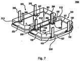
- Fig. 7 is a schematic perspective view of a solar cell array 700 according to a further embodiment, which comprises at least a first solar cell assembly (e.g., 500) and a second solar cell assembly (e.g., 600), in which the first solar cell and the second solar cell are arranged adjacent to each other.
- the first solar cell 100 and of the second solar cell 200 are arranged adjacent to each other such that second portions of the adjacent interconnection members for the first and second solar cells are adjacent to each other.
- the top surface 101 of the first solar cell 100 and the top surface 201 of the second solar cell 200 are arranged adjacent to each other, for example, laterally as illustrated in Fig.7 .
- edges 111 and 210 of the first and second solar cells which are respectively adjacent to the adjacent second portions are arranged such that a maximum distance between these two edges of the first and second solar cell is 0.15 inches or less, more preferably, no less than about 0.01 inches (or, about 0.254 mm) and no greater than about 0.15 inches (or, about 3.81 mm).
- Either or both of glass covers 120 and 220 can be disposed above the respective surface(s) 101 and/or 201 of the solar cell(s), after or prior to the arranging of the top surfaces 101 and 201.
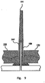
- Fig. 8 is a partially sectional view of the solar cell assembly taken along the line 7-7 in Fig. 7 , which illustrates the adjacent second portions 1082 and 2072 of the adjacent interconnection members 108 and 207.
- the second portions e.g., 1082 and 2072
- the present invention is not limited to the embodiment as shown in Fig. 8 .
- the length of a part of the second portion (e.g., 1082/2072) extending over a top surface of the corresponding glass cover may be in a range about from 0 to 0.1 inches (or, about 2.54 mm).
- the solar cells can be disposed or mounted very close to each other, thus the density of the solar cells in a unit area can be increased. Further, according to some certain embodiments, the aspect ratio of the solar cell array can be reduced, in other words, the height of the solar cell assembly and the solar cell array can be reduced. Moreover, the resistance capability against the strain or stress when the array is curled or stretched can be enhanced with use of the interconnection member according to the present disclosure.
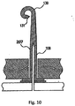
- Fig. 10 is a partially sectional view of the solar cell array, in which at least end portions of the adjacent second portions 1082 and 2072 of the adjacent interconnection members 108 and 207 as illustrated in Fig. 9 are bended together with each other. For example, they can be bended so that they can be curled or rolled into a spiral-like shape, as indicated by the reference number 130 in Fig. 10 ; and the present disclosure should not be limited thereto.
- the aspect ratio of the solar cell array can be further reduced, in other words, the height of the solar cell array can be further reduced. This is particularly advantageous in such a case where the solar cell array needs to be curled or rolled, for example, in the case where the aerospace craft, on which the solar cell array is mounted on its wings, is being launched by a rocket into the space. Further, because of the bending of the end portions, the resistance capability against the strain or stress due to, for example, the curling or stretching of the solar cell array can be further enhanced, thus the reliability of the solar cell array can be improved.
- the aerospace craft on which the solar cell array is mounted generally is operated in an aerospace environment in which there is no air circumference to block the space particle rays (cosmic rays).
- the tip 131 of the attached end portions of the second portions 1082 and 2072 may possibly cause sparkle discharging in an aerospace environment due to the cosmic rays.
- the sparkling discharge can be reduced or eliminated by reducing the length of the second portion extending over the top surface of the glass cover and/or bending the end portions.
- At least the end portions of the second portions 1082 and 2072 can be attached by welding, soldering, or the like, and then, the second portions 1082 and 2072 can be bended, for example, to be curled together, as illustrated in Figs. 9 and 10 .
- at least the end portions of the second portions 1082 and 2072 can be directly bended together with each other without the attaching process.
- the first and second interconnection members 108 and 207 can be integrally formed with at least the end portions of the second portions 1082 and 2072 thereof attached to each each other.
- the solar cell array may further comprise a carrier (not shown), wherein the solar cell(s), e.g., 100 and/or 200) can be mounted on the carrier by for example, silicone adhesive, with bottom surfaces thereof facing the carrier.
- the carrier can be formed of aluminium or titanium.
- the carrier is capable of being bended and stretched.
- Figs. 11 and 12 each illustrate a flow chart of an example of method for manufacturing a solar cell array according to an embodiment of the present disclosure.
- a method for manufacturing a solar cell array may comprises: providing (S1101) a first solar cell assembly, the first solar cell assembly comprising a first solar cell and a first interconnection member, the first interconnection member comprising a first portion and a second portion attached to the first portion with an angle formed therebetween, wherein the first portion is attached to a top surface of the first solar cell; providing (S1103) a second solar cell assembly, the second solar cell assembly comprising a second solar cell and a second interconnection member, the second interconnection member comprising a first portion and a second portion attached to the first portion with an angle formed therebetween, wherein the first portion of the second interconnection member is attached to a top surface of the second solar cell; arranging (S1105) the first solar cell and the second solar cell adjacent to each other such that the second portion of the first interconnect member and the second portion of the second interconnection member are adjacent to each other; and bending (S1107) at least the end portion of the second portion of the first interconnection member together with at least the
- a method for manufacturing a solar cell array may comprises: providing (S1201) a first solar cell; attaching (S1203) a first interconnection member to the first solar cell with a first portion of the interconnection member attached to a top surface of the solar cell, the interconnection member comprising the first portion and a second portion attached to the first portion with an angle formed therebetween; providing (S1205) a second solar cell; attaching (S1207) a second interconnection member to the second solar cell with a first portion of the second interconnection member attached to a top surface of the second solar cell, the second interconnection member comprising the first portion and a second portion attached to the first portion with an angle formed therebetween; arranging (S1209) the first solar cell and the second solar cell adjacent to each other such that the second portion of the first interconnect member and the second portion of the second interconnection member are adjacent to each other and bending (S1211) at least the end portion of the second portion of the first interconnection member together with at least the end portion of the second portion of the second inter
- the methods may further comprise: attaching at least the end portions of the second portions of the first and second interconnect members are attached to each other prior to said bending.
- the first and second interconnection members are formed integrally with at least the end portions of the second portions thereof attached to each other.
- said bending causes at least the end portions of the second portions of the first and second interconnection member to be curled into a spiral-like shape.
- At least one of the first and second interconnection members is a metal plate with L-like shape.
- At least one of the first and second interconnection members is formed of molybdenum; a nickel-cobalt ferrous alloy material designed to be compatible with the thermal expansion characteristics of borosilicate glass such as that available under the trade designation Kovar from Carpenter Technology Corporation; or a nickel iron alloy material having a uniquely low coefficient of thermal expansion available under the trade designation Invar, FeNi36, or 64FeNi.
- the first and second portions of at least one of the first and second interconnection members are substantially rectangular in shape, with a thickness in a range from about 0.0007 inches to about 0.0013 inches.
- the methods may further comprise: disposing a glass cover above the top surface of any one of the first and second solar cells after the corresponding interconnection member is attached to any one of the first and second solar cells.
- length of a part of the second portion of said any one of the first and second solar cells extending over a top surface of the glass cover is in a range from 0 to about 0.1 inches.
- each of the first and second solar cells further comprise a connection part formed on a top surface thereof and adjacent to an edge of the top surface, and wherein the first portions of the first and second interconnection members are attached to the respective connection parts of the first and second solar cell.
- said attaching of any of the first and second interconnection members is carried out by any of: welding or soldering.
- said arranging causes that a maximum distance between the respective edges of the first and second solar cells adjacent to the first and second interconnection members is 0.15 inches or less.
- the first solar cell includes at least two said first connection parts, one of the first connection parts for connection to a node of the first solar cell and another one of the first connection parts for connection to a cathode of the first solar cell.
- said attaching of a first interconnection member comprises: attaching at least two said first interconnection members to the respective first connection parts of the first solar cell.
- said attaching of at least one of the first and second interconnection members causes that the second portion of said at least one of the first and second interconnection members is closer to the corresponding edge, which is adjacent thereto, than the first portion thereof.
- the method may further comprise mounting the first and second solar cells onto the carrier with bottom surfaces of the first and second solar cells facing the carrier. Said mounting step can be performed after or before the interconnection member(s) for the first and/or the second solar cell is attached to the respective solar cell(s), depending on different implementations of the embodiment.
Landscapes
- Engineering & Computer Science (AREA)
- Life Sciences & Earth Sciences (AREA)
- Sustainable Development (AREA)
- Remote Sensing (AREA)
- Aviation & Aerospace Engineering (AREA)
- Photovoltaic Devices (AREA)
Claims (7)
- Un procédé de fabrication d'un réseau de cellules solaires (300) comprenant:fournir une première cellule solaire (100) ayant un premier terminal (104) disposé sur un côté de la première cellule solaire (100) adjacent à un premier bord (111) de la première cellule solaire (100), et un second terminal (103) disposé sur ledit un côté de la première cellule solaire (100) adjacent à un second bord de la première cellule solaire (100) opposé au premier bord (111);fournir une seconde cellule solaire (200) ayant un premier terminal (203) disposé sur un côté de la seconde cellule solaire (200) adjacent à un premier bord (211) de la seconde cellule solaire (200) et un second terminal disposé sur ledit un côté de la seconde cellule solaire (200) adjacent à un second bord de la seconde cellule solaire opposé au premier bord (211) de la seconde cellule solaire;fournir un premier élément d'interconnexion métallique (106-109) en forme de L, avec une première partie inférieure ayant une largeur approximativement égale ou inférieure à la largeur du premier terminal (104) de la première cellule solaire (100), et une seconde partie fixée à ladite première partie du premier élément d'interconnexion métallique (106-109) et s'étendant perpendiculairement à celle-ci; attacher de manière sûre la première partie inférieure du premier élément d'interconnexion métallique (106-109) au premier terminal (104) de la première cellule solaire (100);fournir un second élément d'interconnexion métallique (206-209) en forme de L, avec une première partie inférieure ayant une largeur approximativement égale ou inférieure à la largeur du second terminal de la seconde cellule solaire (200), et une seconde partie fixée à ladite première partie inférieure du second élément d'interconnexion métallique (206-209) et s'étendant perpendiculairement à celle-ci; attacher de manière sûre la première partie inférieure du second élément d'interconnexion métallique (206-209) au second terminal de la seconde cellule solaire (200);aligner le premier bord (111) de la première cellule solaire (100) avec le second bord de la seconde cellule solaire (200) de sorte que les deux bords soient sensiblement parallèles et espacés de manière uniforme d'au moins 0,0254 cm (0,01 pouce) et d'au plus 0,0381 cm (0,15 pouce) et la seconde partie du premier élément d'interconnexion métallique (106-109) soit adjacente à la seconde partie du second élément d'interconnexion métallique (206-209); etattacher de manière sûre la seconde partie du premier élément d'interconnexion métallique (106-109) à la seconde partie du second élément d'interconnexion métallique (206-209) de sorte qu'une interconnexion électriquement conductrice soit réalisée entre le premier terminal (104) de la première cellule solaire (100) et le second terminal de la seconde cellule solaire (200).
- Le procédé de fabrication d'un réseau de cellules solaires selon la revendication 1, comprenant en outre la fixation d'un verre de recouvrement sur la surface supérieure de la première cellule solaire et / ou dans lequel le verre de recouvrement est fixé à la première cellule solaire après le premier élément d'interconnexion métallique est attaché à la première cellule solaire.
- Le procédé de fabrication d'un réseau de cellules solaires selon la revendication 1, comprenant en outre le montage du côté inférieur des première et seconde cellules solaires sur un support.
- Le procédé de fabrication d'un réseau de cellules solaires selon la revendication 3, dans lequel le montage sur le support utilise un adhésif de silicone et / ou dans lequel le support est composé d'aluminium ou de titane.
- Le procédé de fabrication d'un réseau de cellules solaires selon la revendication 1, comprenant en outre l'étape consistant à plier la partie d'extrémité des secondes parties attachées des premier et second éléments d'interconnexion de sorte que la partie d'extrémité soit enroulée en une spirale.
- Le procédé de fabrication d'un réseau de cellules solaires selon la revendication 2, dans lequel la hauteur de la seconde partie du premier élément d'interconnexion sur la surface supérieure du verre de recouvrement peut être comprise entre 0,0 cm et 0,0254 cm (0,1 pouce).
- Le procédé de fabrication d'un réseau de cellules solaires selon la revendication 1, dans lequel le premier terminal correspond à un terminal d'anode de la cellule solaire et le second terminal correspond à un terminal de cathode de la cellule solaire.
Applications Claiming Priority (1)
| Application Number | Priority Date | Filing Date | Title |
|---|---|---|---|
| US13/535,570 US9102422B2 (en) | 2012-06-28 | 2012-06-28 | Solar cell assembly, solar cell panel, and method for manufacturing the same |
Publications (2)
| Publication Number | Publication Date |
|---|---|
| EP2680319A1 EP2680319A1 (fr) | 2014-01-01 |
| EP2680319B1 true EP2680319B1 (fr) | 2019-09-11 |
Family
ID=48470705
Family Applications (1)
| Application Number | Title | Priority Date | Filing Date |
|---|---|---|---|
| EP13020021.5A Active EP2680319B1 (fr) | 2012-06-28 | 2013-05-22 | Procédé de fabrication d'un ensemble solaire |
Country Status (3)
| Country | Link |
|---|---|
| US (2) | US9102422B2 (fr) |
| EP (1) | EP2680319B1 (fr) |
| DE (1) | DE102013008287B4 (fr) |
Families Citing this family (8)
| Publication number | Priority date | Publication date | Assignee | Title |
|---|---|---|---|---|
| US9117966B2 (en) | 2007-09-24 | 2015-08-25 | Solaero Technologies Corp. | Inverted metamorphic multijunction solar cell with two metamorphic layers and homojunction top cell |
| US9634172B1 (en) | 2007-09-24 | 2017-04-25 | Solaero Technologies Corp. | Inverted metamorphic multijunction solar cell with multiple metamorphic layers |
| US10381501B2 (en) | 2006-06-02 | 2019-08-13 | Solaero Technologies Corp. | Inverted metamorphic multijunction solar cell with multiple metamorphic layers |
| US10381505B2 (en) | 2007-09-24 | 2019-08-13 | Solaero Technologies Corp. | Inverted metamorphic multijunction solar cells including metamorphic layers |
| US9102422B2 (en) | 2012-06-28 | 2015-08-11 | Solaero Technologies Corp. | Solar cell assembly, solar cell panel, and method for manufacturing the same |
| TWI628909B (zh) | 2016-12-21 | 2018-07-01 | 財團法人工業技術研究院 | 具可擴充性的太陽能電池次模組 |
| USD845889S1 (en) | 2018-01-16 | 2019-04-16 | Solaero Technologies Corp. | Flexible interconnecting member for solar cells |
| US10529881B2 (en) | 2018-03-01 | 2020-01-07 | Solaero Technologies Corp. | Interconnect member |
Citations (4)
| Publication number | Priority date | Publication date | Assignee | Title |
|---|---|---|---|---|
| GB1328324A (en) * | 1971-03-19 | 1973-08-30 | Licentia Gmbh | Solar cell and method of producing solar cells |
| US5180442A (en) * | 1992-04-06 | 1993-01-19 | Eric Elias | Integration system for solar modules |
| US7419377B1 (en) * | 2007-08-20 | 2008-09-02 | Solaria Corporation | Electrical coupling device and method for solar cells |
| JP2008227085A (ja) * | 2007-03-12 | 2008-09-25 | Sharp Corp | 太陽電池アレイ、太陽電池モジュールおよび太陽電池アレイの製造方法 |
Family Cites Families (19)
| Publication number | Priority date | Publication date | Assignee | Title |
|---|---|---|---|---|
| US3375141A (en) | 1963-07-22 | 1968-03-26 | Aiken Ind Inc | Solar cell array |
| US5180689A (en) * | 1991-09-10 | 1993-01-19 | Taiwan Semiconductor Manufacturing Company | Tapered opening sidewall with multi-step etching process |
| DE19836272C2 (de) | 1998-08-11 | 2003-08-07 | Astrium Gmbh | Flexibler, faltbarer Solargenerator für Raumflugkörper |
| US6555739B2 (en) * | 2001-09-10 | 2003-04-29 | Ekla-Tek, Llc | Photovoltaic array and method of manufacturing same |
| JP3932029B2 (ja) | 2002-04-22 | 2007-06-20 | 富士電機ホールディングス株式会社 | 太陽電池モジュールの設置方法 |
| US7423346B2 (en) * | 2004-09-09 | 2008-09-09 | Megica Corporation | Post passivation interconnection process and structures |
| DE102004044061A1 (de) | 2004-09-11 | 2006-04-20 | Rwe Space Solar Power Gmbh | Solarzellenanordung sowie Verfahren zum Verschalten eines Solarzellenstrings |
| CN2818628Y (zh) | 2005-07-20 | 2006-09-20 | 常州天合光能有限公司 | 通用光伏建筑构件 |
| US7732705B2 (en) | 2005-10-11 | 2010-06-08 | Emcore Solar Power, Inc. | Reliable interconnection of solar cells including integral bypass diode |
| US7498508B2 (en) | 2006-02-24 | 2009-03-03 | Day4 Energy, Inc. | High voltage solar cell and solar cell module |
| US20100186804A1 (en) | 2009-01-29 | 2010-07-29 | Emcore Solar Power, Inc. | String Interconnection of Inverted Metamorphic Multijunction Solar Cells on Flexible Perforated Carriers |
| EP2132782B1 (fr) | 2007-02-15 | 2012-07-11 | Transform Solar Pty Ltd. | Assemblage de substrats, procédé d'assemblage et appareil d'assemblage |
| CN201038172Y (zh) | 2007-04-29 | 2008-03-19 | 厦门冠宇科技有限公司 | 柔性太阳能电池组件连接方式 |
| CN101483201A (zh) | 2008-02-26 | 2009-07-15 | 苏州斯派特光电技术有限公司 | 直连式薄膜太阳能电池模块及其制造方法 |
| US8263853B2 (en) | 2008-08-07 | 2012-09-11 | Emcore Solar Power, Inc. | Wafer level interconnection of inverted metamorphic multijunction solar cells |
| US7960201B2 (en) | 2009-01-29 | 2011-06-14 | Emcore Solar Power, Inc. | String interconnection and fabrication of inverted metamorphic multijunction solar cells |
| CN101853891B (zh) | 2009-04-02 | 2013-09-04 | 沙晓林 | 薄膜太阳能电池板阵列 |
| US20100282288A1 (en) | 2009-05-06 | 2010-11-11 | Emcore Solar Power, Inc. | Solar Cell Interconnection on a Flexible Substrate |
| US9102422B2 (en) | 2012-06-28 | 2015-08-11 | Solaero Technologies Corp. | Solar cell assembly, solar cell panel, and method for manufacturing the same |
-
2012
- 2012-06-28 US US13/535,570 patent/US9102422B2/en active Active
-
2013
- 2013-05-15 DE DE102013008287.0A patent/DE102013008287B4/de active Active
- 2013-05-22 EP EP13020021.5A patent/EP2680319B1/fr active Active
-
2015
- 2015-07-07 US US14/793,289 patent/US9153721B1/en active Active
Patent Citations (4)
| Publication number | Priority date | Publication date | Assignee | Title |
|---|---|---|---|---|
| GB1328324A (en) * | 1971-03-19 | 1973-08-30 | Licentia Gmbh | Solar cell and method of producing solar cells |
| US5180442A (en) * | 1992-04-06 | 1993-01-19 | Eric Elias | Integration system for solar modules |
| JP2008227085A (ja) * | 2007-03-12 | 2008-09-25 | Sharp Corp | 太陽電池アレイ、太陽電池モジュールおよび太陽電池アレイの製造方法 |
| US7419377B1 (en) * | 2007-08-20 | 2008-09-02 | Solaria Corporation | Electrical coupling device and method for solar cells |
Also Published As
| Publication number | Publication date |
|---|---|
| US20150311372A1 (en) | 2015-10-29 |
| EP2680319A1 (fr) | 2014-01-01 |
| DE102013008287A1 (de) | 2014-01-02 |
| DE102013008287B4 (de) | 2026-02-05 |
| US20140000672A1 (en) | 2014-01-02 |
| US9102422B2 (en) | 2015-08-11 |
| US9153721B1 (en) | 2015-10-06 |
Similar Documents
| Publication | Publication Date | Title |
|---|---|---|
| EP2680319B1 (fr) | Procédé de fabrication d'un ensemble solaire | |
| US9627565B2 (en) | Integral corner bypass diode interconnecting configuration for multiple solar cells | |
| CN109496366B (zh) | 电池到电池互连件 | |
| CN109273803A (zh) | 二次电池模块 | |
| EP2767840A1 (fr) | Montage de mesure pour batterie solaire et procédé de mesure de sortie de cellule de batterie solaire | |
| EP2894676B1 (fr) | Réseau de cellules solaires ayant deux types différents de cellules | |
| US9324896B2 (en) | Thermal receiver for high power solar concentrators and method of assembly | |
| CN103682227B (zh) | 用于电连接蓄电池模块的蓄电池单池的ω形的连接元件 | |
| CN110098275A (zh) | 太阳能电池互连件 | |
| JP2021529426A (ja) | 距離補償要素、距離補償要素としての金属箔の使用、および距離補償要素を備えた配置物 | |
| EP3648198A1 (fr) | Batterie rechargeable | |
| CN110277960A (zh) | 具有高封装密度的可卷曲太阳能电源模块 | |
| US20160190527A1 (en) | Battery module and manufacturing method thereof | |
| US9577131B2 (en) | Concentrator photovoltaic module, concentrator photovoltaic panel, and flexible printed circuit for concentrator photovoltaic module | |
| WO2007001004A1 (fr) | Cellule pour pile solaire | |
| US20240356170A1 (en) | Battery and electronic device | |
| CN202855777U (zh) | 太阳能电池组件及太阳能电池面板 | |
| US20220231184A1 (en) | Method for producing solar cells and solar cell assemblies | |
| JP2020123744A (ja) | 熱電発電機 | |
| CN103633167B (zh) | 太阳能电池组件、太阳能电池面板、及其制造方法 | |
| US10930835B2 (en) | Thermoelectric module sheet and thermoelectric module assembly including the same | |
| US12382729B2 (en) | Protection of space solar cells in an arrangement in the form of a string | |
| EP3282490A1 (fr) | Interconnecteur et panneau solaire | |
| US20250151419A1 (en) | Photovoltaic module assembly with optimised quantity of electrically conductive adhesive | |
| EP3428981A1 (fr) | Module de conversion thermoélectrique |
Legal Events
| Date | Code | Title | Description |
|---|---|---|---|
| PUAI | Public reference made under article 153(3) epc to a published international application that has entered the european phase |
Free format text: ORIGINAL CODE: 0009012 |
|
| AK | Designated contracting states |
Kind code of ref document: A1 Designated state(s): AL AT BE BG CH CY CZ DE DK EE ES FI FR GB GR HR HU IE IS IT LI LT LU LV MC MK MT NL NO PL PT RO RS SE SI SK SM TR |
|
| AX | Request for extension of the european patent |
Extension state: BA ME |
|
| 17P | Request for examination filed |
Effective date: 20140701 |
|
| RBV | Designated contracting states (corrected) |
Designated state(s): AL AT BE BG CH CY CZ DE DK EE ES FI FR GB GR HR HU IE IS IT LI LT LU LV MC MK MT NL NO PL PT RO RS SE SI SK SM TR |
|
| RAP1 | Party data changed (applicant data changed or rights of an application transferred) |
Owner name: SOLAERO TECHNOLOGIES CORP. |
|
| STAA | Information on the status of an ep patent application or granted ep patent |
Free format text: STATUS: EXAMINATION IS IN PROGRESS |
|
| 17Q | First examination report despatched |
Effective date: 20161209 |
|
| REG | Reference to a national code |
Ref country code: DE Ref legal event code: R079 Ref document number: 602013060251 Country of ref document: DE Free format text: PREVIOUS MAIN CLASS: H01L0031045000 Ipc: H01L0031050000 |
|
| GRAP | Despatch of communication of intention to grant a patent |
Free format text: ORIGINAL CODE: EPIDOSNIGR1 |
|
| STAA | Information on the status of an ep patent application or granted ep patent |
Free format text: STATUS: GRANT OF PATENT IS INTENDED |
|
| RIC1 | Information provided on ipc code assigned before grant |
Ipc: H02S 30/20 20140101ALI20190228BHEP Ipc: H01L 31/048 20140101ALI20190228BHEP Ipc: B64G 1/54 20060101ALI20190228BHEP Ipc: B64G 1/44 20060101ALI20190228BHEP Ipc: H01L 31/041 20140101ALI20190228BHEP Ipc: H01L 31/05 20140101AFI20190228BHEP |
|
| INTG | Intention to grant announced |
Effective date: 20190327 |
|
| GRAS | Grant fee paid |
Free format text: ORIGINAL CODE: EPIDOSNIGR3 |
|
| GRAA | (expected) grant |
Free format text: ORIGINAL CODE: 0009210 |
|
| STAA | Information on the status of an ep patent application or granted ep patent |
Free format text: STATUS: THE PATENT HAS BEEN GRANTED |
|
| AK | Designated contracting states |
Kind code of ref document: B1 Designated state(s): AL AT BE BG CH CY CZ DE DK EE ES FI FR GB GR HR HU IE IS IT LI LT LU LV MC MK MT NL NO PL PT RO RS SE SI SK SM TR |
|
| REG | Reference to a national code |
Ref country code: GB Ref legal event code: FG4D |
|
| REG | Reference to a national code |
Ref country code: CH Ref legal event code: EP |
|
| REG | Reference to a national code |
Ref country code: AT Ref legal event code: REF Ref document number: 1179600 Country of ref document: AT Kind code of ref document: T Effective date: 20190915 |
|
| REG | Reference to a national code |
Ref country code: DE Ref legal event code: R096 Ref document number: 602013060251 Country of ref document: DE |
|
| REG | Reference to a national code |
Ref country code: IE Ref legal event code: FG4D |
|
| REG | Reference to a national code |
Ref country code: NL Ref legal event code: FP |
|
| REG | Reference to a national code |
Ref country code: LT Ref legal event code: MG4D |
|
| PG25 | Lapsed in a contracting state [announced via postgrant information from national office to epo] |
Ref country code: LT Free format text: LAPSE BECAUSE OF FAILURE TO SUBMIT A TRANSLATION OF THE DESCRIPTION OR TO PAY THE FEE WITHIN THE PRESCRIBED TIME-LIMIT Effective date: 20190911 Ref country code: HR Free format text: LAPSE BECAUSE OF FAILURE TO SUBMIT A TRANSLATION OF THE DESCRIPTION OR TO PAY THE FEE WITHIN THE PRESCRIBED TIME-LIMIT Effective date: 20190911 Ref country code: FI Free format text: LAPSE BECAUSE OF FAILURE TO SUBMIT A TRANSLATION OF THE DESCRIPTION OR TO PAY THE FEE WITHIN THE PRESCRIBED TIME-LIMIT Effective date: 20190911 Ref country code: NO Free format text: LAPSE BECAUSE OF FAILURE TO SUBMIT A TRANSLATION OF THE DESCRIPTION OR TO PAY THE FEE WITHIN THE PRESCRIBED TIME-LIMIT Effective date: 20191211 Ref country code: BG Free format text: LAPSE BECAUSE OF FAILURE TO SUBMIT A TRANSLATION OF THE DESCRIPTION OR TO PAY THE FEE WITHIN THE PRESCRIBED TIME-LIMIT Effective date: 20191211 Ref country code: SE Free format text: LAPSE BECAUSE OF FAILURE TO SUBMIT A TRANSLATION OF THE DESCRIPTION OR TO PAY THE FEE WITHIN THE PRESCRIBED TIME-LIMIT Effective date: 20190911 |
|
| PG25 | Lapsed in a contracting state [announced via postgrant information from national office to epo] |
Ref country code: RS Free format text: LAPSE BECAUSE OF FAILURE TO SUBMIT A TRANSLATION OF THE DESCRIPTION OR TO PAY THE FEE WITHIN THE PRESCRIBED TIME-LIMIT Effective date: 20190911 Ref country code: GR Free format text: LAPSE BECAUSE OF FAILURE TO SUBMIT A TRANSLATION OF THE DESCRIPTION OR TO PAY THE FEE WITHIN THE PRESCRIBED TIME-LIMIT Effective date: 20191212 Ref country code: AL Free format text: LAPSE BECAUSE OF FAILURE TO SUBMIT A TRANSLATION OF THE DESCRIPTION OR TO PAY THE FEE WITHIN THE PRESCRIBED TIME-LIMIT Effective date: 20190911 Ref country code: LV Free format text: LAPSE BECAUSE OF FAILURE TO SUBMIT A TRANSLATION OF THE DESCRIPTION OR TO PAY THE FEE WITHIN THE PRESCRIBED TIME-LIMIT Effective date: 20190911 Ref country code: ES Free format text: LAPSE BECAUSE OF FAILURE TO SUBMIT A TRANSLATION OF THE DESCRIPTION OR TO PAY THE FEE WITHIN THE PRESCRIBED TIME-LIMIT Effective date: 20190911 |
|
| REG | Reference to a national code |
Ref country code: AT Ref legal event code: MK05 Ref document number: 1179600 Country of ref document: AT Kind code of ref document: T Effective date: 20190911 |
|
| PG25 | Lapsed in a contracting state [announced via postgrant information from national office to epo] |
Ref country code: AT Free format text: LAPSE BECAUSE OF FAILURE TO SUBMIT A TRANSLATION OF THE DESCRIPTION OR TO PAY THE FEE WITHIN THE PRESCRIBED TIME-LIMIT Effective date: 20190911 Ref country code: PL Free format text: LAPSE BECAUSE OF FAILURE TO SUBMIT A TRANSLATION OF THE DESCRIPTION OR TO PAY THE FEE WITHIN THE PRESCRIBED TIME-LIMIT Effective date: 20190911 Ref country code: EE Free format text: LAPSE BECAUSE OF FAILURE TO SUBMIT A TRANSLATION OF THE DESCRIPTION OR TO PAY THE FEE WITHIN THE PRESCRIBED TIME-LIMIT Effective date: 20190911 Ref country code: RO Free format text: LAPSE BECAUSE OF FAILURE TO SUBMIT A TRANSLATION OF THE DESCRIPTION OR TO PAY THE FEE WITHIN THE PRESCRIBED TIME-LIMIT Effective date: 20190911 Ref country code: PT Free format text: LAPSE BECAUSE OF FAILURE TO SUBMIT A TRANSLATION OF THE DESCRIPTION OR TO PAY THE FEE WITHIN THE PRESCRIBED TIME-LIMIT Effective date: 20200113 |
|
| PG25 | Lapsed in a contracting state [announced via postgrant information from national office to epo] |
Ref country code: SM Free format text: LAPSE BECAUSE OF FAILURE TO SUBMIT A TRANSLATION OF THE DESCRIPTION OR TO PAY THE FEE WITHIN THE PRESCRIBED TIME-LIMIT Effective date: 20190911 Ref country code: SK Free format text: LAPSE BECAUSE OF FAILURE TO SUBMIT A TRANSLATION OF THE DESCRIPTION OR TO PAY THE FEE WITHIN THE PRESCRIBED TIME-LIMIT Effective date: 20190911 Ref country code: IS Free format text: LAPSE BECAUSE OF FAILURE TO SUBMIT A TRANSLATION OF THE DESCRIPTION OR TO PAY THE FEE WITHIN THE PRESCRIBED TIME-LIMIT Effective date: 20200224 Ref country code: CZ Free format text: LAPSE BECAUSE OF FAILURE TO SUBMIT A TRANSLATION OF THE DESCRIPTION OR TO PAY THE FEE WITHIN THE PRESCRIBED TIME-LIMIT Effective date: 20190911 |
|
| REG | Reference to a national code |
Ref country code: DE Ref legal event code: R097 Ref document number: 602013060251 Country of ref document: DE |
|
| PLBE | No opposition filed within time limit |
Free format text: ORIGINAL CODE: 0009261 |
|
| STAA | Information on the status of an ep patent application or granted ep patent |
Free format text: STATUS: NO OPPOSITION FILED WITHIN TIME LIMIT |
|
| PG2D | Information on lapse in contracting state deleted |
Ref country code: IS |
|
| PG25 | Lapsed in a contracting state [announced via postgrant information from national office to epo] |
Ref country code: DK Free format text: LAPSE BECAUSE OF FAILURE TO SUBMIT A TRANSLATION OF THE DESCRIPTION OR TO PAY THE FEE WITHIN THE PRESCRIBED TIME-LIMIT Effective date: 20190911 Ref country code: IS Free format text: LAPSE BECAUSE OF FAILURE TO SUBMIT A TRANSLATION OF THE DESCRIPTION OR TO PAY THE FEE WITHIN THE PRESCRIBED TIME-LIMIT Effective date: 20200112 |
|
| 26N | No opposition filed |
Effective date: 20200615 |
|
| PG25 | Lapsed in a contracting state [announced via postgrant information from national office to epo] |
Ref country code: SI Free format text: LAPSE BECAUSE OF FAILURE TO SUBMIT A TRANSLATION OF THE DESCRIPTION OR TO PAY THE FEE WITHIN THE PRESCRIBED TIME-LIMIT Effective date: 20190911 |
|
| REG | Reference to a national code |
Ref country code: DE Ref legal event code: R082 Ref document number: 602013060251 Country of ref document: DE Representative=s name: ADARES PATENT- UND RECHTSANWAELTE REININGER & , DE |
|
| PG25 | Lapsed in a contracting state [announced via postgrant information from national office to epo] |
Ref country code: MC Free format text: LAPSE BECAUSE OF FAILURE TO SUBMIT A TRANSLATION OF THE DESCRIPTION OR TO PAY THE FEE WITHIN THE PRESCRIBED TIME-LIMIT Effective date: 20190911 Ref country code: CH Free format text: LAPSE BECAUSE OF NON-PAYMENT OF DUE FEES Effective date: 20200531 Ref country code: LI Free format text: LAPSE BECAUSE OF NON-PAYMENT OF DUE FEES Effective date: 20200531 |
|
| PG25 | Lapsed in a contracting state [announced via postgrant information from national office to epo] |
Ref country code: LU Free format text: LAPSE BECAUSE OF NON-PAYMENT OF DUE FEES Effective date: 20200522 |
|
| PG25 | Lapsed in a contracting state [announced via postgrant information from national office to epo] |
Ref country code: IE Free format text: LAPSE BECAUSE OF NON-PAYMENT OF DUE FEES Effective date: 20200522 |
|
| PG25 | Lapsed in a contracting state [announced via postgrant information from national office to epo] |
Ref country code: TR Free format text: LAPSE BECAUSE OF FAILURE TO SUBMIT A TRANSLATION OF THE DESCRIPTION OR TO PAY THE FEE WITHIN THE PRESCRIBED TIME-LIMIT Effective date: 20190911 Ref country code: MT Free format text: LAPSE BECAUSE OF FAILURE TO SUBMIT A TRANSLATION OF THE DESCRIPTION OR TO PAY THE FEE WITHIN THE PRESCRIBED TIME-LIMIT Effective date: 20190911 Ref country code: CY Free format text: LAPSE BECAUSE OF FAILURE TO SUBMIT A TRANSLATION OF THE DESCRIPTION OR TO PAY THE FEE WITHIN THE PRESCRIBED TIME-LIMIT Effective date: 20190911 |
|
| PG25 | Lapsed in a contracting state [announced via postgrant information from national office to epo] |
Ref country code: MK Free format text: LAPSE BECAUSE OF FAILURE TO SUBMIT A TRANSLATION OF THE DESCRIPTION OR TO PAY THE FEE WITHIN THE PRESCRIBED TIME-LIMIT Effective date: 20190911 |
|
| PGFP | Annual fee paid to national office [announced via postgrant information from national office to epo] |
Ref country code: NL Payment date: 20220420 Year of fee payment: 10 |
|
| PGFP | Annual fee paid to national office [announced via postgrant information from national office to epo] |
Ref country code: IT Payment date: 20220412 Year of fee payment: 10 Ref country code: GB Payment date: 20220401 Year of fee payment: 10 Ref country code: FR Payment date: 20220408 Year of fee payment: 10 Ref country code: DE Payment date: 20220329 Year of fee payment: 10 |
|
| PGFP | Annual fee paid to national office [announced via postgrant information from national office to epo] |
Ref country code: BE Payment date: 20220420 Year of fee payment: 10 |
|
| REG | Reference to a national code |
Ref country code: DE Ref legal event code: R119 Ref document number: 602013060251 Country of ref document: DE |
|
| REG | Reference to a national code |
Ref country code: NL Ref legal event code: MM Effective date: 20230601 |
|
| GBPC | Gb: european patent ceased through non-payment of renewal fee |
Effective date: 20230522 |
|
| REG | Reference to a national code |
Ref country code: BE Ref legal event code: MM Effective date: 20230531 |
|
| PG25 | Lapsed in a contracting state [announced via postgrant information from national office to epo] |
Ref country code: NL Free format text: LAPSE BECAUSE OF NON-PAYMENT OF DUE FEES Effective date: 20230601 |
|
| PG25 | Lapsed in a contracting state [announced via postgrant information from national office to epo] |
Ref country code: IT Free format text: LAPSE BECAUSE OF NON-PAYMENT OF DUE FEES Effective date: 20230522 Ref country code: DE Free format text: LAPSE BECAUSE OF NON-PAYMENT OF DUE FEES Effective date: 20231201 Ref country code: GB Free format text: LAPSE BECAUSE OF NON-PAYMENT OF DUE FEES Effective date: 20230522 |
|
| PG25 | Lapsed in a contracting state [announced via postgrant information from national office to epo] |
Ref country code: FR Free format text: LAPSE BECAUSE OF NON-PAYMENT OF DUE FEES Effective date: 20230531 Ref country code: BE Free format text: LAPSE BECAUSE OF NON-PAYMENT OF DUE FEES Effective date: 20230531 |