EP2681768B1 - Verfahren zur monolitischen serienverschaltung von photovoltaischen zellen eines photovoltaikmoduls und dadurch hergestelltes photovoltaikmodul - Google Patents
Verfahren zur monolitischen serienverschaltung von photovoltaischen zellen eines photovoltaikmoduls und dadurch hergestelltes photovoltaikmodul Download PDFInfo
- Publication number
- EP2681768B1 EP2681768B1 EP12709930.7A EP12709930A EP2681768B1 EP 2681768 B1 EP2681768 B1 EP 2681768B1 EP 12709930 A EP12709930 A EP 12709930A EP 2681768 B1 EP2681768 B1 EP 2681768B1
- Authority
- EP
- European Patent Office
- Prior art keywords
- trench
- layer
- conductive layer
- conductive
- photovoltaic module
- Prior art date
- Legal status (The legal status is an assumption and is not a legal conclusion. Google has not performed a legal analysis and makes no representation as to the accuracy of the status listed.)
- Not-in-force
Links
Images



Classifications
-
- H—ELECTRICITY
- H10—SEMICONDUCTOR DEVICES; ELECTRIC SOLID-STATE DEVICES NOT OTHERWISE PROVIDED FOR
- H10F—INORGANIC SEMICONDUCTOR DEVICES SENSITIVE TO INFRARED RADIATION, LIGHT, ELECTROMAGNETIC RADIATION OF SHORTER WAVELENGTH OR CORPUSCULAR RADIATION
- H10F71/00—Manufacture or treatment of devices covered by this subclass
-
- H—ELECTRICITY
- H10—SEMICONDUCTOR DEVICES; ELECTRIC SOLID-STATE DEVICES NOT OTHERWISE PROVIDED FOR
- H10F—INORGANIC SEMICONDUCTOR DEVICES SENSITIVE TO INFRARED RADIATION, LIGHT, ELECTROMAGNETIC RADIATION OF SHORTER WAVELENGTH OR CORPUSCULAR RADIATION
- H10F19/00—Integrated devices, or assemblies of multiple devices, comprising at least one photovoltaic cell covered by group H10F10/00, e.g. photovoltaic modules
- H10F19/90—Structures for connecting between photovoltaic cells, e.g. interconnections or insulating spacers
- H10F19/902—Structures for connecting between photovoltaic cells, e.g. interconnections or insulating spacers for series or parallel connection of photovoltaic cells
-
- H—ELECTRICITY
- H10—SEMICONDUCTOR DEVICES; ELECTRIC SOLID-STATE DEVICES NOT OTHERWISE PROVIDED FOR
- H10F—INORGANIC SEMICONDUCTOR DEVICES SENSITIVE TO INFRARED RADIATION, LIGHT, ELECTROMAGNETIC RADIATION OF SHORTER WAVELENGTH OR CORPUSCULAR RADIATION
- H10F19/00—Integrated devices, or assemblies of multiple devices, comprising at least one photovoltaic cell covered by group H10F10/00, e.g. photovoltaic modules
-
- H—ELECTRICITY
- H10—SEMICONDUCTOR DEVICES; ELECTRIC SOLID-STATE DEVICES NOT OTHERWISE PROVIDED FOR
- H10F—INORGANIC SEMICONDUCTOR DEVICES SENSITIVE TO INFRARED RADIATION, LIGHT, ELECTROMAGNETIC RADIATION OF SHORTER WAVELENGTH OR CORPUSCULAR RADIATION
- H10F19/00—Integrated devices, or assemblies of multiple devices, comprising at least one photovoltaic cell covered by group H10F10/00, e.g. photovoltaic modules
- H10F19/30—Integrated devices, or assemblies of multiple devices, comprising at least one photovoltaic cell covered by group H10F10/00, e.g. photovoltaic modules comprising thin-film photovoltaic cells
- H10F19/31—Integrated devices, or assemblies of multiple devices, comprising at least one photovoltaic cell covered by group H10F10/00, e.g. photovoltaic modules comprising thin-film photovoltaic cells having multiple laterally adjacent thin-film photovoltaic cells deposited on the same substrate
- H10F19/33—Patterning processes to connect the photovoltaic cells, e.g. laser cutting of conductive or active layers
-
- H—ELECTRICITY
- H10—SEMICONDUCTOR DEVICES; ELECTRIC SOLID-STATE DEVICES NOT OTHERWISE PROVIDED FOR
- H10F—INORGANIC SEMICONDUCTOR DEVICES SENSITIVE TO INFRARED RADIATION, LIGHT, ELECTROMAGNETIC RADIATION OF SHORTER WAVELENGTH OR CORPUSCULAR RADIATION
- H10F19/00—Integrated devices, or assemblies of multiple devices, comprising at least one photovoltaic cell covered by group H10F10/00, e.g. photovoltaic modules
- H10F19/30—Integrated devices, or assemblies of multiple devices, comprising at least one photovoltaic cell covered by group H10F10/00, e.g. photovoltaic modules comprising thin-film photovoltaic cells
- H10F19/31—Integrated devices, or assemblies of multiple devices, comprising at least one photovoltaic cell covered by group H10F10/00, e.g. photovoltaic modules comprising thin-film photovoltaic cells having multiple laterally adjacent thin-film photovoltaic cells deposited on the same substrate
- H10F19/35—Structures for the connecting of adjacent photovoltaic cells, e.g. interconnections or insulating spacers
-
- Y—GENERAL TAGGING OF NEW TECHNOLOGICAL DEVELOPMENTS; GENERAL TAGGING OF CROSS-SECTIONAL TECHNOLOGIES SPANNING OVER SEVERAL SECTIONS OF THE IPC; TECHNICAL SUBJECTS COVERED BY FORMER USPC CROSS-REFERENCE ART COLLECTIONS [XRACs] AND DIGESTS
- Y02—TECHNOLOGIES OR APPLICATIONS FOR MITIGATION OR ADAPTATION AGAINST CLIMATE CHANGE
- Y02E—REDUCTION OF GREENHOUSE GAS [GHG] EMISSIONS, RELATED TO ENERGY GENERATION, TRANSMISSION OR DISTRIBUTION
- Y02E10/00—Energy generation through renewable energy sources
- Y02E10/50—Photovoltaic [PV] energy
-
- Y—GENERAL TAGGING OF NEW TECHNOLOGICAL DEVELOPMENTS; GENERAL TAGGING OF CROSS-SECTIONAL TECHNOLOGIES SPANNING OVER SEVERAL SECTIONS OF THE IPC; TECHNICAL SUBJECTS COVERED BY FORMER USPC CROSS-REFERENCE ART COLLECTIONS [XRACs] AND DIGESTS
- Y02—TECHNOLOGIES OR APPLICATIONS FOR MITIGATION OR ADAPTATION AGAINST CLIMATE CHANGE
- Y02E—REDUCTION OF GREENHOUSE GAS [GHG] EMISSIONS, RELATED TO ENERGY GENERATION, TRANSMISSION OR DISTRIBUTION
- Y02E10/00—Energy generation through renewable energy sources
- Y02E10/50—Photovoltaic [PV] energy
- Y02E10/541—CuInSe2 material PV cells
-
- Y—GENERAL TAGGING OF NEW TECHNOLOGICAL DEVELOPMENTS; GENERAL TAGGING OF CROSS-SECTIONAL TECHNOLOGIES SPANNING OVER SEVERAL SECTIONS OF THE IPC; TECHNICAL SUBJECTS COVERED BY FORMER USPC CROSS-REFERENCE ART COLLECTIONS [XRACs] AND DIGESTS
- Y02—TECHNOLOGIES OR APPLICATIONS FOR MITIGATION OR ADAPTATION AGAINST CLIMATE CHANGE
- Y02P—CLIMATE CHANGE MITIGATION TECHNOLOGIES IN THE PRODUCTION OR PROCESSING OF GOODS
- Y02P70/00—Climate change mitigation technologies in the production process for final industrial or consumer products
- Y02P70/50—Manufacturing or production processes characterised by the final manufactured product
Definitions
- the invention relates to the field of photovoltaic cells and more particularly to a method of manufacturing a monolithic series connection zone of photovoltaic cells.
- photovoltaic modules or “solar” modules, comprise one or more series arrangements of photovoltaic cells, each consisting of an absorption semiconducting zone interposed between a first conducting electrode and a second electrode.
- Light-transparent conductor constituting the face by which the cell is illuminated by solar radiation.
- the first electrode is commonly referred to as the "back” electrode and the second electrode is commonly referred to as the "forward" electrode.
- the photovoltaic cells are then individualized by forming trenches in the stack.
- the electrical series of two adjacent photovoltaic cells is preferably carried out by manufacturing a connection zone in the stack which defines both the individualization of the two cells and connects a front electrode of one of the cells with the back electrode of the other cell using only the constituent layers of the stack.
- This type of electrical connection called “monolithic”, has the advantage of not having to mechanically separate the cells and then carry them in a connection box making their serialization, and also avoids the use of wire and solder links . In addition, a gain in manufacturing cost and a gain in compactness are also obtained.
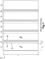
- the figure 1 is not to scale, the width of the monolithic connection areas 22, 24, 26, 28 having been exaggerated to make them more visible.
- the length L of photovoltaic cells 12, 14, 16, 18, 20 is usually between 1 millimeter and ten centimeters, said length L may even be greater than one meter, the width l of photovoltaic cells 12, 14, 16 , 18, 20 is usually of the order of a centimeter, while the width m of the monolithic connection zones 22, 24, 26, 28 is usually between 100 and 300 micrometers.
- the manufacturing method of the module 10 begins with the deposition of a conductive layer 30, usually a metal layer of a hard metal, preferably molybdenum, on an insulating substrate 32, usually made of glass, plastic or metal covered with a insulating layer.
- a conductive layer 30 usually a metal layer of a hard metal, preferably molybdenum, on an insulating substrate 32, usually made of glass, plastic or metal covered with a insulating layer.
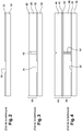
- an etching 34 is carried out in the metal layer 30 over the entire length thereof, for example by means of a UV or IR laser delivering pulses of a few picoseconds to a few nanoseconds ( figure 2 ).
- the semiconductor layer 36 is usually made in the form of a bilayer having a first lower layer 38 and a second upper layer 40.
- the lower layer 38 performs the absorption function of a predetermined electromagnetic radiation and is carried out in a polycrystalline alloy comprising at least copper, indium, galium and selenium, more commonly known as the "CIGS" alloy.
- the upper layer 40 forms a heterojunction with the lower semiconductor layer 38, and consists for example of a layer of cadmium sulphide (CdS) of a few tens of nanometers thick, for example 60 nanometers.
- CdS cadmium sulphide
- a first trench 42 is then etched in the stack thus produced, over the entire length L thereof, to the first metal layer 30 ( figure 3 ).
- a layer 44 conductive and transparent to light is then produced on the semiconductor layer 36.
- the layer 44 comprises for example an electrically conductive and transparent layer 48 of a hundred nanometers thick, for example 500 nanometers, especially ZnO doped with aluminum (ZnOAl) ( figure 3 ). Its function is improved by the presence of an optional layer 46, in particular a layer of zinc oxide (ZnO), very thin, typically a few tens of nanometers thick, for example 50 nanometers, rather resistive, which allows avoid forming short circuits with the semiconductor layer 36 when the surface state of the layer 38 is not very good.
- ZnO zinc oxide
- the constituent material of the upper layer 48 thus fills the trench 42 ( figure 4 ). It will be noted that the semiconductor layer 44 may also consist solely of the upper layer 48.
- the function of the layer 48 is however improved by the presence of the optional layer 46, which is very thin and relatively resistive, which makes it possible to avoid short circuits with the junction 36 when the surface condition of the lower semiconductor layer 38 is not of sufficient quality.
- the process is then continued by producing, for each monolithic connection zone 22, 24, 26, 28, a second trench 50, parallel to the first trench 42, in the thickness of the stack thus produced, over any the length L thereof and up to the metal layer 30.
- the layers 36 and 44 are friable and the metal layer 30 has a higher hardness than the layers 36, 44.
- the second trench 50 is usually made in a single step by lining the stack with a stylet ( figure 5 ).
- the etching 34 separates the rear electrodes 52, 54 of the cells 12 and 14, the electrical insulation between the two rear electrodes thus formed being formed by the semiconductor material of the absorbent layer 38 which separates them.
- the first and second trenches 42, 50 are made above the same rear electrode 54.
- the second trench 50 not adjacent to the etching 34, separates the front electrodes 56, 58 from the cells 12, 14, electrical insulation between the two front electrodes 56, 58 thus formed being formed by the medium 60 filling the second trench 50, usually air.
- the first trench 42 filled with the conductive material of the layer 48, has the function of defining an electrical path.
- the connection zone 22 defines an electrical path illustrated by the arrows of the figure 5 , electrically putting in series these cells, that is to say electrically connecting the front electrode 56 of the cell 12 with the rear electrode 54 of the cell 14.
- transversal refers to the direction of the stack, illustrated by the arrow X on the figure 5
- lateral refers to a direction perpendicular to the direction of the stack.
- the electrical insulation between the rear electrodes 52, 54 depends on the value of the total lateral electrical resistance R 1 of the region of the semiconductor material filling the etching 34, and more particularly on its relationship with the total transverse electrical resistance R L of the semiconductor layer 38.
- the electric current preferably flows along the path of lower electrical resistance, so it should be ensured that the lateral resistance R 1 is much greater than the transverse resistance R L.
- the width of the trench 34 needs to be very high.
- the polycrystalline CIGS has a linear electrical resistance much greater than its transverse electrical resistance linear due to the direction of growth of the crystals during the deposition of the layer 38, it is necessary to provide a trench 34 with a width of at least 100 micrometers.
- the width of the monolithic connection zone is largely dictated by the width of the etching 34. Thus, a significant area is lost for the absorption of photons.
- the width of the etching 34 guarantees a minimum electrical insulation between the rear electrodes of two adjacent photovoltaic cells, this electrical insulation remains however still too weak, so that leak currents are observed between two rear electrodes , which affects the overall performance of the solar module. This defect gets worse as the components are miniaturized.
- connection areas of the prior art allow a significant gain in cost, compactness and ease of connection, but intrinsically have limitations regarding the electrical insulation of the rear electrodes of photovoltaic cells.
- the document WO2009007375 illustrates state-of-the-art methods for interconnecting adjacent thin-film solar cells on an insulating substrate.
- the object of the present invention is to provide monolithic connection areas for photovoltaic module, and a method of manufacturing thereof, which significantly increase the electrical insulation between the rear electrodes of the photovoltaic cells constituting the module.
- liquid which has an ability to deform under the effect of its own weight and capillary phenomena.
- an ink composed of a volatile solvent with conductive particles, in particular metal particles, in suspension.
- opaque pastes such as silver inks or carbon-platinum inks
- transparent pastes such as indium-tin oxide inks, or "ITO" inks (for indium tin oxide )
- the rear electrodes of the adjacent photovoltaic cells are, according to the invention, separated, not by the semiconductor material of the absorption layer, but by a cavity filled with the gas bathing the module during its manufacture, namely usually air.
- air has a much higher electrical resistance than the electrical resistance of any semiconductor, including the lateral electrical resistance of polycrystalline semiconductor materials, such as polycrystalline CIGS alloys. It is thus obtained a significant gain of electrical insulation between the rear electrodes of adjacent photovoltaic cells.
- the method according to the invention in addition to its primary purpose of manufacturing a cavity filled with air between rear electrodes, also has the advantage of preserving the simplest possible stacking process, namely a simple successive formation of layers.
- the manufacturing method of the invention by this choice of the moment of embodiment of the cavity combined with the choice of a suitable conductive solution, is very simple to implement, and requires a very small number of 'steps.
- the thickness of the second conductive layer may also be involved in the choice of the preceding parameters.
- the formation of the connection zone comprises the formation of a third trench in the stack, adjacent only to the second trench and distinct from the latter, from the second conductive layer to the second trench. to the first conductive layer.
- This third trench makes it possible to separate and isolate the front electrodes of the photovoltaic cells.
- the width of the second trench is chosen so that the conductive solution is not in contact with the portion of the second semiconductor layer of the second cell.
- the separation and isolation of the front electrodes is achieved by a sufficient width of the second trench and the fact that the solution does not form a bridge between the opposite edges of the second trench.
- the widths of the first and second trenches are selected as a function of the viscosity of the conductive solution. It is indeed possible to obtain the desired result by parameterizing the viscosity of the solution and the width of the trenches.
- the method comprises a step of texturing the walls of the first trench by three-dimensional patterns.
- the method comprises a step of forming pads on a surface of the substrate released by the formation of the first trench, the height of the pads being substantially equal to that of the first trench.
- the minimum lateral distance without material in the first trench is selected as a function of the viscosity of the conductive solution.
- the method comprises forming a periodic three-dimensional pattern comprising solid portions and recessed portions on a first wall of the first trench, and forming the same periodic pattern on a second wall of the first trench, opposite to the first wall, the motif of the second wall being offset from the pattern of the first wall so as to face the solid parts of the pattern of the first wall with the recessed portions of the pattern of the second wall.
- the inner surface of the first trench coming into contact with the solution is increased, which limits the penetration thereof. It can thus be chosen for example a solution with a viscosity lower than the viscosity that would be necessary in the absence of texturing and / or pads. Similarly, it is possible to choose a larger first trench if the process and / or the application require it.
- the deposition of the conductive solution is performed by screen printing, heliography, flexography, inkjet or spray.
- the invention also relates to a photovoltaic module as defined in claim 12, comprising at least two photovoltaic cells each comprising a light absorbing semiconductor zone interposed between a rear conductive electrode and a front conductive electrode at least partially transparent to light, the cells being electrically connected in series by means of a monolithic connection zone comprising a trench separating the rear electrodes.
- This module is preferably manufactured according to the aforementioned method.
- the constituent layers of this stack are for example identical in size and made of the same materials as the layers of the photovoltaic module of the state of the art described in connection with the Figures 1 to 5 .
- the semiconductor layer 36 is a bilayer comprising a lower absorption layer 38 of a predetermined electromagnetic radiation and an upper junction layer 40.
- the second conductive layer 44 may be a bilayer consisting of a lower layer optional 46 and an upper layer 48, as in the state of the art previously described.
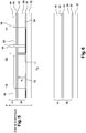
- the process continues by producing monolithic connection zones that individualize the photovoltaic cells while electrically connecting them in series.
- the first trench 70 is made for example by means of a laser etching in the thickness of the stack to the substrate 32.
- the second and third trenches 72, 74 are in turn made in the thickness of the stacking up to the conductive layer 30, for example by means of a stripe by a stylus or by laser or by chemical etching.
- the first trench 70 thus separates the layer 30 into two parts, forming respectively the rear electrodes 52, 54 of a first and a second adjacent photovoltaic cells 12, 14, the rear electrodes 52, 54 being isolated from one another. another through the trench 70, which forms a cavity filled with air.
- the third trench 74 not adjacent to the first trench 70, separates for its part the front electrodes 56, 58 of the cells 12, 14, the electrical insulation between the two rear electrodes 52, 54 being made by the air filling the third trench 74.
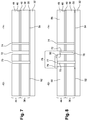
- a conductive solution 76 is then deposited on an area 78 of the second conductive layer 44, this area 78 comprising the first and the second trench 70, 72, this deposit being made for example by screen printing or by spraying.
- the solution 76 is transparent or semi-transparent and is for example a solution of indium oxide doped with tin (or "ITO"), a solution of ZnOAl, a solution of indium oxide doped with zinc ( or "IZO"), a solution of polymer with carbon nanotubes, or a polyme solution PEDOT (polyethylenedioxythiophene).
- the solution may be opaque, for example still platinum carbon (CPt) or silver ink.
- the solution 76 has the function of electrically connecting the front electrode 56 of the cell 12 with the rear electrode 54 of the cell 14. For this purpose, the solution 76 covers the first trench 70 and enters the second trench 72. filling the latter to a level sufficiently high to be in contact with the second conductive layer 44.
- the solution 76 does not penetrate in the first trench 70 and possibly form only a drop 77 inside the trench 70, or the solution 76 enters the first trench 70 but at a depth such that it does not reach the semiconductor layer of the trench 70 absorption 38.
- the conductive solution 76 is then solidified, for example by evaporation of a solvent if it is a solvent-based solution or by thermosetting if it is a thermosetting material.
- the photovoltaic cells 12 and 14 are thus connected electrically in series by the electrical path illustrated by the arrows of the figure 8 which connects the rear electrode 52 of the cell 12 with the front electrode of the cell 14.
- the figure 8 illustrates a variant in which the deposition of the solution 76 gave rise to a rupture 80 between firstly the solidified solution deposited on the trench 70 and secondly the solidified solution deposited in the second trench 72.
- the rupture zone 80 whose dimensions are here exaggerated, may for example occur due to a limited amount of solution deposited around the second trench 72 and / or the solidification process.
- the figure 9 illustrates a variant in which such a break is absent.
- the volume of solution deposited in the second trench 72 is greater than previously, so that the solution completely fills the second trench and forms, once frozen, a continuous zone.
- the electrical path differs from that of the figure 8 and includes only conductive materials.
- the separation of the front electrodes of two adjacent cells 12, 14 is implemented by means of the third trench 74.
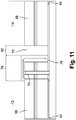
- a method of manufacturing a photovoltaic module according to a second embodiment of the invention is described in connection with the figures 10 and 11 .
- the individualization and the connection of two adjacent cells are made by means of only two trenches. More particularly, the process starts with the formation of the stack of layers 30, 32, 36, 44 as described in connection with the figure 6 , and continues with the formation of the first and second trenches 70 and 72 as described in connection with the figure 7 ( figure 10 ).
- a conductive solution 76 is then deposited on an area 78 of the second conductive layer 44 comprising the first and the second trench 70, 72, this deposit being made for example by ink jet, by sputtering or by screen printing.
- the conductive solution 76 and / or the width of the second trench 72 are chosen so that the solution 76 does not reach the edge of the second trench 72 corresponding to the second cell 14 ( figure 11 ). There is thus, in the second trench 72, a space 82 filled with air, which isolates the front electrodes 56, 58 from the adjacent cells 12, 14.
- the electrical path connecting the rear electrode 52 of the cell 12 with the electrode before 58 of the second cell is illustrated by the arrows.
- solution 76 forms a continuous zone but may, alternatively, have a rupture similar to that of the figure 8 .
- the non-penetration or the limited penetration of the solution 76 in the first trench 70 is obtained by parametering the width of the first trench, the viscosity of the deposited solution, the thickness of the second conductive layer 44, the accuracy of the method of deposit, and the volume deposited on the first trench 70.
- the absorption semiconductor layer 38 represents between a quarter and a third of the total height of the first trench 70. Ensuring that the solution 76 does not penetrate more than a quarter of the trench 70 avoids therefore any risk of short circuit because there will be no contact between the solution 76 and the semiconductor absorption layer 38, and therefore a fortiori with the conductive layer 30.
- a CPt ink with a viscosity of 3.2 cPoise, and therefore less than the limit of 50 cPoise maximum usually required for spraying, deposited by spraying to a thickness of 10 microns with an ultrasound frequency of 48 kHz , and a width of the first trench of less than 15 micrometers makes it possible to preserve the ink CPt on the surface with a weak penetration in the trench 70.
- the width of the trench once the other parameters of the deposit (viscosity of the solution, volume of solution deposited, thickness of the second conductive layer, type of deposit method used) determined.
- the penetration of the solution in the first trench by choosing the type of solidification of the solution. For example, by choosing a thermosetting solution, it is possible to stop the progression of this solution in the first trench by heating it. Similarly, by choosing a crosslinkable polymer solution, it is possible to stop its progression by subjecting it to appropriate radiation.
- first trench 70 whose edges are flat.
- the transverse walls thereof comprise, at least in the upper part of the trench 70, surface texturing so as to form three-dimensional patterns, as example shown on the top view of the figure 12A .
- each of the walls 90, 92 of the first trench 70 comprises a periodic array of patterns 94, 96 of rectangular section, the network 94 of a wall 90 being offset relative to the network 96 of the other wall 92 to that a pattern of a wall is arranged in front of a recessed portion of the other wall.
- the geometry of the patterns defined by the parameters L, 1, ⁇ , ⁇ illustrated in figure 12A , is also chosen so that the minimum lateral distance between any point of the first wall and any point of the second wall is less than the distance necessary to prevent the penetration of the solution in the trench 70, for example less than 15 micrometers in the previous example of the deposition of an ink CPt as previously described.
- the patterns thus make it possible, with an equal trench width, to increase the surface area in contact with the solution, and thus to be able to choose a less viscous solution if the application requires it, for example due to constraints on the deposition process or on the manufacture of the solution.
- Rectangular patterns have been described. However, as illustrated in Figures 12B to 12I , other patterns are possible on the walls of the first trench, the geometry of the patterns being chosen so as to obtain the minimum lateral distance which avoids or limits the penetration of the solution, between any point of the first wall and a point any of the second wall.
Landscapes
- Photovoltaic Devices (AREA)
Claims (16)
- Ein Verfahren zur Herstellung eines Photovoltaikmoduls, bestehend aus mindestens zwei nebeneinanderliegenden, in Reihe geschalteten photovoltaischen Zellen (12, 14) umfassend:▪ die Bildung eines isolierenden Substrats (32);▪ die Bildung eines Stapels, umfassend:∘ eine erste elektrisch leitfähige Schicht (30), die auf dem isolierenden Substrat (30) gebildet ist,∘ eine Halbleiterschicht (36) mit einer ersten Halbleiterschicht zur Absorption (38) einer festgelegten elektromagnetischen Strahlung, die auf der ersten leitfähigen Schicht (30) gebildet ist, und mit einer zweiten Halbleiterschicht (40), die einen Übergangs zur ersten Absorptionshalbleiterschicht (38) bildet und auf dieser gebildet ist; und∘ eine zweite leitfähige Schicht (44), zumindest teilweise transparent, gegenüber dieser Strahlung, die auf der Absorptionsschicht (36) gebildet ist;▪ die Bildung mindestens einer Verbindungszone (78), die den Stapel in eine erste und eine zweite nebeneinanderliegende, photovoltaische Zellen (12, 14) unterteilt, die nur durch einen elektrischen Pfad zwischen einem Teilstück (52) der ersten leitfähigen Schicht (30) der ersten Zelle (12) und einem zweiten Teilstück (54) der zweiten leitfähigen Schicht (44) der zweiten Zelle (14) verbunden sind;dadurch gekennzeichnet, dass die Bildung dieses elektrischen Pfades folgendes umfasst:▪ die Bildung eines ersten Grabens (70) im Stapel von der zweiten leitfähigen Schicht (44) aus bis zum (32) Substrat;▪ Bildung eines zweiten Grabens (72), die vom ersten Graben (70) getrennt ist, von der zweiten leitfähigen Schicht (44) aus bis zur ersten leitfähigen Schicht (30); und▪ Ablagern einer leitfähigen Lösung (76) auf einer Zone (78) der zweiten leitfähigen Schicht (44), die den ersten Graben (70) und zumindest ein Teilstück des zweiten Grabens (72) umfasst, der sich auf der Seite des ersten Grabens (70) befindet, wobei die Geometrie der Gräben (70, 72), die Dicke der zweiten leitfähigen Schicht (44) und die Menge sowie die Eigenschaften der leitfähigen Lösung (76) bei ihrem Ablagern so gewählt werden, dass die leitfähige Lösung (76) nicht in den ersten Graben (70) bis zur ersten leitfähigen Schicht (30) eindringt und in den zweiten Graben (72) bis zur ersten leitfähigen Schicht (30) eindringt.
- Verfahren zur Herstellung eines Photovoltaikmoduls gemäß Anspruch 1, dadurch gekennzeichnet, dass die Lösung nicht in den ersten Graben (70) bis zur Absorptionsschicht (38) eindringt.
- Verfahren zur Herstellung eines Photovoltaikmoduls gemäß Anspruch 1 oder 2, dadurch gekennzeichnet, dass die Bildung der Verbindungszone (78) die Bildung eines dritten Grabens (74) im Stapel umfasst, der nur neben dem zweiten Graben (72) liegt und von diesem von der zweiten leitfähigen Schicht (38) aus bis zur ersten leitfähigen Schicht (30) getrennt ist.
- Verfahren zur Herstellung eines Photovoltaikmoduls gemäß Anspruch 1 oder 2, dadurch gekennzeichnet, dass die Breite des zweiten Grabens (72) so gewählt wird, dass die leitfähige Lösung (76) keinen Kontakt mit dem Teilstück der zweiten Halbleiterschicht (36) der zweiten Zelle (14) hat.
- Verfahren zur Herstellung eines Photovoltaikmoduls gemäß einem der vorangehenden Ansprüche, dadurch gekennzeichnet, dass die Breite des ersten und zweiten Grabens (70, 72) entsprechend der Viskosität der leitfähigen Lösung (76) gewählt wird.
- Verfahren zur Herstellung eines Photovoltaikmoduls gemäß einem der vorangehenden Ansprüche, dadurch gekennzeichnet, dass es einen Schritt zur Texturierung der Wände (90, 92) des ersten Grabens (70) durch dreidimensionale Motive (94, 96) umfasst.
- Verfahren zur Herstellung eines Photovoltaikmoduls gemäß einem der vorangehenden Ansprüche, dadurch gekennzeichnet, dass es einen Schritt der Bildung von Plots auf einer Substratoberfläche (32) umfasst, die durch die Bildung des ersten Grabens (70) freigelegt wird, wobei die Höhe der Plots deutlich gleich der des ersten Grabens (70) ist.
- Verfahren zur Herstellung eines Photovoltaikmoduls gemäß Anspruch 5 oder 6 dadurch gekennzeichnet, dass der seitliche Mindestabstand ohne Material des ersten Grabens (70) entsprechend der Viskosität der leitfähigen Lösung (76) gewählt wird.
- Verfahren zur Herstellung eines Photovoltaikmoduls gemäß Anspruch 6 dadurch gekennzeichnet, dass es die Bildung eines regelmäßig wiederholten dreidimensionalen Motivs (94), das volle Teile und hohle Teile auf einer ersten Wand (90) des ersten Grabens (70) enthält, sowie die Bildung desselben, regelmäßig wiederholten Motivs (96) auf einer zweiten Wand (92) des ersten Grabens (70) gegenüber der ersten Wand (90) umfasst, wobei das Motiv (94) der zweiten Wand (92) bezogen auf das Motiv (94) der ersten Wand (90) versetzt ist, so dass die vollen Teile des Motivs (94) der ersten Wand (90) gegenüber den hohlen Teilen des Motivs (96) der zweiten Wand (92) liegen.
- Verfahren zur Herstellung eines Photovoltaikmoduls gemäß einem der vorangehenden Ansprüche, dadurch gekennzeichnet, dass die Menge der leitfähigen Lösung (76) im ersten Graben (70) geringer ist, als die Menge der leitfähigen Lösung (76) im zweiten Graben (72).
- Verfahren zur Herstellung eines Photovoltaikmoduls gemäß einem der vorangehenden Ansprüche, dadurch gekennzeichnet, dass die Ablagerung der leitfähigen Lösung durch Siebdruck oder Heliographie ausgeführt wird.
- Photovoltaikmodul, bestehend aus mindestens zwei nebeneinanderliegenden, in Reihe geschalteten photovoltaischen Zellen (12, 14) umfassend:▪ ein isolierendes Substrat (32);▪ einen Stapel, bestehend aus:∘ einer ersten elektrisch leitfähigen Schicht (30), die auf dem isolierenden Substrat (30) gebildet ist;∘ einer Halbleiterschicht (36) mit einer ersten Halbleiterschicht zur Absorption (38) einer festgelegten elektromagnetischen Strahlung, die auf der ersten leitfähigen Schicht (30) gebildet ist, und mit einer zweiten Halbleiterschicht (40), die einen Übergangs zur ersten Absorptionshalbleiterschicht (38) bildet und auf dieser gebildet ist; und∘ einer zweiten leitfähigen Schicht (44), zumindest teilweise transparent, gegenüber dieser Strahlung, die auf der Absorptionsschicht (36) gebildet ist; und▪ mindestens eine Verbindungszone (78), die den Stapel in eine erste und eine zweite nebeneinanderliegende photovoltaische Zellen (12, 14) unterteilt, die elektrisch nur durch einen elektrischen Pfad zwischen einem Teilstück (52) der ersten leitfähigen Schicht (30) der ersten Zelle (12) und ein zweites Teilstück (54) der zweiten leitfähigen Schicht (44) der zweiten Zelle (14) verbunden sind;dadurch gekennzeichnet, dass:▪ die erste und die zweite photovoltaische Zelle (12, 14) voneinander nur durch einen ersten und einen zweiten Graben (70, 72) abgetrennt sind, die voneinander getrennt sind; und▪ dass dieser elektrische Pfad umfasst:∘ den ersten Graben (70), der im Stapel von der zweiten leitfähigen Schicht (44) aus bis zum Substrat (32) ausgeführt wird und mit Gas gefüllt ist;∘ eine elektrisch leitfähige Ablagerung (76), die in einer Zone (78) der zweiten Halbleiterschicht (44) ausgeführt ist, die den ersten Graben (70) und zumindest ein Teilstück des zweiten Grabens (72), der sich auf der Seite des ersten Grabens (70) befindet, umfasst, wobei diese Ablagerung (76) nicht in den ersten Graben (70) bis zur ersten leitfähigen Schicht (30) eindringt; und∘ den zweiten Graben (72), der von der zweiten leitfähigen Schicht (44) aus bis zur ersten leitfähigen Schicht (30) ausgeführt ist, wobei der zweite Graben mit einem elektrisch leitfähigen Material gefüllt ist bis zur zweiten leitfähigen Schicht (44), die Ablagerung (76) keinen Kontakt mit dem Teilstück der zweiten Halbleiterschicht (36) der zweiten Zelle (14) hat.
- Photovoltaikmodul gemäß Anspruch 12, dadurch gekennzeichnet, dass die Ablagerungsschicht (76) nicht in den ersten Graben (70) bis zur Absorptionsschicht (38) eindringt.
- Photovoltaikmodul gemäß Anspruch 12 oder 13, dadurch gekennzeichnet, dass es eine Texturierung der Wände (90, 92) des ersten Grabens (70) durch dreidimensionale Motive (94, 96) umfasst.
- Photovoltaikmodul gemäß Anspruch 12 bis 14, dadurch gekennzeichnet, dass es Plots, die auf einer Substratoberfläche (32) gebildet sind, umfasst, die durch die Bildung des ersten Grabens (70) freigelegt wird, wobei die Höhe der Plots deutlich gleich der des ersten Grabens (70) ist.
- Photovoltaikmodul gemäß einem der Ansprüche 12 bis 15 dadurch gekennzeichnet, dass es ein regelmäßig wiederholtes dreidimensionales Motiv (94), das volle Teile und hohle Teile auf einer ersten Wand (90) des ersten Grabens (70) enthält, sowie ein regelmäßig wiederholtes Motiv (96) umfasst, das dem Motiv (94) der ersten Wand (90) auf einer zweiten Wand (92) des ersten Grabens (70) gegenüber der ersten Wand (90) gleich ist, wobei das Motiv (94) der zweiten Wand (92) bezogen auf das Motiv (94) der ersten Wand (90) versetzt ist, so dass die vollen Teile des Motivs (94) der ersten Wand (90) gegenüber den holen Teilen des Motivs (96) der zweiten Wand (92) liegen.
Applications Claiming Priority (2)
| Application Number | Priority Date | Filing Date | Title |
|---|---|---|---|
| FR1151652A FR2972299B1 (fr) | 2011-03-01 | 2011-03-01 | Procédé pour la mise en série électrique monolithique de cellules photovoltaïques d'un module solaire et module photovoltaïque mettant en œuvre ce procédé |
| PCT/FR2012/050348 WO2012117182A2 (fr) | 2011-03-01 | 2012-02-17 | Procede pour la mise en serie electrique monolithique de cellules photovoltaiques d'un module solaire et module photovoltaique mettant en oeuvre ce procede |
Publications (2)
| Publication Number | Publication Date |
|---|---|
| EP2681768A2 EP2681768A2 (de) | 2014-01-08 |
| EP2681768B1 true EP2681768B1 (de) | 2017-11-29 |
Family
ID=45873167
Family Applications (1)
| Application Number | Title | Priority Date | Filing Date |
|---|---|---|---|
| EP12709930.7A Not-in-force EP2681768B1 (de) | 2011-03-01 | 2012-02-17 | Verfahren zur monolitischen serienverschaltung von photovoltaischen zellen eines photovoltaikmoduls und dadurch hergestelltes photovoltaikmodul |
Country Status (6)
| Country | Link |
|---|---|
| US (1) | US9343604B2 (de) |
| EP (1) | EP2681768B1 (de) |
| JP (1) | JP6157363B2 (de) |
| KR (1) | KR101956397B1 (de) |
| FR (1) | FR2972299B1 (de) |
| WO (1) | WO2012117182A2 (de) |
Cited By (1)
| Publication number | Priority date | Publication date | Assignee | Title |
|---|---|---|---|---|
| CN111886698A (zh) * | 2018-02-15 | 2020-11-03 | 中建材蚌埠玻璃工业设计研究院有限公司 | 产生薄膜太阳能模块的方法 |
Families Citing this family (3)
| Publication number | Priority date | Publication date | Assignee | Title |
|---|---|---|---|---|
| JP5997021B2 (ja) * | 2012-11-28 | 2016-09-21 | 京セラ株式会社 | 光電変換装置およびその製造方法 |
| GB201322572D0 (en) * | 2013-12-19 | 2014-02-05 | Oxford Photovoltaics Ltd | Connection of photoactive regions in an optoelectronic device |
| EP3767686A1 (de) * | 2019-07-18 | 2021-01-20 | Nederlandse Organisatie voor toegepast- natuurwetenschappelijk Onderzoek TNO | Herstellungsverfahren eines fotovoltaischen dünnschichtbauelements |
Family Cites Families (15)
| Publication number | Priority date | Publication date | Assignee | Title |
|---|---|---|---|---|
| DE3604917A1 (de) * | 1986-02-17 | 1987-08-27 | Messerschmitt Boelkow Blohm | Verfahren zur herstellung eines integrierten verbandes in reihe geschalteter duennschicht-solarzellen |
| JP3172369B2 (ja) * | 1994-08-08 | 2001-06-04 | 三洋電機株式会社 | 集積型光起電力装置 |
| JP2000058886A (ja) * | 1998-08-14 | 2000-02-25 | Mitsubishi Heavy Ind Ltd | 太陽電池モジュール及びその製造方法 |
| JP2004128060A (ja) * | 2002-09-30 | 2004-04-22 | Canon Inc | シリコン膜の成長方法、太陽電池の製造方法、半導体基板及び太陽電池 |
| JP2005101384A (ja) * | 2003-09-26 | 2005-04-14 | Sanyo Electric Co Ltd | 光起電力装置及びその製造方法 |
| US20090084427A1 (en) * | 2006-04-18 | 2009-04-02 | Anderson Nicole R | Copper Indium Diselenide-Based Photovoltaic Device And Method Of Preparing the Same |
| JP2008052944A (ja) * | 2006-08-22 | 2008-03-06 | Sumitomo Metal Electronics Devices Inc | 導電性ペーストおよびそれを用いた窒化アルミ焼結体およびそれを用いた半導体発光素子搭載基板 |
| US8207010B2 (en) * | 2007-06-05 | 2012-06-26 | Semiconductor Energy Laboratory Co., Ltd. | Method for manufacturing photoelectric conversion device |
| DE102007032283A1 (de) * | 2007-07-11 | 2009-01-15 | Stein, Wilhelm, Dr. | Dünnschichtsolarzellen-Modul und Verfahren zu dessen Herstellung |
| KR101368904B1 (ko) * | 2007-12-31 | 2014-02-28 | 주성엔지니어링(주) | 박막형 태양전지 및 그 제조방법 |
| KR101463925B1 (ko) * | 2008-06-13 | 2014-11-27 | 주성엔지니어링(주) | 박막형 태양전지 및 그 제조방법 |
| TWI420684B (zh) * | 2008-07-04 | 2013-12-21 | Ulvac Inc | 太陽能電池單元之製造方法及太陽能電池單元 |
| EP2313926B1 (de) * | 2008-07-16 | 2019-06-12 | Merck Patent GmbH | Verfahren zur herstellung von photovoltaischen modulen |
| US20110240118A1 (en) * | 2010-04-02 | 2011-10-06 | Paul Hanlon James Beatty | Method and device for scribing a thin film photovoltaic cell |
| US8809109B2 (en) * | 2012-05-21 | 2014-08-19 | Stion Corporation | Method and structure for eliminating edge peeling in thin-film photovoltaic absorber materials |
-
2011
- 2011-03-01 FR FR1151652A patent/FR2972299B1/fr not_active Expired - Fee Related
-
2012
- 2012-02-17 WO PCT/FR2012/050348 patent/WO2012117182A2/fr not_active Ceased
- 2012-02-17 JP JP2013555920A patent/JP6157363B2/ja not_active Expired - Fee Related
- 2012-02-17 KR KR1020137022958A patent/KR101956397B1/ko not_active Expired - Fee Related
- 2012-02-17 EP EP12709930.7A patent/EP2681768B1/de not_active Not-in-force
-
2013
- 2013-08-15 US US13/967,471 patent/US9343604B2/en not_active Expired - Fee Related
Cited By (2)
| Publication number | Priority date | Publication date | Assignee | Title |
|---|---|---|---|---|
| CN111886698A (zh) * | 2018-02-15 | 2020-11-03 | 中建材蚌埠玻璃工业设计研究院有限公司 | 产生薄膜太阳能模块的方法 |
| CN111886698B (zh) * | 2018-02-15 | 2022-04-19 | 中建材玻璃新材料研究院集团有限公司 | 产生薄膜太阳能模块的方法及产生的薄膜太阳能模块 |
Also Published As
| Publication number | Publication date |
|---|---|
| WO2012117182A2 (fr) | 2012-09-07 |
| JP6157363B2 (ja) | 2017-07-05 |
| WO2012117182A3 (fr) | 2013-07-18 |
| FR2972299A1 (fr) | 2012-09-07 |
| US9343604B2 (en) | 2016-05-17 |
| FR2972299B1 (fr) | 2016-11-25 |
| KR20140056150A (ko) | 2014-05-09 |
| EP2681768A2 (de) | 2014-01-08 |
| US20140014156A1 (en) | 2014-01-16 |
| KR101956397B1 (ko) | 2019-03-08 |
| JP2014507075A (ja) | 2014-03-20 |
Similar Documents
| Publication | Publication Date | Title |
|---|---|---|
| WO2008125446A2 (fr) | Dispositif photovoltaïque a structure a hétérojonctions interdigitée discontinue | |
| EP3182081B1 (de) | Detektionsvorrichtung mit hängenden bolometrischen membranen mit starker absorptionsleistung und starkem signal-rausch-verhältnis | |
| EP3118920B1 (de) | Selbsttragende dünnschicht-batterie, und herstellungsverfahren einer solchen batterie | |
| FR2960346B1 (fr) | Procede de fabrication d'une batterie en couche mince et batterie ainsi realisee | |
| FR2641646A1 (fr) | Cellule solaire et son procede de fabrication | |
| EP4082064B1 (de) | Verfahren zur herstellung von lithium-ion-batterien, insbesondere hoher leistung und batterie, die durch dieses verfahren erhalten werden | |
| WO2020074837A1 (fr) | Dispositif de detection d'un rayonnement electromagnetique comportant une structure tridimensionnelle suspendue | |
| EP2783415B1 (de) | Verfahren zur herstellung einer festkörperbatterie | |
| WO2012117182A2 (fr) | Procede pour la mise en serie electrique monolithique de cellules photovoltaiques d'un module solaire et module photovoltaique mettant en oeuvre ce procede | |
| FR2957717A1 (fr) | Procede de formation d'une structure de type metal-isolant-metal tridimensionnelle | |
| EP2432033B1 (de) | Bispektraler Mehrschichtdetektor mit Fotodioden | |
| EP1518145B1 (de) | Anzeigezelle, insbesondere flüssigkristall- oder photovoltaische zelle mit mitteln zur verbindung mit einer elektronischen steuerschaltung | |
| EP3157057B1 (de) | Gehäuse für mikroelektronische bauteile | |
| EP3109900B1 (de) | Herstellungsverfahren einer vielzahl von dipolen in form von inseln, die selbstausrichtende elektroden umfassen | |
| EP3336904B1 (de) | Herstellungsverfahren eines fotovoltaikmoduls, und so erhaltenes fotovoltaikmodul | |
| EP2852981B1 (de) | Photovoltaikmodul mit photovoltaischen zellen mit lokaler schienenausbreitung | |
| EP4162533B1 (de) | Verfahren zur herstellung einer anordnung von solarzellen, die über eine verbindungsstruktur überlappen | |
| WO2014029836A2 (fr) | Procede de realisation de contacts electriques d'un dispositif semi-conducteur | |
| EP2920811B1 (de) | Graphenzwischenträger und verfahren zur herstellung solch eines zwischenträgers | |
| EP3537489B1 (de) | Herstellungsverfahren einer durchlaufenden vorrichtung | |
| FR3066017A1 (fr) | Dispositif pyroelectrique de detection infrarouge comportant un emetteur infrarouge de modulation | |
| FR3023062A1 (fr) | Cellule photovoltaique a heterojonction de silicium et procede de fabrication d'une telle cellule | |
| FR3105593A1 (fr) | Procede de fabrication de batteries a ions de lithium, notamment a forte puissance, et batterie obtenue par ce procede | |
| FR3039707A1 (fr) | Procede de fabrication de dispositifs hybrides | |
| FR3043359A1 (fr) | Substrat pour encre conductrice |
Legal Events
| Date | Code | Title | Description |
|---|---|---|---|
| PUAI | Public reference made under article 153(3) epc to a published international application that has entered the european phase |
Free format text: ORIGINAL CODE: 0009012 |
|
| 17P | Request for examination filed |
Effective date: 20130819 |
|
| AK | Designated contracting states |
Kind code of ref document: A2 Designated state(s): AL AT BE BG CH CY CZ DE DK EE ES FI FR GB GR HR HU IE IS IT LI LT LU LV MC MK MT NL NO PL PT RO RS SE SI SK SM TR |
|
| DAX | Request for extension of the european patent (deleted) | ||
| REG | Reference to a national code |
Ref country code: DE Ref legal event code: R079 Ref document number: 602012040301 Country of ref document: DE Free format text: PREVIOUS MAIN CLASS: H01L0027142000 Ipc: H01L0031180000 |
|
| GRAP | Despatch of communication of intention to grant a patent |
Free format text: ORIGINAL CODE: EPIDOSNIGR1 |
|
| STAA | Information on the status of an ep patent application or granted ep patent |
Free format text: STATUS: GRANT OF PATENT IS INTENDED |
|
| RIC1 | Information provided on ipc code assigned before grant |
Ipc: H01L 31/0465 20140101ALI20170516BHEP Ipc: H01L 31/18 20060101AFI20170516BHEP |
|
| INTG | Intention to grant announced |
Effective date: 20170621 |
|
| RIN1 | Information on inventor provided before grant (corrected) |
Inventor name: SEILER, ANNE-LAURE Inventor name: DUFOURCQ, JOEL Inventor name: CORONEL, PHILIPPE |
|
| GRAS | Grant fee paid |
Free format text: ORIGINAL CODE: EPIDOSNIGR3 |
|
| GRAA | (expected) grant |
Free format text: ORIGINAL CODE: 0009210 |
|
| STAA | Information on the status of an ep patent application or granted ep patent |
Free format text: STATUS: THE PATENT HAS BEEN GRANTED |
|
| AK | Designated contracting states |
Kind code of ref document: B1 Designated state(s): AL AT BE BG CH CY CZ DE DK EE ES FI FR GB GR HR HU IE IS IT LI LT LU LV MC MK MT NL NO PL PT RO RS SE SI SK SM TR |
|
| REG | Reference to a national code |
Ref country code: CH Ref legal event code: EP |
|
| REG | Reference to a national code |
Ref country code: AT Ref legal event code: REF Ref document number: 951135 Country of ref document: AT Kind code of ref document: T Effective date: 20171215 |
|
| REG | Reference to a national code |
Ref country code: IE Ref legal event code: FG4D Free format text: LANGUAGE OF EP DOCUMENT: FRENCH |
|
| REG | Reference to a national code |
Ref country code: DE Ref legal event code: R096 Ref document number: 602012040301 Country of ref document: DE |
|
| REG | Reference to a national code |
Ref country code: FR Ref legal event code: PLFP Year of fee payment: 7 |
|
| REG | Reference to a national code |
Ref country code: NL Ref legal event code: MP Effective date: 20171129 |
|
| REG | Reference to a national code |
Ref country code: LT Ref legal event code: MG4D |
|
| REG | Reference to a national code |
Ref country code: AT Ref legal event code: MK05 Ref document number: 951135 Country of ref document: AT Kind code of ref document: T Effective date: 20171129 |
|
| PG25 | Lapsed in a contracting state [announced via postgrant information from national office to epo] |
Ref country code: SE Free format text: LAPSE BECAUSE OF FAILURE TO SUBMIT A TRANSLATION OF THE DESCRIPTION OR TO PAY THE FEE WITHIN THE PRESCRIBED TIME-LIMIT Effective date: 20171129 Ref country code: NO Free format text: LAPSE BECAUSE OF FAILURE TO SUBMIT A TRANSLATION OF THE DESCRIPTION OR TO PAY THE FEE WITHIN THE PRESCRIBED TIME-LIMIT Effective date: 20180228 Ref country code: LT Free format text: LAPSE BECAUSE OF FAILURE TO SUBMIT A TRANSLATION OF THE DESCRIPTION OR TO PAY THE FEE WITHIN THE PRESCRIBED TIME-LIMIT Effective date: 20171129 Ref country code: FI Free format text: LAPSE BECAUSE OF FAILURE TO SUBMIT A TRANSLATION OF THE DESCRIPTION OR TO PAY THE FEE WITHIN THE PRESCRIBED TIME-LIMIT Effective date: 20171129 Ref country code: ES Free format text: LAPSE BECAUSE OF FAILURE TO SUBMIT A TRANSLATION OF THE DESCRIPTION OR TO PAY THE FEE WITHIN THE PRESCRIBED TIME-LIMIT Effective date: 20171129 |
|
| PG25 | Lapsed in a contracting state [announced via postgrant information from national office to epo] |
Ref country code: HR Free format text: LAPSE BECAUSE OF FAILURE TO SUBMIT A TRANSLATION OF THE DESCRIPTION OR TO PAY THE FEE WITHIN THE PRESCRIBED TIME-LIMIT Effective date: 20171129 Ref country code: BG Free format text: LAPSE BECAUSE OF FAILURE TO SUBMIT A TRANSLATION OF THE DESCRIPTION OR TO PAY THE FEE WITHIN THE PRESCRIBED TIME-LIMIT Effective date: 20180228 Ref country code: GR Free format text: LAPSE BECAUSE OF FAILURE TO SUBMIT A TRANSLATION OF THE DESCRIPTION OR TO PAY THE FEE WITHIN THE PRESCRIBED TIME-LIMIT Effective date: 20180301 Ref country code: AT Free format text: LAPSE BECAUSE OF FAILURE TO SUBMIT A TRANSLATION OF THE DESCRIPTION OR TO PAY THE FEE WITHIN THE PRESCRIBED TIME-LIMIT Effective date: 20171129 Ref country code: LV Free format text: LAPSE BECAUSE OF FAILURE TO SUBMIT A TRANSLATION OF THE DESCRIPTION OR TO PAY THE FEE WITHIN THE PRESCRIBED TIME-LIMIT Effective date: 20171129 Ref country code: RS Free format text: LAPSE BECAUSE OF FAILURE TO SUBMIT A TRANSLATION OF THE DESCRIPTION OR TO PAY THE FEE WITHIN THE PRESCRIBED TIME-LIMIT Effective date: 20171129 |
|
| PG25 | Lapsed in a contracting state [announced via postgrant information from national office to epo] |
Ref country code: NL Free format text: LAPSE BECAUSE OF FAILURE TO SUBMIT A TRANSLATION OF THE DESCRIPTION OR TO PAY THE FEE WITHIN THE PRESCRIBED TIME-LIMIT Effective date: 20171129 |
|
| PG25 | Lapsed in a contracting state [announced via postgrant information from national office to epo] |
Ref country code: DK Free format text: LAPSE BECAUSE OF FAILURE TO SUBMIT A TRANSLATION OF THE DESCRIPTION OR TO PAY THE FEE WITHIN THE PRESCRIBED TIME-LIMIT Effective date: 20171129 Ref country code: CY Free format text: LAPSE BECAUSE OF FAILURE TO SUBMIT A TRANSLATION OF THE DESCRIPTION OR TO PAY THE FEE WITHIN THE PRESCRIBED TIME-LIMIT Effective date: 20171129 Ref country code: EE Free format text: LAPSE BECAUSE OF FAILURE TO SUBMIT A TRANSLATION OF THE DESCRIPTION OR TO PAY THE FEE WITHIN THE PRESCRIBED TIME-LIMIT Effective date: 20171129 Ref country code: SK Free format text: LAPSE BECAUSE OF FAILURE TO SUBMIT A TRANSLATION OF THE DESCRIPTION OR TO PAY THE FEE WITHIN THE PRESCRIBED TIME-LIMIT Effective date: 20171129 Ref country code: CZ Free format text: LAPSE BECAUSE OF FAILURE TO SUBMIT A TRANSLATION OF THE DESCRIPTION OR TO PAY THE FEE WITHIN THE PRESCRIBED TIME-LIMIT Effective date: 20171129 |
|
| REG | Reference to a national code |
Ref country code: DE Ref legal event code: R097 Ref document number: 602012040301 Country of ref document: DE |
|
| PG25 | Lapsed in a contracting state [announced via postgrant information from national office to epo] |
Ref country code: SM Free format text: LAPSE BECAUSE OF FAILURE TO SUBMIT A TRANSLATION OF THE DESCRIPTION OR TO PAY THE FEE WITHIN THE PRESCRIBED TIME-LIMIT Effective date: 20171129 Ref country code: IT Free format text: LAPSE BECAUSE OF FAILURE TO SUBMIT A TRANSLATION OF THE DESCRIPTION OR TO PAY THE FEE WITHIN THE PRESCRIBED TIME-LIMIT Effective date: 20171129 Ref country code: RO Free format text: LAPSE BECAUSE OF FAILURE TO SUBMIT A TRANSLATION OF THE DESCRIPTION OR TO PAY THE FEE WITHIN THE PRESCRIBED TIME-LIMIT Effective date: 20171129 Ref country code: PL Free format text: LAPSE BECAUSE OF FAILURE TO SUBMIT A TRANSLATION OF THE DESCRIPTION OR TO PAY THE FEE WITHIN THE PRESCRIBED TIME-LIMIT Effective date: 20171129 |
|
| REG | Reference to a national code |
Ref country code: CH Ref legal event code: PL |
|
| PG25 | Lapsed in a contracting state [announced via postgrant information from national office to epo] |
Ref country code: MC Free format text: LAPSE BECAUSE OF FAILURE TO SUBMIT A TRANSLATION OF THE DESCRIPTION OR TO PAY THE FEE WITHIN THE PRESCRIBED TIME-LIMIT Effective date: 20171129 Ref country code: MT Free format text: LAPSE BECAUSE OF FAILURE TO SUBMIT A TRANSLATION OF THE DESCRIPTION OR TO PAY THE FEE WITHIN THE PRESCRIBED TIME-LIMIT Effective date: 20171129 |
|
| PLBE | No opposition filed within time limit |
Free format text: ORIGINAL CODE: 0009261 |
|
| STAA | Information on the status of an ep patent application or granted ep patent |
Free format text: STATUS: NO OPPOSITION FILED WITHIN TIME LIMIT |
|
| GBPC | Gb: european patent ceased through non-payment of renewal fee |
Effective date: 20180228 |
|
| 26N | No opposition filed |
Effective date: 20180830 |
|
| REG | Reference to a national code |
Ref country code: IE Ref legal event code: MM4A |
|
| REG | Reference to a national code |
Ref country code: BE Ref legal event code: MM Effective date: 20180228 |
|
| PG25 | Lapsed in a contracting state [announced via postgrant information from national office to epo] |
Ref country code: LU Free format text: LAPSE BECAUSE OF NON-PAYMENT OF DUE FEES Effective date: 20180217 Ref country code: CH Free format text: LAPSE BECAUSE OF NON-PAYMENT OF DUE FEES Effective date: 20180228 Ref country code: LI Free format text: LAPSE BECAUSE OF NON-PAYMENT OF DUE FEES Effective date: 20180228 Ref country code: SI Free format text: LAPSE BECAUSE OF FAILURE TO SUBMIT A TRANSLATION OF THE DESCRIPTION OR TO PAY THE FEE WITHIN THE PRESCRIBED TIME-LIMIT Effective date: 20171129 |
|
| PG25 | Lapsed in a contracting state [announced via postgrant information from national office to epo] |
Ref country code: IE Free format text: LAPSE BECAUSE OF NON-PAYMENT OF DUE FEES Effective date: 20180217 |
|
| PG25 | Lapsed in a contracting state [announced via postgrant information from national office to epo] |
Ref country code: BE Free format text: LAPSE BECAUSE OF NON-PAYMENT OF DUE FEES Effective date: 20180228 Ref country code: GB Free format text: LAPSE BECAUSE OF NON-PAYMENT OF DUE FEES Effective date: 20180228 |
|
| PGFP | Annual fee paid to national office [announced via postgrant information from national office to epo] |
Ref country code: DE Payment date: 20190211 Year of fee payment: 8 |
|
| PGFP | Annual fee paid to national office [announced via postgrant information from national office to epo] |
Ref country code: FR Payment date: 20190228 Year of fee payment: 8 |
|
| PG25 | Lapsed in a contracting state [announced via postgrant information from national office to epo] |
Ref country code: TR Free format text: LAPSE BECAUSE OF FAILURE TO SUBMIT A TRANSLATION OF THE DESCRIPTION OR TO PAY THE FEE WITHIN THE PRESCRIBED TIME-LIMIT Effective date: 20171129 |
|
| PG25 | Lapsed in a contracting state [announced via postgrant information from national office to epo] |
Ref country code: HU Free format text: LAPSE BECAUSE OF FAILURE TO SUBMIT A TRANSLATION OF THE DESCRIPTION OR TO PAY THE FEE WITHIN THE PRESCRIBED TIME-LIMIT; INVALID AB INITIO Effective date: 20120217 Ref country code: PT Free format text: LAPSE BECAUSE OF FAILURE TO SUBMIT A TRANSLATION OF THE DESCRIPTION OR TO PAY THE FEE WITHIN THE PRESCRIBED TIME-LIMIT Effective date: 20171129 |
|
| PG25 | Lapsed in a contracting state [announced via postgrant information from national office to epo] |
Ref country code: MK Free format text: LAPSE BECAUSE OF NON-PAYMENT OF DUE FEES Effective date: 20171129 |
|
| PG25 | Lapsed in a contracting state [announced via postgrant information from national office to epo] |
Ref country code: AL Free format text: LAPSE BECAUSE OF FAILURE TO SUBMIT A TRANSLATION OF THE DESCRIPTION OR TO PAY THE FEE WITHIN THE PRESCRIBED TIME-LIMIT Effective date: 20171129 Ref country code: IS Free format text: LAPSE BECAUSE OF FAILURE TO SUBMIT A TRANSLATION OF THE DESCRIPTION OR TO PAY THE FEE WITHIN THE PRESCRIBED TIME-LIMIT Effective date: 20180329 |
|
| REG | Reference to a national code |
Ref country code: DE Ref legal event code: R119 Ref document number: 602012040301 Country of ref document: DE |
|
| PG25 | Lapsed in a contracting state [announced via postgrant information from national office to epo] |
Ref country code: DE Free format text: LAPSE BECAUSE OF NON-PAYMENT OF DUE FEES Effective date: 20200901 Ref country code: FR Free format text: LAPSE BECAUSE OF NON-PAYMENT OF DUE FEES Effective date: 20200229 |