EP2684253B1 - Anschlussvorrichtung und anschlussverfahren für hochfrequente digitalsignale - Google Patents
Anschlussvorrichtung und anschlussverfahren für hochfrequente digitalsignale Download PDFInfo
- Publication number
- EP2684253B1 EP2684253B1 EP20120720401 EP12720401A EP2684253B1 EP 2684253 B1 EP2684253 B1 EP 2684253B1 EP 20120720401 EP20120720401 EP 20120720401 EP 12720401 A EP12720401 A EP 12720401A EP 2684253 B1 EP2684253 B1 EP 2684253B1
- Authority
- EP
- European Patent Office
- Prior art keywords
- connection
- data line
- wires
- connection device
- connecting pads
- Prior art date
- Legal status (The legal status is an assumption and is not a legal conclusion. Google has not performed a legal analysis and makes no representation as to the accuracy of the status listed.)
- Active
Links
Images



Classifications
-
- H—ELECTRICITY
- H05—ELECTRIC TECHNIQUES NOT OTHERWISE PROVIDED FOR
- H05K—PRINTED CIRCUITS; CASINGS OR CONSTRUCTIONAL DETAILS OF ELECTRIC APPARATUS; MANUFACTURE OF ASSEMBLAGES OF ELECTRICAL COMPONENTS
- H05K1/00—Printed circuits
- H05K1/02—Details
- H05K1/0213—Electrical arrangements not otherwise provided for
- H05K1/0237—High frequency adaptations
- H05K1/0245—Lay-out of balanced signal pairs, e.g. differential lines or twisted lines
-
- H—ELECTRICITY
- H01—ELECTRIC ELEMENTS
- H01R—ELECTRICALLY-CONDUCTIVE CONNECTIONS; STRUCTURAL ASSOCIATIONS OF A PLURALITY OF MUTUALLY-INSULATED ELECTRICAL CONNECTING ELEMENTS; COUPLING DEVICES; CURRENT COLLECTORS
- H01R12/00—Structural associations of a plurality of mutually-insulated electrical connecting elements, specially adapted for printed circuits, e.g. printed circuit boards [PCB], flat or ribbon cables, or like generally planar structures, e.g. terminal strips, terminal blocks; Coupling devices specially adapted for printed circuits, flat or ribbon cables, or like generally planar structures; Terminals specially adapted for contact with, or insertion into, printed circuits, flat or ribbon cables, or like generally planar structures
- H01R12/50—Fixed connections
- H01R12/51—Fixed connections for rigid printed circuits or like structures
- H01R12/53—Fixed connections for rigid printed circuits or like structures connecting to cables except for flat or ribbon cables
-
- H—ELECTRICITY
- H01—ELECTRIC ELEMENTS
- H01R—ELECTRICALLY-CONDUCTIVE CONNECTIONS; STRUCTURAL ASSOCIATIONS OF A PLURALITY OF MUTUALLY-INSULATED ELECTRICAL CONNECTING ELEMENTS; COUPLING DEVICES; CURRENT COLLECTORS
- H01R13/00—Details of coupling devices of the kinds covered by groups H01R12/70 or H01R24/00 - H01R33/00
- H01R13/646—Details of coupling devices of the kinds covered by groups H01R12/70 or H01R24/00 - H01R33/00 specially adapted for high-frequency, e.g. structures providing an impedance match or phase match
- H01R13/6461—Means for preventing cross-talk
- H01R13/6471—Means for preventing cross-talk by special arrangement of ground and signal conductors, e.g. GSGS [Ground-Signal-Ground-Signal]
Definitions
- the invention relates to an arrangement consisting of a connection device for high-frequency data signals and at least one data line for connection thereto, in particular a so-called "Twinax" cable, the data line for transmitting high-frequency data signals of 10 GBit / sec and more is suitable and three electrical Conductor, namely a first wire, a second wire and a drain wire, wherein the two wires are each surrounded by a cylindrical insulation and wherein the at least one data line is surrounded by a screen, for example by an at least one side electrically conductive screen, and wherein the connection device has a connection pad for each electrical conductor.
- high-frequency digital signals is to be understood as digital signals whose bit rate is more than 10 Gbit / s, in particular even 25 Gbit / s or more.
- Such data lines are known as “twinax” or “shielded twisted pair”.
- the invention relates to a method for use according to claim 4 of an arrangement according to claims 1 to 3.
- connection device such as a printed circuit board or a connector
- connection method are required to ensure the best possible signal integrity when connecting an electrical data line in the corresponding electrical transition.
- An arrangement according to the preamble of claim 1 is for example from the document US2003 / 064616 known.
- the publication US6380485B1 describes a connection unit for a Twinax cable.
- a printed circuit board is proposed, to which the twinax cable is connected, and which allows a good ground connection with the associated drainwire.
- the drainwire is bent at right angles to the conductors and inserted into a recess of the large-scale ground rail.
- a disadvantage in the prior art is that for the ever higher required data rates, the homogeneity of the coupling in the electrical transition between such electrical data line and an electrical device connected thereto, for example a printed circuit board or a plug connector, in the associated connection area is not sufficient.
- the invention is therefore based on the object to minimize impedance irregularities in the connection area.
- connection device of the type mentioned above in that the belonging to the respective drain wire connection pad between the two connection pads of the two wires belonging to the same data line is arranged.
- This object is further achieved by a method of the type mentioned above in that the two belonging to a cable cores are guided with a nearly constant effective distance up to their respective connection pads and connected there.
- the term "effective distance from one another" denotes the sum of a first distance and a second distance.
- the first distance is measured between the first wire and the drain wire and the second distance is measured between the second wire and the drain wire. In doing so, one makes use of the fact that the electric fields of the first wire and the second wire are coupled into each other to a great extent via the drain wire.
- the term "almost constant effective distance from each other” means that the drainwire contacts the two cylindrical insulations.
- the term “nearly” is determined by the geometric quality of the circular cross-section of the cylindrical insulation.
- the invention is an apparatus needed to improve the signal integrity of high frequency data transmissions.
- An advantage of the present invention is that the electrical impedance irregularities in the termination region are reduced, thereby providing good coupling and allowing high data rates to be transmitted through this port.
- Another advantage is that the connection of the electrical data line can be done manually with reasonable effort.
- the screen in particular during stripping, experienced a longitudinal section.
- the cable is then aligned with the PCB.
- the longitudinal slot allows the cables to be pressed down to the board level, with the drainwire pushing apart the cylindrical insulators.
- a corresponding tool can be used to press down.
- This tool has guide ribs which guide and align the insulation and thus the electrical conductors.
- connection device has at least two groups of connection pads, which are arranged offset from one another.
- a "group of connection pads” is to be understood as three connection pads which are provided for the connection of three electrical conductors of a data line.
- the connecting device has in its connecting direction, i. in the direction from which the data lines are routed to the connection device, a rectilinear edge. The staggered arrangement thus results in that at least one group of connection pads has a different distance from the rectilinear edge than at least one other group of connection pads.
- connection device has more than two groups of connection pads. Then it follows from the offset arrangement that the arrangement of the groups of connection pads on the circuit board deviates from a straight-line arrangement.
- straight line arrangement refers to an arrangement in which the groups of connection pads on the circuit board are arranged in a row, i. lying on a straight line. Accordingly, the mark "that the arrangement of the groups of pads on the board deviate from a straight line arrangement” means that at least one group of pads does not lie on the straight line passing through at least two other groups of pads.
- Another additional advantage of this embodiment is that, especially with a large number of data lines, their transit time differences are compensable, because path differences can be easily compensated. This plays a major role, because even in the field of high-frequency data transmission already cable length differences in the millimeter range up to the centimeter range can lead to relevant transit time differences, which usually complicates the connection technology considerably.
- connection device is a printed circuit board.
- the data lines for example, with double-sided adhesive tape on the connection device, in particular on a circuit board, secured us later to be cast together with other components in a Verg cordvorgang with a potting compound.
- connection device is a connector or at least a part of a connector.
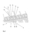
- Fig. 1 shows a known from the prior art and commonly used arrangement.
- a data line 1 is connected to a connection device 2 in addition to several identical data lines.
- the data line 1 has, in addition to a screen 15, a first wire 12 and a second wire 13, which are each surrounded by a cylindrical insulation 16,14.
- the data line 1 has a drain wire 11.
- the printed circuit board 2 has a group of connection pads 3 for the two wires 12, 13 and for the drain wire 11 of the data line 1, namely a first connection pad 31 for the drain wire 11 the first wire 12, a second pad 32 and for the second wire 13, a third pad 33.
- the connection pads 32, 33 of the two wires 12, 13 are next to each other.
- the terminal pad 31 of the drain wire 11 is interposed between the terminal pads of this wire pair 12, 13 and the terminal pads of a pair of wires of an adjacent data line to thereby improve their electrical isolation.
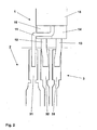
- Fig. 2 shows the same arrangement for the individual data line 1 and for the associated group of connection pads 3 for clarity in a plan view.
- Fig. 3 shows an arrangement according to the invention.
- the edge of the connection device 2 ' is not shown graphically.
- the screen 15 of the data line 1 has a longitudinal section 17. This makes it possible that the two wires 12, 13 are slightly bent away from each other in a set-up area.
- the drain wire 11 is led up between the two insulations 14, 16 and stands in constant mechanical contact with them.
- connection pad 31 'of the drainwire 11 is located between the two connection pads 32', 33 'of the associated pair of wires 12, 13.
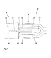
- Fig. 4 Here, it is readily apparent that the two wires 11, 12 are bent away from each other over the length of the slot 17 in the erected area. Furthermore, the beginning of the erected area 41 and the end of the erected area 42 are marked. Also in this illustration, the edge of the connection device 2 'is not shown graphically.
- Fig. 5 represents a cross section through the data line 1 in the normal state, that is, for example, at the beginning 41 of the established area.
- the insulation 14, 16 touch each other.
- the two wires have a distance D to each other.
- the first wire 12 has a distance D1 to the drain wire 11.
- Fig. 6 12 illustrates a cross-section through the data line at the end 42 of the erected area.
- the cores are farther apart from one another according to the slot 17 of the screen than in the aforementioned illustration.
- the cores 12, 13 couple into one another essentially via the drainwire 11. This maintains their effective distance.
- the geometric distance D of the two wires 12, 13 increases in the connection region, the effective distance D1 + D2 remains the same, which reduces the irregularities of the impedance in the connection region.
- Fig. 7 illustrates an electrical device according to the invention with a first group of connection pads 3 ', a second group of connection pads 3 "and a third group of connection pads 3"' in a plan view.
- These groups of connection pads 3 ', 3 ", 3"' have different Distances to a rectilinear edge 21 of the printed circuit board 2, ie at least one group 3 "has a different distance from the rectilinear edge 21 than at least one other group of connection pads 3 ', 3"'. If one looks at a straight line 43 which runs through the first group 3 'and the third group 3'', then it can be seen that the second group 3 "does not lie on this line 43.
- connection pads 3 ', 3 ", 3"' are greatly reduced by their staggered arrangement, since in this way the unshielded parts of a data line 1 ', 1 "' in addition shielded parts of another data line 1 "come to rest.
Landscapes
- Engineering & Computer Science (AREA)
- Microelectronics & Electronic Packaging (AREA)
- Details Of Connecting Devices For Male And Female Coupling (AREA)
- Insulated Conductors (AREA)
- Combinations Of Printed Boards (AREA)
Description
- Die Erfindung betrifft eine Anordnung, bestehend aus einer Anschlussvorrichtung für hochfrequente Datensignale und mindestens einer zum Anschluss daran vorgesehenden Datenleitung, insbesondere einem sogenannten" Twinax"-Kabel, wobei die Datenleitung zur Übertragung hochfrequenter Datensignale von 10 GBit / sek und mehr geeignet ist und drei elektrische Leiter aufweist,nämlich eine erste Ader, eine zweite Ader und ein Drainwire, wobei die beiden Adern jeweils von einer zylinderförmigen Isolierung umgeben sind und wobei die mindestens eine Datenleitung von einem Schirm, beispielsweise von einer zumindest einseitig elektrisch leitenden Schirmfolie, umgeben ist, und wobei die Anschlussvorrichtung für jeden elektrischen Leiter ein Anschlusspad aufweist.
- Dabei sind unter dem Begriff "hochfrequente Digitalsignale" Digitalsignale zu verstehen, deren Bitrate mehr als 10 Gbit / sek., insbesondere sogar 25 Gbit / sek oder mehr beträgt. Derartige Datenleitungen sind unter dem Namen "Twinax" oder "Shielded Twisted Pair" bekannt.
- Weiterhin betrifft die Erfindung ein Verfahren zur Verwendung gemäss dem Anspruch 4 einer Anordnung gemäss dem Ansprüchen 1 bis 3.
- Eine solche Anschlussvorrichtung, beispielsweise eine Leiterplatte oder ein Steckverbinder, und ein solches Anschlussverfahren werden benötigt, um beim Anschluss einer elektrischen Datenleitung im entsprechenden elektrischen Übergang eine möglichst gute Signalintegrität zu gewährleisten.
- Im Stand der Technik ist bereits eine Vielzahl von Lösungen zum Anschluss einer solchen elektrischen Datenleitung bekannt.
- Eine Anordung gemäss dem Oberbegriff des Anspruches 1 ist beispielsweise aus dem Dokument
US2003/064616 bekannt. - So beschreibt die Druckschrift
EP1202419A1 eine entsprechende Anschlussmethode, bei der die Fehlanpassung der differentiellen Impedanz eines Anschlussbereichs des Kabels unter Verwendung eines Schrumpfschlauchs verringert. Dazu wird einem sogenannten "Twisted Pair"-Kabel, dessen beide Leiter im Normalzustand miteinander verdrillt sind, an seinem Anschlussbereich der Schirm entfernt und die beiden Leiter werden mit dazwischen liegendem Drainwire parallel geführt. Durch den Schrumpfschlauch werden gleichbleibende Abstände zwischen den Leitern und dem Drainwire garantiert. Dadurch entsteht im Anschlussbereich eine Twinax-ähnliche Leiterführung. Weiterhin wird offenbart, den Drainwire und das Adernpaar auf unterschiedlichen Seiten der Leiterplatte zu führen und anzuschließen. - Die Druckschrift
US6380485B1 beschreibt eine Anschlusseinheit für ein Twinax-Kabel. Dazu wird eine Leiterplatte vorgeschlagen, an welche das Twinax-Kabel angeschlossen wird, und die eine gute Masseverbindung mit dem dazugehörigen Drainwire ermöglicht. Dazu ist der Drainwire rechtwinklig zu den Leitern umgebogen und in eine Ausnehmung der großflächigen Masseschiene eingefügt. - Weiterhin wird in dieser Druckschrift eine Anordnung als bekannter Stand der Technik erwähnt, bei dem eine Vielzahl von Twinax-Kabeln über einen Leiterplattensteckverbinder konventionell an eine Leiterplatte angeschlossen werden. Daraus wird ersichtlich, dass es bekannt ist, die Leiter auf den dazugehörigen Anschlusspads paarweise nebeneinander anzuordnen und durch deren direkt daneben angeschlossenen Drainwire von dem nächsten Leiterpaar zu trennen.
- Ein Nachteil im Stand der Technik besteht darin, dass für die immer höheren geforderten Datenraten die Homogenität der Einkopplung im elektrischen Übergang zwischen solchen elektrischen Datenleitung und einer daran angeschlossenen elektrischen Einrichtung, beispielsweise einer Leiterplatte oder einem Steckverbinder, in dem dazugehörigen Anschlussbereich nicht ausreichend ist.
- Der Erfindung liegt daher die Aufgabe zugrunde, Impedanzunregelmäßigkeiten im Anschlussbereich zu minimieren.
- Diese Aufgabe wird mit einer Anschlussvorrichtung der eingangs erwähnten Art dadurch gelöst, dass das zum jeweiligen Drainwire gehörende Anschlusspad zwischen den beiden Anschlusspads der beiden zur selben Datenleitung gehörenden Adern angeordnet ist.
- Diese Aufgabe wird weiterhin mit einem Verfahren der eingangs erwähnten Art dadurch gelöst, dass die beiden zu einem Kabel gehörenden Adern mit einem nahezu gleichbleibenden effektiven Abstand bis zu ihren jeweiligen Anschlusspads geführt und dort daran angeschlossen werden.
- Dabei bezeichnet der Begriff "effektiver Abstand zueinander" die Summe eines ersten Abstands und eines zweiten Abstands. Der erste Abstand wird dabei zwischen der ersten Ader und dem Drainwire gemessen und der zweite Abstand wird zwischen der zweiten Ader und dem Drainwire gemessen. Dabei macht man sich die Tatsache zunutze, dass die elektrischen Felder der ersten Ader und der zweiten Ader in starkem Maße über den Drainwire in einander einkoppeln.
- Unter dem Begriff "nahezu gleichbleibender effektiver Abstand zueinander" ist dementsprechend zu verstehen, dass der Drainwire die beiden zylinderförmigen Isolierungen berührt. Der Begriff "nahezu" wird dabei durch die geometrische Qualität des kreisrunden Querschnitts der zylinderförmigen Isolierung festgelegt.
- Vorteilhafte Ausgestaltungen der Erfindung sind in den Unteransprüchen angegeben.
- Bei der Erfindung handelt es sich um eine Vorrichtung, die benötigt wird, um die Signalintegrität von hochfrequenten Datenübertragungen zu verbessern.
- Ein Vorteil der vorliegenden Erfindung besteht darin, dass sich die Unregelmäßigkeiten der elektrischen Impedanz im Anschlussbereich verringern, wodurch eine gute Einkopplung gegeben ist und hohe Datenraten über diesen Anschluss übertragbar sind.
- Ein weiterer Vorteil besteht darin, dass der Anschluss des elektrischen Datenleitung händisch mit vertretbarem Aufwand erfolgen kann.
- Beispielsweise kann der Schirm, insbesondere beim Abisolieren, einen Längsschnitt erfahren. Das Kabel wird dann zur Leiterplatte ausgerichtet. Dabei wird durch den Längsschlitz ermöglicht, die Kabel auf die Leiterplattenebene herunterzudrücken, wobei der Drainwire die zylindrischen Isolierungen auseinander schiebt.
- Ein entsprechendes Werkzeug kann zum Hinunterdrücken eingesetzt werden. Dieses Werkzeug weist Führungsrippen auf, welche die Isolierungen und damit die elektrischen Leiter führen und ausrichten.
- In einer weiteren vorteilhaften Ausführung weist die Anschlusseinrichtung mindestens zwei Gruppen von Anschlusspads auf, die versetzt gegeneinander angeordnet sind. Unter einer "Gruppe von Anschlusspads" sind dabei drei Anschlusspads zu verstehen, die für den Anschluss dreier elektrischer Leiter einer Datenleitung vorgesehen sind. Die Anschlussvorrichtung besitzt in ihrer Anschlussrichtung, d.h. in derjenigen Richtung, aus der die Datenleitungen auf die Anschlusseinrichtung geführt sind, einen geradlinigen Rand. Aus der versetzten Anordnung ergibt sich somit, dass mindestens eine Gruppe von Anschlusspads einen anderen Abstand zu dem geradlinigen Rand besitzt als zumindest eine andere Gruppe von Anschlusspads.
- In einer weiteren Ausführungsform weist die Anschlusseinrichtung mehr als zwei Gruppen von Anschlusspads auf. Dann ergibt sich aus der versetzen Anordnung, dass die Anordnung der Gruppen von Anschlusspads auf der Leiterplatte von einer geradlinigen Anordnung abweicht. Dabei bezeichnet der Begriff "geradlinige Anordnung" eine Anordnung, in der die Gruppen von Anschlusspads auf der Leiterplatte in einer Reihe angeordnet sind, d.h. auf einer geraden Linie liegen. Dementsprechend bedeutet das Kennzeichen "dass die Anordnung der Gruppen von Anschlusspads auf der Leiterplatte von einer geradlinigen Anordnung abweicht", dass mindestens eine Gruppe von Anschlusspads nicht auf der geraden Linie liegt, welche durch mindestens zwei andere Gruppen von Anschlusspads verläuft.
- Ein Vorteil dieser Ausführung besteht darin, dass das Übersprechen zwischen den verschiedenen Gruppen von Anschlusspads stark reduziert ist.
- Ein weiterer zusätzlicher Vorteil dieser Ausführungsform besteht darin, dass gerade bei einer großen Anzahl von Datenleitungen deren Laufzeitunterschiede ausgleichbar sind, weil Wegdifferenzen problemlos ausgeglichen werden können. Dies spielt eine große Rolle, weil gerade im Bereich der hochfrequenten Datenübertragung bereits Kabellängenunterschiede im Millimeterbereich bis hin zum Zentimeterbereich zu relevanten Laufzeitunterschieden führen können, was die Anschlusstechnik üblicherweise erheblich erschwert.
- In einer bevorzugten Ausführungsform handelt es sich bei der Anschlussvorrichtung um eine Leiterplatte.
- In einer weiteren vorteilhaften Ausgestaltung können die Datenleitungen beispielsweise mit doppeltseitigem Klebeband auf der Anschlusseinrichtung, insbesondere auf einer Leiterplatte, befestigt uns später gemeinsam mit weiteren Komponenten in einem Vergießvorgang mit einer Vergussmasse vergossen zu werden.
- In einer bevorzugten Ausführungsform handelt es sich bei der Anschlussvorrichtung um einen Steckverbinder oder zumindest um einen Teil eines Steckverbinders.
- Ein Ausführungsbeispiel der Erfindung ist in der Zeichnung dargestellt und wird im Folgenden näher erläutert. Es zeigen:
-
Fig. 1 eine Anschlussvorrichtung gemäß dem Stand der Technik mit mehreren daran angeschlossenen elektrischen Datenleitungen in einer schrägen Draufsicht; -
Fig. 2 einen Teil der Anschlussvorrichtung gemäß dem Stand der Technik mit einer der daran angeschlossenen elektrischen Datenleitungen in einer Draufsicht; -
Fig. 3 eine erfindungsgemäße Anschlussvorrichtung mit der daran angeschlossenen elektrischen Datenleitung in einer schrägen Draufsicht; -
Fig. 4 eine erfindungsgemäße Anschlussvorrichtung mit der daran angeschlossenen elektrischen Datenleitung in einer Draufsicht; -
Fig. 5 einen Querschnitt durch einen nicht abisolierten Bereich der elektrischen Datenleitung; -
Fig. 6 einen Querschnitt durch den Übergang zwischen einem aufgestellten Bereich und einem abisolierten Bereich der elektrischen Datenleitung; -
Fig. 7 eine erfindungsgemäße elektrische Einrichtung mit mehreren versetzt angeordneten Gruppen von Anschlusspads. -
Fig. 1 zeigt eine aus dem Stand der Technik bekannte und üblicherweise verwendete Anordnung. Dabei wird eine Datenleitung 1 neben mehreren gleichen Datenleitungen an eine Anschlusseinrichtung 2 angeschlossen. Die Datenleitung 1 besitzt neben einem Schirm 15 eine erste Ader 12 und eine zweite Ader 13, die jeweils von einer zylindrischen Isolierung 16,14 umgeben sind. Weiterhin besitzt die Datenleitung 1 einen Beilaufdraht ("Drainwire") 11. Die Leiterplatte 2 besitzt für die beiden Adern 12, 13 sowie für den Drainwire 11 der Datenleitung 1 eine Gruppe von Anschlusspads 3, nämlich für den Drainwire 11 ein erstes Anschlusspad 31, für die erste Ader 12 ein zweites Anschlusspad 32 und für die zweite Ader 13 ein drittes Anschlusspad 33. Dabei liegen die Anschlusspads 32, 33 der beiden Adern 12, 13 direkt neben einander. Das Anschlusspad 31 des Drainwires 11 liegt zwischen den Anschlusspads dieses Adernpaars 12, 13 und den Anschlusspads eines Adernpaars einer benachbarten Datenleitung, um dadurch deren elektrische Trennung zu verbessern. -
Fig. 2 zeigt dieselbe Anordnung für die einzelne Datenleitung 1 und für die dazugehörige Gruppe von Anschlusspads 3 zur besseren Übersichtlichkeit in einer Draufsicht. -
Fig. 3 zeigt eine erfindungsgemäße Anordnung. Dabei ist der Rand der Anschlussvorrichtung 2' nicht graphisch dargestellt. Der Schirm 15 der Datenleitung 1 weist einen Längsschnitt 17 auf. Dadurch wird es ermöglicht, dass die beiden Adern 12, 13 in einem aufgestellten Bereich leicht von einander weggebogen sind. Der Drainwire 11 wird zwischen den beiden Isolierungen 14, 16 hochgeführt und steht dabei im ständigen mechanischen Kontakt mit diesen. - Dementsprechend befindet sich das Anschlusspad 31' des Drainwires 11 zwischen den beiden Anschlusspads 32', 33' des dazugehörigen Adernpaars 12,13.
-
Fig. 4 stellt die vorgenannte Anordnung zur besseren Übersichtlichkeit in einer Draufsicht dar. Dabei ist gut erkennbar, dass sich die beiden Adern 11,12 über die Länge des Schlitzes 17 in dem aufgestellten Bereich voneinander weggebogen sind. Weiterhin ist der Anfang des aufgestellten Bereiches 41 und das Ende des aufgestellten Bereiches 42 gekennzeichnet. Auch in dieser Darstellung ist der Rand der Anschlussvorrichtung 2' nicht graphisch dargestellt. -
Fig. 5 stellt einen Querschnitt durch die Datenleitung 1 im Normalzustand, also beispielsweise am Anfang 41 des aufgestellten Bereiches dar. Die Isolierungen 14, 16 berühren sich. Die beiden Adern besitzen einen Abstand D zueinander. Die erste Ader 12 besitzt einen Abstand D1 zum Drainwire 11. Die zweite Ader 13 besitzt einen Abstand D2 zum Drainwire 11. Da der Drainwire 11 die beiden zylindrischen Isolierungen 14, 16 berührt, gilt für den effektiven Anstand: D1 + D2 = D. -
Fig. 6 stellt einen Querschnitt durch die Datenleitung am Ende 42 des aufgestellten Bereiches dar. Die Adern sind entsprechend dem Schlitz 17 des Schirms weiter von einander entfernt als in der vorgenannten Darstellung. Die Adern 12, 13 koppeln im Wesentlichen über den Drainwire 11 in einander ein. Dadurch bleibt ihr effektiver Abstand erhalten. Obwohl sich der geometrische Abstand D der beiden Adern 12, 13 im Anschlussbereich vergrößert, bleibt der Effektive Abstand D1 + D2 gleich, wodurch sich die Unregelmäßigkeiten der Impedanz im Anschlussbereich verringern. -
Fig. 7 stellt eine erfindungsgemäße elektrische Einrichtung mit einer ersten Gruppe von Anschlusspads 3', einer zweiten Gruppe von Anschlusspads 3" und einer dritten Gruppe von Anschlusspads 3"' in einer Draufsicht dar. Diese Gruppen von Anschlusspads 3',3" ,3"' besitzen unterschiedliche Abstände zu einem geradlinigen Rand 21 der Leiterplatte 2, d.h. mindestens eine Gruppe 3" besitzt einen anderen Abstand zum geradlinigen Rand 21 als zumindest eine andere Gruppe von Anschlusspads 3',3"'. Betrachten man eine gerade Linie 43, welche durch die erste Gruppe 3' und die dritte Gruppe 3'" verläuft, so ist erkennbar, dass die zweite Gruppe 3" nicht auf dieser Linie 43 liegt. - Aus dieser Darstellung wird ersichtlich, dass ein elektrisches Übersprechen zwischen den verschiedenen Gruppen von Anschlusspads 3',3",3"' durch deren versetzte Anordnung stark reduziert ist, da auf diese Weise die nicht geschirmten Teile einer Datenleitung 1',1"' neben geschirmten Teilen einer anderen Datenleitung 1" zu liegen kommen.
-
- 1
- Datenleitung
- 11
- Drainwire
- 12
- erste Ader
- 13
- zweite Ader
- 14
- zylindrische Isolierung der zweiten Ader
- 15
- Schirm
- 16
- zylindrische Isolierung der ersten Ader
- 17
- Längsschlitz
- 2,2'
- Anschlussvorrichtung
- 21
- geradliniger Rand der Anschlussvorrichtung
- 3
- Gruppe von Anschlusspads
- 31
- Anschlusspad des Drainwires
- 32
- Anschlusspad der ersten Ader
- 33
- Anschlusspad der zweiten Ader
Claims (6)
- Anordnung, bestehend aus einer Anschlussvorrichtung (2) für hochfrequente Datensignale und mindestens einer zum Anschluss daran vorgesehenden Datenleitung (1), insbesondere einem sogenannten "Twinax"-Kabel, wobei die Datenleitung (1) zur Übertragung hochfrequenter Datensignale von 10 GBit / sek und mehr geeignet ist und drei elektrische Leiter aufweist, nämlich eine erste Ader (12), eine zweite Ader (13) und ein Drainwire (11), wobei die beiden Adern (12,13) jeweils von einer zylinderförmigen Isolierung (14,16) umgeben sind und wobei die mindestens eine Datenleitung (1) von einem Schirm (15), beispielsweise von einer zumindest einseitig elektrisch leitenden Schirmfolie, umgeben ist, und wobei die Anschlussvorrichtung (2) für jeden elektrischen Leiter ein Anschlusspad (31,32,33) aufweist, dadurch gekennzeichnet,
dass das zum jeweiligen Drainwire (11) gehörende Anschlusspad (31') zwischen den beiden Anschlusspads (32',33') der beiden zur selben Datenleitung (1) gehörenden Adern (12,13) angeordnet ist,
wobei der Schirm (15) der Datenleitung (1) einen Längsschnitt (17) aufweist und wobei die beiden Adern (12,13) in einem aufgestellten Bereich, welcher einen Anfang (41) und eine Ende (42) besitzt, leicht voneinander weggebogen sind und dass der Drainwire (11) in diesem aufgestellten Bereich zwischen den beiden Isolierungen (14, 16) hochgeführt wird und in einem ständigen mechanischen Kontakt mit den dazugehörigen Isolierungen (14,16) steht. - Anordnung nach Anspruch 1, dadurch gekennzeichnet, dass die Anschlussvorrichtung (2') mindestens zwei Gruppen von Anschlusspads (3',3",3"') aufweist, wobei jede Gruppe von Anschlusspads (3',3",3"') zum Anschluss der elektrischen Leiter (11,12,13) jeweils einer Datenleitung (1',1",1"') vorgesehen ist, wobei die Anschlussvorrichtung (2') in ihrer Anschlussrichtung einen geradlinigen Rand (21) aufweist, und dass mindestens eine Gruppe von Anschlusspads (3',3"') einen anderen Abstand zu dem geradlinigen Rand (21) besitzt als zumindest eine andere Gruppe (3") von Anschlusspads.
- Anordnung nach Anspruch 1, dadurch gekennzeichnet, dass die Anschlussvorrichtung (2') mindestens drei Gruppen von Anschlusspads (3',3",3"') aufweist, wobei jede Gruppe von Anschlusspads (3',3",3"') zum Anschluss der elektrischen Leiter (11,12,13) jeweils einer Datenleitung (1',1",1") vorgesehen ist und dass die Anordnung der Gruppen von Anschlusspads (3',3",3"') auf der Anschlussvorrichtung (2') von einer geradlinigen Anordnung abweicht.
- Verfahren zur Verwendung einer Anordnung nach einem der Ansprüche 1 bis 3, dadurch gekennzeichnet,
dass die beiden Adern (12,13) in dem aufgestellten Bereich voneinander weggebogen werden, indem der Drainwire (11) die dazugehörigen Isolierungen auseinander schiebt. - Verfahren nach Anspruch 4,
gekennzeichnet dadurch, dass die beiden Adern (12,13) im Bereich des Längsschlitzes (17) leicht auseinander gebogen werden. - Verfahren nach Anspruch 5,
dadurch gekennzeichnet, dass der Drainwire (11) im Bereich des Längsschlitzes (17) zwischen die Isolierungen (14,16) der beiden Adern (12,13) gedrückt wird, und somit für einen nahezu gleichbleibenden effektiven Abstand (D1+D2) zwischen den Adern (12,13) sorgt.
Applications Claiming Priority (2)
| Application Number | Priority Date | Filing Date | Title |
|---|---|---|---|
| DE102011001225A DE102011001225A1 (de) | 2011-03-11 | 2011-03-11 | Anschlussvorrichtung und Anschlussverfahren für hochfrequente Digitalsignale |
| PCT/DE2012/100044 WO2012122974A1 (de) | 2011-03-11 | 2012-02-22 | Anschlussvorrichtung und anschlussverfahren für hochfrequente digitalsignale |
Publications (2)
| Publication Number | Publication Date |
|---|---|
| EP2684253A1 EP2684253A1 (de) | 2014-01-15 |
| EP2684253B1 true EP2684253B1 (de) | 2015-04-22 |
Family
ID=46061964
Family Applications (1)
| Application Number | Title | Priority Date | Filing Date |
|---|---|---|---|
| EP20120720401 Active EP2684253B1 (de) | 2011-03-11 | 2012-02-22 | Anschlussvorrichtung und anschlussverfahren für hochfrequente digitalsignale |
Country Status (6)
| Country | Link |
|---|---|
| US (1) | US9161436B2 (de) |
| EP (1) | EP2684253B1 (de) |
| JP (1) | JP5705339B2 (de) |
| CN (1) | CN103415959B (de) |
| DE (1) | DE102011001225A1 (de) |
| WO (1) | WO2012122974A1 (de) |
Families Citing this family (15)
| Publication number | Priority date | Publication date | Assignee | Title |
|---|---|---|---|---|
| US9049787B2 (en) * | 2013-01-18 | 2015-06-02 | Molex Incorporated | Paddle card with improved performance |
| CN106165201B (zh) * | 2014-04-02 | 2020-05-12 | 莫列斯有限公司 | 线缆端接结构 |
| WO2016149266A1 (en) | 2015-03-18 | 2016-09-22 | Fci Asia Pte. Ltd | Electrical cable assembly |
| EP3121909B1 (de) * | 2015-07-21 | 2018-09-19 | Delphi Technologies, Inc. | Elektrischer verbinder mit angepasster impedanz |
| US11374361B2 (en) * | 2018-02-16 | 2022-06-28 | Junkosha Inc. | Plug connector, connector system, and flying body |
| US20190260165A1 (en) * | 2018-02-16 | 2019-08-22 | The Siemon Company | Cable termination for connectors |
| US10643766B1 (en) * | 2018-10-22 | 2020-05-05 | Dell Products L.P. | Drain-aligned cable and method for forming same |
| US11228123B2 (en) | 2018-12-17 | 2022-01-18 | Amphenol Corporation | High performance cable termination |
| JP6986596B2 (ja) * | 2019-06-14 | 2021-12-22 | センサービュー・インコーポレイテッドSensorview Incorporated | 超高周波信号伝送用小型コネクタ |
| TWM604961U (zh) * | 2020-07-30 | 2020-12-01 | 貿聯國際股份有限公司 | 用於電路板的金屬箔片及具有該金屬箔片的電路裝置 |
| CN112018549A (zh) * | 2020-08-28 | 2020-12-01 | 重庆邮电大学 | 一种适用于麻花针高速传输的外壳 |
| CN113260147B (zh) * | 2021-05-26 | 2025-06-03 | 京东方科技集团股份有限公司 | 电路板、显示装置 |
| CN116073195A (zh) * | 2023-02-27 | 2023-05-05 | 苏州浪潮智能科技有限公司 | Ocp网卡线缆的ncsi信号优化装置及其制备方法 |
| DE102023117404A1 (de) * | 2023-06-30 | 2025-01-02 | Ifm Electronic Gmbh | Verfahren zur Herstellung einer Leiterplatte mit einem Anschlusskabel |
| WO2025040974A1 (en) * | 2023-08-22 | 2025-02-27 | 3M Innovative Properties Company | Cable assembly |
Family Cites Families (18)
| Publication number | Priority date | Publication date | Assignee | Title |
|---|---|---|---|---|
| US4508415A (en) | 1983-07-29 | 1985-04-02 | Amp Incorporated | Shielded electrical connector for flat cable |
| US5176538A (en) * | 1991-12-13 | 1993-01-05 | W. L. Gore & Associates, Inc. | Signal interconnector module and assembly thereof |
| CH695034A5 (de) * | 1998-09-30 | 2005-11-15 | Reichle & De Massari Fa | Steckverbindungsteil einer Steckverbindung fuer hochfrequente Datenuebertragung ueber elektrische Leiter. |
| TW456619U (en) * | 1999-07-16 | 2001-09-21 | Molex Inc | Impedance-tuned termination assembly and connectors incorporating same |
| US6217372B1 (en) | 1999-10-08 | 2001-04-17 | Tensolite Company | Cable structure with improved grounding termination in the connector |
| US6857899B2 (en) * | 1999-10-08 | 2005-02-22 | Tensolite Company | Cable structure with improved grounding termination in the connector |
| US6380485B1 (en) | 2000-08-08 | 2002-04-30 | International Business Machines Corporation | Enhanced wire termination for twinax wires |
| JP3645170B2 (ja) | 2000-10-27 | 2005-05-11 | タイコエレクトロニクスアンプ株式会社 | 電気ケーブル端部構造および電気ケーブル端部処理方法 |
| NL1018175C2 (nl) * | 2001-05-30 | 2002-12-03 | Fci Mechelen N V | Stekkerblok en kabelconnector. |
| JP2003346987A (ja) * | 2002-05-27 | 2003-12-05 | Fujikura Ltd | コネクタ付き集合ケーブル |
| JP4083499B2 (ja) * | 2002-08-07 | 2008-04-30 | 株式会社フジクラ | 伝送ケーブルの接続方法及びコネクタ |
| US6739904B2 (en) | 2002-10-04 | 2004-05-25 | Hon Hai Precision Ind. Co., Ltd. | Cable connector assembly |
| JP2004134128A (ja) * | 2002-10-08 | 2004-04-30 | Fujikura Ltd | コネクタ及び伝送ケーブルの接続方法並びにその接続構造 |
| US6955565B2 (en) | 2002-12-30 | 2005-10-18 | Molex Incorporated | Cable connector with shielded termination area |
| CN102082367B (zh) * | 2004-03-12 | 2013-11-20 | 泛达公司 | 减小电连接器中串扰的方法及装置 |
| JP4216287B2 (ja) | 2006-02-20 | 2009-01-28 | 日本航空電子工業株式会社 | コネクタ |
| US9124009B2 (en) * | 2008-09-29 | 2015-09-01 | Amphenol Corporation | Ground sleeve having improved impedance control and high frequency performance |
| US8696378B2 (en) * | 2012-02-24 | 2014-04-15 | Tyco Electronics Corporation | Electrical connector assembly and printed circuit board configured to electrically couple to a communication cable |
-
2011
- 2011-03-11 DE DE102011001225A patent/DE102011001225A1/de not_active Ceased
-
2012
- 2012-02-22 JP JP2013558304A patent/JP5705339B2/ja not_active Expired - Fee Related
- 2012-02-22 CN CN201280012776.4A patent/CN103415959B/zh active Active
- 2012-02-22 US US14/002,081 patent/US9161436B2/en active Active
- 2012-02-22 EP EP20120720401 patent/EP2684253B1/de active Active
- 2012-02-22 WO PCT/DE2012/100044 patent/WO2012122974A1/de not_active Ceased
Also Published As
| Publication number | Publication date |
|---|---|
| WO2012122974A1 (de) | 2012-09-20 |
| DE102011001225A1 (de) | 2012-09-13 |
| US20150144391A1 (en) | 2015-05-28 |
| JP2014509770A (ja) | 2014-04-21 |
| JP5705339B2 (ja) | 2015-04-22 |
| US9161436B2 (en) | 2015-10-13 |
| CN103415959B (zh) | 2016-03-16 |
| EP2684253A1 (de) | 2014-01-15 |
| CN103415959A (zh) | 2013-11-27 |
Similar Documents
| Publication | Publication Date | Title |
|---|---|---|
| EP2684253B1 (de) | Anschlussvorrichtung und anschlussverfahren für hochfrequente digitalsignale | |
| EP3170229B1 (de) | Steckverbinder und bauelement und verwendung des steckverbinders | |
| WO2009138168A1 (de) | Leiterplatte für elektrischen verbinder und elektrischer verbinder | |
| EP2375501B1 (de) | Steckverbinder zur Aufnahme eines mehradrigen Kabels | |
| EP2797175B1 (de) | Stecker für ein mehrere Adern aufweisendes Daten- und/oder Telekommunikations-Kabel | |
| DE19853666A1 (de) | Elektrischer Verbinder mit Kompensationseinsatz | |
| EP2957003B1 (de) | Adapter | |
| DE102008027512A1 (de) | Steckverbinder und Verfahren zum Anschluss von elektrischen Leitern an einem Steckverbinder | |
| EP2044654B1 (de) | Verbinderblock | |
| EP2047571B1 (de) | Steckverbinder für die Telekommunikations- und Datentechnik | |
| DE69931591T2 (de) | Leiterplatte für Modularstecker | |
| EP3080872B1 (de) | Kontaktanbindung von geschirmten datenleitungen an einer platine sowie verfahren zur kontaktierung mehrerer geschirmter datenleitungen an einer platine | |
| EP2290753B1 (de) | Steckverbinder und Multilayerplatine | |
| EP2417675B1 (de) | Steckersystemgehäuse für mehradrige kabel | |
| DE102010034790B4 (de) | Kontaktträger für wenigstens eine Vorrichtung zur Kontaktierung eines elektrischen Leiters mit einer Leiterbahn | |
| EP0954076A2 (de) | Hochleistungstelekommunikations-/Datenverbindung und -verbinder mit hoher Kontaktdichte mit Abgriff und Kontaktverdrängungsbaugruppe | |
| EP3163688B1 (de) | Anordnung mit zwei über ein verbindungselement miteinander verbundenen datenkabeln | |
| DE20203910U1 (de) | Anschlussmodul der Telekommunikationstechnik | |
| DE102009010930B4 (de) | Verfahren zum Einspleißen einer Doppelader in mindestens eine bestehende Endteilnehmer-Doppelader und Aderverbinder | |
| DE102007002177A1 (de) | Verbindungsaufbau für ein abgeschirmtes Kabel | |
| EP3367514A1 (de) | Steckverbindung für hochfrequenzanwendungen, zum beispiel für ethernet anwendung | |
| EP2207244A2 (de) | Steckverbinder und Multilayerplatine | |
| EP1168526B1 (de) | Leiterplattensteckverbindung | |
| DE102016008679A1 (de) | Adapter und Kabel mit Adapter | |
| DE102018121582A1 (de) | Elektrische Verteilervorrichtung, Montageverfahren und Signalübertragungssystem |
Legal Events
| Date | Code | Title | Description |
|---|---|---|---|
| PUAI | Public reference made under article 153(3) epc to a published international application that has entered the european phase |
Free format text: ORIGINAL CODE: 0009012 |
|
| 17P | Request for examination filed |
Effective date: 20130805 |
|
| AK | Designated contracting states |
Kind code of ref document: A1 Designated state(s): AL AT BE BG CH CY CZ DE DK EE ES FI FR GB GR HR HU IE IS IT LI LT LU LV MC MK MT NL NO PL PT RO RS SE SI SK SM TR |
|
| DAX | Request for extension of the european patent (deleted) | ||
| GRAP | Despatch of communication of intention to grant a patent |
Free format text: ORIGINAL CODE: EPIDOSNIGR1 |
|
| INTG | Intention to grant announced |
Effective date: 20141119 |
|
| GRAS | Grant fee paid |
Free format text: ORIGINAL CODE: EPIDOSNIGR3 |
|
| GRAA | (expected) grant |
Free format text: ORIGINAL CODE: 0009210 |
|
| AK | Designated contracting states |
Kind code of ref document: B1 Designated state(s): AL AT BE BG CH CY CZ DE DK EE ES FI FR GB GR HR HU IE IS IT LI LT LU LV MC MK MT NL NO PL PT RO RS SE SI SK SM TR |
|
| REG | Reference to a national code |
Ref country code: GB Ref legal event code: FG4D Free format text: NOT ENGLISH |
|
| REG | Reference to a national code |
Ref country code: CH Ref legal event code: EP |
|
| REG | Reference to a national code |
Ref country code: AT Ref legal event code: REF Ref document number: 723744 Country of ref document: AT Kind code of ref document: T Effective date: 20150515 |
|
| REG | Reference to a national code |
Ref country code: IE Ref legal event code: FG4D Free format text: LANGUAGE OF EP DOCUMENT: GERMAN |
|
| REG | Reference to a national code |
Ref country code: DE Ref legal event code: R096 Ref document number: 502012002932 Country of ref document: DE Effective date: 20150603 |
|
| REG | Reference to a national code |
Ref country code: NL Ref legal event code: VDEP Effective date: 20150422 |
|
| REG | Reference to a national code |
Ref country code: LT Ref legal event code: MG4D |
|
| PG25 | Lapsed in a contracting state [announced via postgrant information from national office to epo] |
Ref country code: NL Free format text: LAPSE BECAUSE OF FAILURE TO SUBMIT A TRANSLATION OF THE DESCRIPTION OR TO PAY THE FEE WITHIN THE PRESCRIBED TIME-LIMIT Effective date: 20150422 |
|
| PG25 | Lapsed in a contracting state [announced via postgrant information from national office to epo] |
Ref country code: HR Free format text: LAPSE BECAUSE OF FAILURE TO SUBMIT A TRANSLATION OF THE DESCRIPTION OR TO PAY THE FEE WITHIN THE PRESCRIBED TIME-LIMIT Effective date: 20150422 Ref country code: ES Free format text: LAPSE BECAUSE OF FAILURE TO SUBMIT A TRANSLATION OF THE DESCRIPTION OR TO PAY THE FEE WITHIN THE PRESCRIBED TIME-LIMIT Effective date: 20150422 Ref country code: LT Free format text: LAPSE BECAUSE OF FAILURE TO SUBMIT A TRANSLATION OF THE DESCRIPTION OR TO PAY THE FEE WITHIN THE PRESCRIBED TIME-LIMIT Effective date: 20150422 Ref country code: NO Free format text: LAPSE BECAUSE OF FAILURE TO SUBMIT A TRANSLATION OF THE DESCRIPTION OR TO PAY THE FEE WITHIN THE PRESCRIBED TIME-LIMIT Effective date: 20150722 Ref country code: PT Free format text: LAPSE BECAUSE OF FAILURE TO SUBMIT A TRANSLATION OF THE DESCRIPTION OR TO PAY THE FEE WITHIN THE PRESCRIBED TIME-LIMIT Effective date: 20150824 Ref country code: FI Free format text: LAPSE BECAUSE OF FAILURE TO SUBMIT A TRANSLATION OF THE DESCRIPTION OR TO PAY THE FEE WITHIN THE PRESCRIBED TIME-LIMIT Effective date: 20150422 |
|
| PG25 | Lapsed in a contracting state [announced via postgrant information from national office to epo] |
Ref country code: IS Free format text: LAPSE BECAUSE OF FAILURE TO SUBMIT A TRANSLATION OF THE DESCRIPTION OR TO PAY THE FEE WITHIN THE PRESCRIBED TIME-LIMIT Effective date: 20150822 Ref country code: RS Free format text: LAPSE BECAUSE OF FAILURE TO SUBMIT A TRANSLATION OF THE DESCRIPTION OR TO PAY THE FEE WITHIN THE PRESCRIBED TIME-LIMIT Effective date: 20150422 Ref country code: GR Free format text: LAPSE BECAUSE OF FAILURE TO SUBMIT A TRANSLATION OF THE DESCRIPTION OR TO PAY THE FEE WITHIN THE PRESCRIBED TIME-LIMIT Effective date: 20150723 Ref country code: LV Free format text: LAPSE BECAUSE OF FAILURE TO SUBMIT A TRANSLATION OF THE DESCRIPTION OR TO PAY THE FEE WITHIN THE PRESCRIBED TIME-LIMIT Effective date: 20150422 |
|
| REG | Reference to a national code |
Ref country code: FR Ref legal event code: PLFP Year of fee payment: 5 |
|
| REG | Reference to a national code |
Ref country code: DE Ref legal event code: R097 Ref document number: 502012002932 Country of ref document: DE |
|
| PG25 | Lapsed in a contracting state [announced via postgrant information from national office to epo] |
Ref country code: EE Free format text: LAPSE BECAUSE OF FAILURE TO SUBMIT A TRANSLATION OF THE DESCRIPTION OR TO PAY THE FEE WITHIN THE PRESCRIBED TIME-LIMIT Effective date: 20150422 Ref country code: DK Free format text: LAPSE BECAUSE OF FAILURE TO SUBMIT A TRANSLATION OF THE DESCRIPTION OR TO PAY THE FEE WITHIN THE PRESCRIBED TIME-LIMIT Effective date: 20150422 |
|
| PLBE | No opposition filed within time limit |
Free format text: ORIGINAL CODE: 0009261 |
|
| STAA | Information on the status of an ep patent application or granted ep patent |
Free format text: STATUS: NO OPPOSITION FILED WITHIN TIME LIMIT |
|
| PG25 | Lapsed in a contracting state [announced via postgrant information from national office to epo] |
Ref country code: CZ Free format text: LAPSE BECAUSE OF FAILURE TO SUBMIT A TRANSLATION OF THE DESCRIPTION OR TO PAY THE FEE WITHIN THE PRESCRIBED TIME-LIMIT Effective date: 20150422 Ref country code: PL Free format text: LAPSE BECAUSE OF FAILURE TO SUBMIT A TRANSLATION OF THE DESCRIPTION OR TO PAY THE FEE WITHIN THE PRESCRIBED TIME-LIMIT Effective date: 20150422 Ref country code: SK Free format text: LAPSE BECAUSE OF FAILURE TO SUBMIT A TRANSLATION OF THE DESCRIPTION OR TO PAY THE FEE WITHIN THE PRESCRIBED TIME-LIMIT Effective date: 20150422 Ref country code: RO Free format text: LAPSE BECAUSE OF NON-PAYMENT OF DUE FEES Effective date: 20150422 |
|
| 26N | No opposition filed |
Effective date: 20160125 |
|
| PG25 | Lapsed in a contracting state [announced via postgrant information from national office to epo] |
Ref country code: IT Free format text: LAPSE BECAUSE OF FAILURE TO SUBMIT A TRANSLATION OF THE DESCRIPTION OR TO PAY THE FEE WITHIN THE PRESCRIBED TIME-LIMIT Effective date: 20150422 |
|
| PG25 | Lapsed in a contracting state [announced via postgrant information from national office to epo] |
Ref country code: SI Free format text: LAPSE BECAUSE OF FAILURE TO SUBMIT A TRANSLATION OF THE DESCRIPTION OR TO PAY THE FEE WITHIN THE PRESCRIBED TIME-LIMIT Effective date: 20150422 Ref country code: BE Free format text: LAPSE BECAUSE OF NON-PAYMENT OF DUE FEES Effective date: 20160229 |
|
| PG25 | Lapsed in a contracting state [announced via postgrant information from national office to epo] |
Ref country code: LU Free format text: LAPSE BECAUSE OF FAILURE TO SUBMIT A TRANSLATION OF THE DESCRIPTION OR TO PAY THE FEE WITHIN THE PRESCRIBED TIME-LIMIT Effective date: 20160222 Ref country code: MC Free format text: LAPSE BECAUSE OF FAILURE TO SUBMIT A TRANSLATION OF THE DESCRIPTION OR TO PAY THE FEE WITHIN THE PRESCRIBED TIME-LIMIT Effective date: 20150422 |
|
| REG | Reference to a national code |
Ref country code: CH Ref legal event code: PL |
|
| GBPC | Gb: european patent ceased through non-payment of renewal fee |
Effective date: 20160222 |
|
| PG25 | Lapsed in a contracting state [announced via postgrant information from national office to epo] |
Ref country code: LI Free format text: LAPSE BECAUSE OF NON-PAYMENT OF DUE FEES Effective date: 20160229 Ref country code: CH Free format text: LAPSE BECAUSE OF NON-PAYMENT OF DUE FEES Effective date: 20160229 |
|
| REG | Reference to a national code |
Ref country code: IE Ref legal event code: MM4A |
|
| REG | Reference to a national code |
Ref country code: FR Ref legal event code: PLFP Year of fee payment: 6 |
|
| PG25 | Lapsed in a contracting state [announced via postgrant information from national office to epo] |
Ref country code: GB Free format text: LAPSE BECAUSE OF NON-PAYMENT OF DUE FEES Effective date: 20160222 Ref country code: IE Free format text: LAPSE BECAUSE OF NON-PAYMENT OF DUE FEES Effective date: 20160222 |
|
| PG25 | Lapsed in a contracting state [announced via postgrant information from national office to epo] |
Ref country code: SE Free format text: LAPSE BECAUSE OF FAILURE TO SUBMIT A TRANSLATION OF THE DESCRIPTION OR TO PAY THE FEE WITHIN THE PRESCRIBED TIME-LIMIT Effective date: 20150422 |
|
| PG25 | Lapsed in a contracting state [announced via postgrant information from national office to epo] |
Ref country code: MT Free format text: LAPSE BECAUSE OF FAILURE TO SUBMIT A TRANSLATION OF THE DESCRIPTION OR TO PAY THE FEE WITHIN THE PRESCRIBED TIME-LIMIT Effective date: 20150422 |
|
| REG | Reference to a national code |
Ref country code: FR Ref legal event code: PLFP Year of fee payment: 7 |
|
| REG | Reference to a national code |
Ref country code: AT Ref legal event code: MM01 Ref document number: 723744 Country of ref document: AT Kind code of ref document: T Effective date: 20170222 |
|
| PG25 | Lapsed in a contracting state [announced via postgrant information from national office to epo] |
Ref country code: HU Free format text: LAPSE BECAUSE OF FAILURE TO SUBMIT A TRANSLATION OF THE DESCRIPTION OR TO PAY THE FEE WITHIN THE PRESCRIBED TIME-LIMIT; INVALID AB INITIO Effective date: 20120222 Ref country code: AT Free format text: LAPSE BECAUSE OF NON-PAYMENT OF DUE FEES Effective date: 20170222 Ref country code: SM Free format text: LAPSE BECAUSE OF FAILURE TO SUBMIT A TRANSLATION OF THE DESCRIPTION OR TO PAY THE FEE WITHIN THE PRESCRIBED TIME-LIMIT Effective date: 20150422 Ref country code: CY Free format text: LAPSE BECAUSE OF FAILURE TO SUBMIT A TRANSLATION OF THE DESCRIPTION OR TO PAY THE FEE WITHIN THE PRESCRIBED TIME-LIMIT Effective date: 20150422 |
|
| PG25 | Lapsed in a contracting state [announced via postgrant information from national office to epo] |
Ref country code: MK Free format text: LAPSE BECAUSE OF FAILURE TO SUBMIT A TRANSLATION OF THE DESCRIPTION OR TO PAY THE FEE WITHIN THE PRESCRIBED TIME-LIMIT Effective date: 20150422 Ref country code: TR Free format text: LAPSE BECAUSE OF FAILURE TO SUBMIT A TRANSLATION OF THE DESCRIPTION OR TO PAY THE FEE WITHIN THE PRESCRIBED TIME-LIMIT Effective date: 20150422 |
|
| PG25 | Lapsed in a contracting state [announced via postgrant information from national office to epo] |
Ref country code: BG Free format text: LAPSE BECAUSE OF FAILURE TO SUBMIT A TRANSLATION OF THE DESCRIPTION OR TO PAY THE FEE WITHIN THE PRESCRIBED TIME-LIMIT Effective date: 20150422 |
|
| PG25 | Lapsed in a contracting state [announced via postgrant information from national office to epo] |
Ref country code: AL Free format text: LAPSE BECAUSE OF FAILURE TO SUBMIT A TRANSLATION OF THE DESCRIPTION OR TO PAY THE FEE WITHIN THE PRESCRIBED TIME-LIMIT Effective date: 20150422 |
|
| P01 | Opt-out of the competence of the unified patent court (upc) registered |
Effective date: 20230603 |
|
| PGFP | Annual fee paid to national office [announced via postgrant information from national office to epo] |
Ref country code: DE Payment date: 20260220 Year of fee payment: 15 |
|
| PGFP | Annual fee paid to national office [announced via postgrant information from national office to epo] |
Ref country code: FR Payment date: 20260224 Year of fee payment: 15 |