EP2685795A1 - Leiterplatte und verfahren zur herstellung einer leiterplatte - Google Patents
Leiterplatte und verfahren zur herstellung einer leiterplatte Download PDFInfo
- Publication number
- EP2685795A1 EP2685795A1 EP12754301.5A EP12754301A EP2685795A1 EP 2685795 A1 EP2685795 A1 EP 2685795A1 EP 12754301 A EP12754301 A EP 12754301A EP 2685795 A1 EP2685795 A1 EP 2685795A1
- Authority
- EP
- European Patent Office
- Prior art keywords
- circuit board
- injection molded
- printed circuit
- conductor
- solder
- Prior art date
- Legal status (The legal status is an assumption and is not a legal conclusion. Google has not performed a legal analysis and makes no representation as to the accuracy of the status listed.)
- Withdrawn
Links
Images



Classifications
-
- H—ELECTRICITY
- H05—ELECTRIC TECHNIQUES NOT OTHERWISE PROVIDED FOR
- H05K—PRINTED CIRCUITS; CASINGS OR CONSTRUCTIONAL DETAILS OF ELECTRIC APPARATUS; MANUFACTURE OF ASSEMBLAGES OF ELECTRICAL COMPONENTS
- H05K1/00—Printed circuits
- H05K1/02—Details
- H05K1/0213—Electrical arrangements not otherwise provided for
- H05K1/0263—High current adaptations, e.g. printed high current conductors or using auxiliary non-printed means; Fine and coarse circuit patterns on one circuit board
-
- H—ELECTRICITY
- H05—ELECTRIC TECHNIQUES NOT OTHERWISE PROVIDED FOR
- H05K—PRINTED CIRCUITS; CASINGS OR CONSTRUCTIONAL DETAILS OF ELECTRIC APPARATUS; MANUFACTURE OF ASSEMBLAGES OF ELECTRICAL COMPONENTS
- H05K1/00—Printed circuits
- H05K1/02—Details
- H05K1/14—Structural association of two or more printed circuits
- H05K1/141—One or more single auxiliary printed circuits mounted on a main printed circuit, e.g. modules, adapters
-
- H—ELECTRICITY
- H05—ELECTRIC TECHNIQUES NOT OTHERWISE PROVIDED FOR
- H05K—PRINTED CIRCUITS; CASINGS OR CONSTRUCTIONAL DETAILS OF ELECTRIC APPARATUS; MANUFACTURE OF ASSEMBLAGES OF ELECTRICAL COMPONENTS
- H05K1/00—Printed circuits
- H05K1/02—Details
- H05K1/14—Structural association of two or more printed circuits
- H05K1/142—Arrangements of planar printed circuit boards in the same plane, e.g. auxiliary printed circuit insert mounted in a main printed circuit
-
- H—ELECTRICITY
- H05—ELECTRIC TECHNIQUES NOT OTHERWISE PROVIDED FOR
- H05K—PRINTED CIRCUITS; CASINGS OR CONSTRUCTIONAL DETAILS OF ELECTRIC APPARATUS; MANUFACTURE OF ASSEMBLAGES OF ELECTRICAL COMPONENTS
- H05K3/00—Apparatus or processes for manufacturing printed circuits
- H05K3/30—Assembling printed circuits with electric components, e.g. with resistors
- H05K3/32—Assembling printed circuits with electric components, e.g. with resistors electrically connecting electric components or wires to printed circuits
- H05K3/34—Assembling printed circuits with electric components, e.g. with resistors electrically connecting electric components or wires to printed circuits by soldering
- H05K3/3447—Lead-in-hole components
-
- H—ELECTRICITY
- H05—ELECTRIC TECHNIQUES NOT OTHERWISE PROVIDED FOR
- H05K—PRINTED CIRCUITS; CASINGS OR CONSTRUCTIONAL DETAILS OF ELECTRIC APPARATUS; MANUFACTURE OF ASSEMBLAGES OF ELECTRICAL COMPONENTS
- H05K1/00—Printed circuits
- H05K1/18—Printed circuits structurally associated with non-printed electric components
- H05K1/182—Printed circuits structurally associated with non-printed electric components associated with components mounted in printed circuit boards [PCB], e.g. insert-mounted components [IMC]
- H05K1/183—Printed circuits structurally associated with non-printed electric components associated with components mounted in printed circuit boards [PCB], e.g. insert-mounted components [IMC] associated with components mounted in and supported by recessed areas of the PCBs
-
- H—ELECTRICITY
- H05—ELECTRIC TECHNIQUES NOT OTHERWISE PROVIDED FOR
- H05K—PRINTED CIRCUITS; CASINGS OR CONSTRUCTIONAL DETAILS OF ELECTRIC APPARATUS; MANUFACTURE OF ASSEMBLAGES OF ELECTRICAL COMPONENTS
- H05K2201/00—Indexing scheme relating to printed circuits covered by H05K1/00
- H05K2201/03—Conductive materials
- H05K2201/0332—Structure of the conductor
- H05K2201/0388—Other aspects of conductors
- H05K2201/0397—Tab
-
- H—ELECTRICITY
- H05—ELECTRIC TECHNIQUES NOT OTHERWISE PROVIDED FOR
- H05K—PRINTED CIRCUITS; CASINGS OR CONSTRUCTIONAL DETAILS OF ELECTRIC APPARATUS; MANUFACTURE OF ASSEMBLAGES OF ELECTRICAL COMPONENTS
- H05K2201/00—Indexing scheme relating to printed circuits covered by H05K1/00
- H05K2201/09—Shape and layout
- H05K2201/09009—Substrate related
- H05K2201/09118—Moulded substrate
-
- H—ELECTRICITY
- H05—ELECTRIC TECHNIQUES NOT OTHERWISE PROVIDED FOR
- H05K—PRINTED CIRCUITS; CASINGS OR CONSTRUCTIONAL DETAILS OF ELECTRIC APPARATUS; MANUFACTURE OF ASSEMBLAGES OF ELECTRICAL COMPONENTS
- H05K2201/00—Indexing scheme relating to printed circuits covered by H05K1/00
- H05K2201/10—Details of components or other objects attached to or integrated in a printed circuit board
- H05K2201/10227—Other objects, e.g. metallic pieces
- H05K2201/10409—Screws
-
- H—ELECTRICITY
- H05—ELECTRIC TECHNIQUES NOT OTHERWISE PROVIDED FOR
- H05K—PRINTED CIRCUITS; CASINGS OR CONSTRUCTIONAL DETAILS OF ELECTRIC APPARATUS; MANUFACTURE OF ASSEMBLAGES OF ELECTRICAL COMPONENTS
- H05K3/00—Apparatus or processes for manufacturing printed circuits
- H05K3/40—Forming printed elements for providing electric connections to or between printed circuits
- H05K3/4092—Integral conductive tabs, i.e. conductive parts partly detached from the substrate
-
- Y—GENERAL TAGGING OF NEW TECHNOLOGICAL DEVELOPMENTS; GENERAL TAGGING OF CROSS-SECTIONAL TECHNOLOGIES SPANNING OVER SEVERAL SECTIONS OF THE IPC; TECHNICAL SUBJECTS COVERED BY FORMER USPC CROSS-REFERENCE ART COLLECTIONS [XRACs] AND DIGESTS
- Y10—TECHNICAL SUBJECTS COVERED BY FORMER USPC
- Y10T—TECHNICAL SUBJECTS COVERED BY FORMER US CLASSIFICATION
- Y10T29/00—Metal working
- Y10T29/49—Method of mechanical manufacture
- Y10T29/49002—Electrical device making
- Y10T29/49117—Conductor or circuit manufacturing
- Y10T29/49124—On flat or curved insulated base, e.g., printed circuit, etc.
- Y10T29/4913—Assembling to base an electrical component, e.g., capacitor, etc.
- Y10T29/49144—Assembling to base an electrical component, e.g., capacitor, etc. by metal fusion
Definitions
- This invention relates to a circuit board comprising an injection molded circuit board equipped with a high current circuit such as a DC-DC converter, an inverter etc., used for cars, household appliances, industrial machineries or the like and a printed circuit board for a low current used as a control circuit connected to the injection molded circuit board.
- a high current circuit such as a DC-DC converter, an inverter etc.
- an injection molded circuit board equipped with a high current circuit used for cars, household appliances, industrial machineries or the like are used together with a printed circuit board, connected thereto, on which a control circuit for controlling them is equipped.
- the injection molded circuit board is electrically connected to the printed circuit board through jumper connection by wiring, bus bar soldering connection, connector connection or the like.
- Such a circuit board can be formed through a procedure in which a metal conductor of the high current circuit is slashed, is bent upright and is connected to the control circuit by soldering, for example.
- Patent Document 1 electric connection reliability for soldering is not described.
- resin material differs between the high current circuit board and the low current printed circuit board, and the linear expansion coefficients also differ between them, and an excessive load may be applied to the solder part because of the difference in the degree of extension and contraction between them at the time of temperature change.
- the present invention was achieved in view of such problems. Its object is to provide a circuit board which can be used for high current devices such as a DC-DC converter on which small electronic part can be placed and which is excellent in reliability for electric connections thereon, and also to provide a method for manufacturing the circuit board.
- the first invention is a circuit board comprising: an injection molded circuit board in which a resin is injection molded on the surface of a circuit conductor; and a printed circuit board equipped with electronic parts in advance on the surface thereof, wherein: a part of the circuit conductor is exposed from the injection molded circuit board; a part of the exposed circuit conductor is electrically connected to the printed circuit board by solder; and in the vicinity of the solder part, the printed circuit board is fixed on the injection molded circuit board by a securing member.
- the securing member is a bolt; a female screw part is formed in advance in the resin part of the injection molded circuit board; and the printed circuit board may be fixed by the bolt secured to the female screw part.
- the part of the circuit conductor exposed from the injection molded circuit board penetrates a through hole formed in the printed circuit board and is electrically connected to the printed circuit board by solder.
- the diameter of the securing member is set to D (mm) and diameter of an electric junctional solder part is set to d (mm), it is desirable that the distance between the center of the solder part and the center of the securing member is equal to or less than (D + d)/2 + 9 (mm).
- the injection molded circuit board at least a pair of convex parts is formed; the printed circuit board is placed on the convex parts; and a bolt which is the securing member may be secured to a female screw part formed in the convex parts.
- the circuit conductor is exposed on the convex part; and the exposed circuit conductor part penetrates a through hole in the printed circuit board placed on the convex parts and may be electrically connected to the printed circuit board by solder.
- a space is formed between the injection molded circuit board and the printed circuit board, and electronic parts may be installed in the space on the injection molded circuit board.
- a stress relaxation part may be formed in the part of the circuit conductor exposed from the injection molded circuit board, and the stress relaxation part is configured from the circuit conductor which is bent so that a horizontal part and a vertical part are contained at least in a section.
- a stress relaxation part may be formed in the part of the circuit conductor exposed from the injection molded circuit board, and the stress relaxation part may be a lower stiffness part formed in a section of the circuit conductor.
- the injection molded circuit board comprising, for example, a pressed circuit conductor and a resin formed by injection molding
- the circuit conductor can be thick.
- a circuit board that tolerates high current can be obtained.
- a printed circuit board mounting part for mounting the printed circuit board is formed in addition to an electronic parts mounting part for mounting electronic parts.
- the printed circuit board, on which small electronic parts have been placed in advance separately, can also be mounted on the same circuit board.
- the printed circuit board and the injection molded circuit board are connected by solder, and also are fixed together by the securing member in the vicinity of the solder part. Thereby, generation of stress at the solder part accompanying temperature change due to the difference in linear expansion coefficients between the material of the injection molded circuit board and that of the printed circuit board, is eased.
- a female screw part in the resin part of the injection molded circuit board assists the bolt, which is a securing member, to be fixed easily.
- the part of the circuit conductor exposed from the injection molded circuit board is made to penetrate a through hole formed in the printed circuit board and is electrically connected to the printed circuit board by solder, and the solder part is formed on the printed circuit board. Thereby, the solder part can be checked easily.
- Diameter of the securing member is set to D (mm) and diameter of an electric junctional solder part is set to d (mm). Then, when the distance between the center of the solder part and the center of the securing member is equal to or less than (D + d)/2 + 9 (mm), generation of superfluous stress at the solder part can certainly be prevented.
- a stress relaxation part is formed in the part of the circuit conductor exposed from the injection molded circuit board, displacement accompanying thermal expansion between the injection molded circuit board and the printed circuit board can be eased at the stress relaxation part. Thereby, the stress directly generated at the solder part can be suppressed.
- a stress relaxation part is configured from the circuit conductor which is bent so that at least a horizontal part and a vertical part are contained in a section, it can certainly ease the stress in both the horizontal and the vertical directions.
- a lower stiffness part is formed as the stress relaxation part in a section of the circuit conductor, the lower stiffness part can easily be deformed and the stress can certainly be eased.
- the second invention is a method for manufacturing a circuit board comprising the steps of: forming a circuit conductor by joining electrically conductive circuit materials; forming an injection molded circuit board by carrying out injection molding of a resin on the surface of the circuit conductor; installing a printed circuit board in a way that a part of the circuit conductor exposed from the upper surface of the injection molded circuit board penetrates a through hole in the printed circuit board; electrically connecting the circuit conductor to the printed circuit board and electronic parts by solder; and fixing the printed circuit board onto the injection molded circuit board by a bolt using a female screw part formed in advance in a resin part of the injection molded circuit board.
- the circuit board can tolerate high current; small electronic parts can also be placed on the same circuit board; and superfluous stress is never generated at the solder part, which is junction between the injection molded circuit board and the printed circuit board.
- a circuit board which can be used for high current such as a DC-DC converter, on which small electronic parts can also be placed, and which has excellent reliability in its electric junctions, and a method for manufacturing the circuit board can be provided.
- Figs. 1 and Fig. 2 show a circuit board 1.
- Fig. 1(a) is an exploded perspective view of the circuit board 1 and Fig. 1(b) is its assembled perspective view.
- Fig. 2 is a cross-sectional view of the circuit board 1 at the A-A line shown in Fig. 1(b) .
- the circuit board 1 can be used for high current.
- the circuit board 1 is formed through a procedure in which a printed circuit board 5 is connected to an injection molded circuit board 3.
- an electronic parts mounting part 7 and a printed circuit board mounting part 11 are formed in the injection molded circuit board 3.
- internal circuit conductor is exposed at conductor parts 15a and 15b, respectively.
- Other parts of circuit conductor than the conductor parts are covered with a resin 9.
- a conventional glass epoxy board is used for formation of the printed circuit board 5.
- Electronic parts 13b are mounted in advance on the printed circuit board 5.
- the electronic parts mounting part 7 is a part where the electronic parts 13a are mounted, and the printed circuit board mounting part 11 is a part where the printed circuit board 5 is mounted.
- Through holes 21 are provided in the printed circuit board 5.
- the through holes 21 are plated for layer to layer connection.
- the conductor parts 15b are formed approximately perpendicular to the printed circuit board mounting part 11 and are inserted into the through holes 21.
- Female screw parts 17 are formed in the vicinity of the conductor parts 15b in the printed circuit board mounting part 11.
- the female screw parts 17 can be screwed together with bolts 23 which are securing members.
- Electronic parts 13a are connected to the conductor parts 15a in the electronic parts mounting part 7 by solder etc.
- the printed circuit board 5 is connected to the conductor parts 15b at the parts projected out from the upper surface of the printed circuit board 5 after penetrating the through holes 21, by solder parts 25.
- Holes 19 are formed in advance in the vicinity of the solder parts 25 (the through holes 21) in the printed circuit board 5.
- the bolts 23 penetrate the holes 19 and are secured to the female screw parts 17.
- the circuit board of the present invention is not limited to the circuit board having the shape shown in the drawings.
- the circuit board of the present invention can naturally be applied to the circuit boards for high current such as a DC-DC converter having transformers and choke coils. It is needless to say that the present invention is not limited to the arrangements of the parts and the shapes shown in the drawings, and that other parts etc. can be properly mounted and the arrangements and the shapes can suitably be changed.
- Fig. 3 is an enlarged view of the part B shown in Fig.2 .
- Distance between the center line of the bolt 23 and the center of the solder part 25 (the through hole 21) is set to L.
- the diameter of the head of the bolt 23 is set to D (mm) and the diameter of the electric junctional solder part 25 (the diameter of the conductor pad on the through hole 21) is set to d (mm).
- L is equal to or more than (D + d)/2 + 1 (mm) and equal to or less than (D + d)/2 + 9 (mm). If L is equal to or more than (D + d)/2 + 1 (mm), the securing member and the solder part do not interfere each other. If L exceeds (D + d)/2 + 9 (mm), stress generated at the solder part increases rapidly. Therefore, if L is set to equal to or less than (D + d)/2 + 9 (mm), stress generated at the solder part 25 due to the difference in the thermal expansion coefficients of respective resins forming the injection molded circuit board 3 and the printed circuit board 5 can be reduced.
- Fig. 4 shows an analysis of the relation between the distance L from the center of the bolt 23 to the center of the solder part 25 and the stress ⁇ generated at the solder part 25.
- the maximum stress generated at the solder part 25 was analyzed by FEM.
- the thermal expansion coefficient of the printed circuit board was set to 15ppm/°C (corresponding to glass epoxy board FR-4) and the thermal expansion coefficient of the injection molded circuit board was set to 40ppm/°C (corresponding to polyphenylene sulfide), and the maximum stress was calculated when temperature was changed from -40°C to 120°C.
- L is set to equal to or less than 16 mm in this invention. That is, if the diameter of the head of the bolt 23 is set to D (mm) and the diameter of the conductor pad on the through hole 21 is set to d (mm), it is desirable that L is (D + d)/2 + 9 mm.
- the circuit board 1 is manufactured, for example, as follows. First, a circuit material, which is a conductor such as a copper plate, is punched out by a press machine, and is subjected to required bending processes to be formed into a desired shape. Sn plating etc. may be performed to the copper plate, etc. if needed. Subsequently, a plurality of circuit materials are joined together by welding or joined together through intermediary of an insulating member etc. to be formed into a circuit conductor.
- the circuit conductor may be formed not only in a plane but also in a plurality of layers.
- the obtained circuit conductor is fixed to a prescribed position in an injection mold by pins etc., and a resin is ejected. In this way, the injection-molding is performed. On this occasion, the circuit conductor except for the required exposed conductor parts is covered with the resin 9, and the resin is also injected between the layers of the circuit materials. In this way, the injection molded circuit board 3 is formed.
- Metal nuts etc. which form the female screw parts may be installed in advance and may be unified by the resin at the moment of injection.
- the resin 9 has only to be insulating and be capable of being injection molded, and for example, liquid crystal polymer, polyphenylene sulfide, polybutylene terephthalate, polyether sulfone, polyether ether ketone, polyphthalamide etc. can be used as the resin 9.
- a conductor circuit material As a conductor circuit material, a copper plate or the like equal to or more than 400 ⁇ m thick is used, for example. This is because the conductor circuit material less than 400 ⁇ m thick is hard to tolerate high current and may be deformed by resin pressure at the moment of injection molding.
- the thickness of the conductor circuit material is more desirably to be 400 ⁇ m to 1000 ⁇ m. If the conductor circuit material is too thick, cost and weight etc. may increase, and a compact circuit board cannot be formed.
- the electronic parts 13a are mounted on the electronic parts mounting part 7 and electrodes of the electronic parts are electrically connected to the conductor parts 15a etc.
- the printed circuit board 5 is mounted on the printed circuit board mounting part 11 and the conductor parts 15b are inserted into the through holes 21 of the printed circuit board 5 and are connected together electrically. Solder, wire bonding etc. are used for each electrical connection. Finally, the printed circuit board 5 is fixed by the bolts 23.
- Mounting of parts on the printed circuit board 5 may be carried out by the procedures in which creamy solder is printed at prescribed positions and parts such as small capacitors are mounted on the prescribed positions, and then the parts are bonded by passing the printed circuit board 5 through a reflow furnace where the solder is melt.
- a thick copper circuit board can be formed since the circuit material is processed by the press machine, and the resin 9 is processed by injection molding, and thus the circuit board 1 having excellent manufacturability and having tolerance to high current can be obtained.
- the circuit board 1 formed in this way low current of the signaling system can utilize circuits on the printed circuit board 5 (small capacitors etc.) and the high current of the power system can utilize the circuit conductor of the injection molded circuit board. Since all these circuits can be mounted on one circuit board, connections by cables etc. among circuit boards become unnecessary, and the cost reduction and downsizing can be attained.
- the solder parts 15b are connected by the solder parts 25 after penetrating the through holes 21, the solder parts can be easily recognized visually.
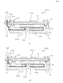
- Fig. 5 shows a circuit board 30 according to the second embodiment.
- the same numerals as in Fig. 1 are attached and the overlapping explanations are omitted.
- the circuit board 30 has approximately the same composition as the circuit board 1, but the modes of an injection molded circuit board 31 etc. differ.
- a pair of convex parts 33a and 33b is formed in the injection molded circuit board 31.
- the convex parts 33a and 33b function as the printed circuit board mounting part in the injection molded circuit board 31.
- the conductor parts 15b exposed from the injection molded circuit board 31 expose on the upper surface of the convex parts 33a and 33b.
- the printed circuit board 5 is installed so that it straddles at least a pair of convex parts 33a and 33b.
- the conductor parts 15b penetrate the through holes 21 of the printed circuit board 5 and then are electrically connected to the printed circuit board 5 by the solder parts 25.
- the female screw part 17 is provided in the convex part 33b. Therefore, the printed circuit board 5 is fixed to the injection molded circuit board 31 by the bolt 23 on the convex part 33b.
- the female screw part 17 and the conductor part 15b are exposed on the convex part 33a.
- the through hole 21 of the printed circuit board 5 is allocated on the convex part 33a. Therefore, the printed circuit board 5 is electrically connected to the conductor part 15b and also is fixed to the injection molded circuit board 31 by the bolt 23 on the convex part 33a.
- the female screw parts 17 and the conductor parts 15b may be exposed on both of the convex parts 33a and 33b. In the following explanation, the convex parts 33a and 33b together are called the convex parts 33.
- a space is formed between the printed circuit board 5 and the injection molded circuit board 31 in a region sandwiched by the convex parts 33.
- the electronic parts 13a to be mounted on the injection molded circuit board 31 may be placed in this space.
- the electronic parts mounting part 7 is formed between the convex parts 33.
- the same effect as the first embodiment can be obtained.
- a small circuit board can be obtained since the electronic parts to be mounted on the injection molded circuit board and the electronic parts to be mounted on the printed circuit board can be placed in layers.
- Fig. 6 (a) shows a circuit board 40a according to the third embodiment.
- stress relaxation parts 41 are further formed compared to the circuit board 30.
- the conductor parts 15b which are to be connected to the printed circuit board 5 do not penetrate the printed circuit board 5 straight from the surface of the resin 9.
- the conductor parts 15b are configured to project out in approximately horizontal direction (approximately parallel to the surface of the circuit board) from the side surface of an injection molded circuit board 43a and further to be bent upward. It is desirable that horizontal and vertical parts are formed at least in a section of the bent parts.
- the bent parts in the conductor parts 15b function as the stress relaxation parts 41.
- the conductor parts 15b are not restrained at the stress relaxation parts 41 and some of their sections can be deformed in accordance with the deformation due to the thermal expansion difference between the printed circuit board 5 and the injection molded circuit board 43a. Thereby, the stress relaxation parts 41 can suppress generation of stress at the solder parts 25.
- the composition of the stress relaxation part 41 is not limited to the example of Fig. 6 (a) . It is not necessary that the stress relaxation part 41 is exposed from a side surface of the injection molded circuit board 43b, as is shown in the circuit board 40b in Fig. 6 (b) , for example. Namely, the stress relaxation part 41 has only to be a section of the conductor part 15b not restrained and deformable, located between the junction with the printed circuit board 5 and the point where the conductor part 15b starts to be exposed from the surface of the injection molded circuit board.
- Fig. 7 further shows an example of modification of the stress relaxation part.
- the circuit board 50 shown in Fig. 7 has approximately the same composition as the circuit board 40a, but a small diameter part is formed instead of the bent parts in the conductor part 15b. Namely, a lower stiffness part is provided in the non-restrained part of the conductor part 15b. The lower stiffness part is more deformable than other parts. Thereby, the stress relaxation part deforms easily corresponding to the displacement between the printed circuit board and the injection molded circuit board described above, and thus the stress generated at the solder part 25 can be eased.
- the same effect as the first embodiment can be obtained. Also, since a part of the conductor part 15b which connects the printed circuit board to the injection molded circuit board is exposed from the resin of the injection molded circuit board to form the stress relaxation part, the stress generated at the solder part 25 can be eased.
- each of the compositions described above can naturally be combined with one another. Through holes do not have to be used for connection between the printed circuit board and the injection molded circuit board.
- the printed circuit board and the injection molded circuit board may be fixed using securing members such as pins which can fix them mechanically, instead of the bolts.
Landscapes
- Engineering & Computer Science (AREA)
- Microelectronics & Electronic Packaging (AREA)
- Manufacturing & Machinery (AREA)
- Structure Of Printed Boards (AREA)
- Mounting Of Printed Circuit Boards And The Like (AREA)
- Combinations Of Printed Boards (AREA)
Applications Claiming Priority (2)
| Application Number | Priority Date | Filing Date | Title |
|---|---|---|---|
| JP2011051166A JP5449237B2 (ja) | 2011-03-09 | 2011-03-09 | 基板および基板の製造方法 |
| PCT/JP2012/054711 WO2012121036A1 (ja) | 2011-03-09 | 2012-02-27 | 基板および基板の製造方法 |
Publications (2)
| Publication Number | Publication Date |
|---|---|
| EP2685795A1 true EP2685795A1 (de) | 2014-01-15 |
| EP2685795A4 EP2685795A4 (de) | 2015-03-25 |
Family
ID=46798004
Family Applications (1)
| Application Number | Title | Priority Date | Filing Date |
|---|---|---|---|
| EP12754301.5A Withdrawn EP2685795A4 (de) | 2011-03-09 | 2012-02-27 | Leiterplatte und verfahren zur herstellung einer leiterplatte |
Country Status (5)
| Country | Link |
|---|---|
| US (1) | US20140008105A1 (de) |
| EP (1) | EP2685795A4 (de) |
| JP (1) | JP5449237B2 (de) |
| CN (1) | CN103380662A (de) |
| WO (1) | WO2012121036A1 (de) |
Families Citing this family (5)
| Publication number | Priority date | Publication date | Assignee | Title |
|---|---|---|---|---|
| US10334718B2 (en) * | 2013-11-21 | 2019-06-25 | Zf Friedrichshafen Ag | Multi-functional high-current circuit board |
| CN104078211B (zh) * | 2014-06-12 | 2016-06-08 | 国网江苏省电力公司淮安供电公司 | 变压器的磁极线圈安装基板结构 |
| CN104078210B (zh) * | 2014-06-12 | 2016-06-08 | 国网江苏省电力公司淮安供电公司 | 安装基板固定磁极线圈的方法 |
| CN106028649B (zh) * | 2016-07-28 | 2019-02-12 | Oppo广东移动通信有限公司 | 移动终端的电路板和具有其的移动终端 |
| KR102554299B1 (ko) * | 2016-10-07 | 2023-07-12 | 한국전력공사 | 매립형 3차원 구조 전자회로 부품 및 그 제조방법 |
Family Cites Families (21)
| Publication number | Priority date | Publication date | Assignee | Title |
|---|---|---|---|---|
| US4630174A (en) * | 1983-10-31 | 1986-12-16 | Kaufman Lance R | Circuit package with external circuit board and connection |
| JPH0312233U (de) * | 1989-06-20 | 1991-02-07 | ||
| JPH0334703A (ja) * | 1989-06-30 | 1991-02-14 | Nec Corp | 基板間のパターン接続器 |
| JPH066529Y2 (ja) * | 1990-02-02 | 1994-02-16 | 守 水沢 | 制御盤用プリント板 |
| JPH06275328A (ja) * | 1993-03-19 | 1994-09-30 | Fuji Elelctrochem Co Ltd | プリント基板用リード端子とその実装方法 |
| JPH0846317A (ja) * | 1994-07-26 | 1996-02-16 | Honda Motor Co Ltd | 制御基板 |
| JPH0936513A (ja) * | 1995-07-20 | 1997-02-07 | Japan Aviation Electron Ind Ltd | プリント回路装置 |
| JPH09121079A (ja) * | 1995-10-26 | 1997-05-06 | Fujitsu Ten Ltd | 複合基板構造 |
| JPH10290054A (ja) * | 1997-04-16 | 1998-10-27 | Sony Corp | プリント配線基板 |
| JPH11225459A (ja) * | 1998-02-05 | 1999-08-17 | Matsushita Electric Ind Co Ltd | モータ制御装置 |
| JP2000133897A (ja) * | 1998-10-27 | 2000-05-12 | Matsushita Electric Ind Co Ltd | 樹脂成形基板 |
| JP3538045B2 (ja) * | 1998-12-09 | 2004-06-14 | 三菱電機株式会社 | Rf回路モジュール |
| GB9911905D0 (en) * | 1999-05-22 | 1999-07-21 | Trw Lucas Varity Electric | Improvement relating to electrical power assisted steering |
| JP4510975B2 (ja) * | 2000-02-08 | 2010-07-28 | パナソニック株式会社 | 回路基板 |
| JP4026044B2 (ja) * | 2000-05-09 | 2007-12-26 | 株式会社デンソー | 基板接続部材 |
| JP4551552B2 (ja) | 2000-10-24 | 2010-09-29 | 米沢電線株式会社 | 複合回路基板 |
| JP2002368017A (ja) * | 2001-06-05 | 2002-12-20 | Nikon Corp | 実装基板 |
| JP4193650B2 (ja) * | 2003-09-18 | 2008-12-10 | 株式会社デンソー | 回路基板 |
| JP2009094457A (ja) * | 2007-09-18 | 2009-04-30 | Olympus Corp | 積層実装構造体及び積層実装構造体の製造方法 |
| US7800222B2 (en) * | 2007-11-29 | 2010-09-21 | Infineon Technologies Ag | Semiconductor module with switching components and driver electronics |
| CN101681907B (zh) * | 2007-11-30 | 2012-11-07 | 松下电器产业株式会社 | 散热结构体基板和使用其的模块及散热结构体基板的制造方法 |
-
2011
- 2011-03-09 JP JP2011051166A patent/JP5449237B2/ja active Active
-
2012
- 2012-02-27 CN CN2012800085530A patent/CN103380662A/zh active Pending
- 2012-02-27 EP EP12754301.5A patent/EP2685795A4/de not_active Withdrawn
- 2012-02-27 WO PCT/JP2012/054711 patent/WO2012121036A1/ja not_active Ceased
-
2013
- 2013-09-09 US US14/021,053 patent/US20140008105A1/en not_active Abandoned
Also Published As
| Publication number | Publication date |
|---|---|
| WO2012121036A1 (ja) | 2012-09-13 |
| JP2012190883A (ja) | 2012-10-04 |
| EP2685795A4 (de) | 2015-03-25 |
| CN103380662A (zh) | 2013-10-30 |
| JP5449237B2 (ja) | 2014-03-19 |
| US20140008105A1 (en) | 2014-01-09 |
Similar Documents
| Publication | Publication Date | Title |
|---|---|---|
| US10576912B2 (en) | Circuit assembly and electrical junction box | |
| US8436459B2 (en) | Power semiconductor module | |
| US10038315B2 (en) | Circuit assembly and electrical junction box | |
| US6791170B1 (en) | Onboard semiconductor device | |
| CN104620377B (zh) | 半导体装置 | |
| US10517181B2 (en) | Electronic control device and manufacturing method for same | |
| US11545770B2 (en) | Electric-power conversion apparatus | |
| US20140008105A1 (en) | Circuit board and method for manufacturing circuit board | |
| WO2011129130A1 (ja) | 基板および基板の製造方法 | |
| JP5697020B2 (ja) | 基板および基板の製造方法 | |
| US8091218B2 (en) | Method of manufacturing a rigid printed wiring board | |
| WO2011086768A1 (ja) | 基板および基板の製造方法 | |
| EP4050787B1 (de) | Stromwandler | |
| US20130044447A1 (en) | Vehicle-mountable junction box, and circuit member and circuit unit usable for the vehicle-mountable junction box | |
| US20210084765A1 (en) | Method for Mechanically Connecting and Arranging Electronic Components | |
| JP2014096260A (ja) | フラット配線材及びそれを用いた実装体 | |
| WO2012099101A1 (ja) | 基板間接続端子およびそれを用いたインバータ、電動圧縮機 | |
| CN114122769B (zh) | 电力转换装置和零部件间连接构造 | |
| JP5415858B2 (ja) | 厚導体基板及びその製造方法 | |
| JP5255592B2 (ja) | 基板 | |
| JP4914247B2 (ja) | 電子制御装置 | |
| US20240268024A1 (en) | Solder mounting land and charger | |
| CN112910285B (zh) | 一种逆变器电力系统及其制造方法 | |
| JP4297318B2 (ja) | 回路基板および電気接続箱 | |
| JP2007267596A (ja) | 電気接続箱 |
Legal Events
| Date | Code | Title | Description |
|---|---|---|---|
| PUAI | Public reference made under article 153(3) epc to a published international application that has entered the european phase |
Free format text: ORIGINAL CODE: 0009012 |
|
| 17P | Request for examination filed |
Effective date: 20130828 |
|
| AK | Designated contracting states |
Kind code of ref document: A1 Designated state(s): AL AT BE BG CH CY CZ DE DK EE ES FI FR GB GR HR HU IE IS IT LI LT LU LV MC MK MT NL NO PL PT RO RS SE SI SK SM TR |
|
| DAX | Request for extension of the european patent (deleted) | ||
| A4 | Supplementary search report drawn up and despatched |
Effective date: 20150224 |
|
| RIC1 | Information provided on ipc code assigned before grant |
Ipc: H05K 3/40 20060101ALI20150218BHEP Ipc: H05K 3/00 20060101ALI20150218BHEP Ipc: H05K 1/14 20060101AFI20150218BHEP Ipc: H05K 1/02 20060101ALI20150218BHEP |
|
| STAA | Information on the status of an ep patent application or granted ep patent |
Free format text: STATUS: THE APPLICATION HAS BEEN WITHDRAWN |
|
| 18W | Application withdrawn |
Effective date: 20150601 |