EP2688093A1 - Verfahren und Vorrichtung zur Selbstmontage von Komponenten auf einem Substrat - Google Patents
Verfahren und Vorrichtung zur Selbstmontage von Komponenten auf einem Substrat Download PDFInfo
- Publication number
- EP2688093A1 EP2688093A1 EP12177060.6A EP12177060A EP2688093A1 EP 2688093 A1 EP2688093 A1 EP 2688093A1 EP 12177060 A EP12177060 A EP 12177060A EP 2688093 A1 EP2688093 A1 EP 2688093A1
- Authority
- EP
- European Patent Office
- Prior art keywords
- components
- solder
- substrate
- self
- assembly
- Prior art date
- Legal status (The legal status is an assumption and is not a legal conclusion. Google has not performed a legal analysis and makes no representation as to the accuracy of the status listed.)
- Granted
Links
Images


Classifications
-
- H—ELECTRICITY
- H10—SEMICONDUCTOR DEVICES; ELECTRIC SOLID-STATE DEVICES NOT OTHERWISE PROVIDED FOR
- H10W—GENERIC PACKAGES, INTERCONNECTIONS, CONNECTORS OR OTHER CONSTRUCTIONAL DETAILS OF DEVICES COVERED BY CLASS H10
- H10W90/00—Package configurations
-
- B—PERFORMING OPERATIONS; TRANSPORTING
- B23—MACHINE TOOLS; METAL-WORKING NOT OTHERWISE PROVIDED FOR
- B23K—SOLDERING OR UNSOLDERING; WELDING; CLADDING OR PLATING BY SOLDERING OR WELDING; CUTTING BY APPLYING HEAT LOCALLY, e.g. FLAME CUTTING; WORKING BY LASER BEAM
- B23K1/00—Soldering, e.g. brazing, or unsoldering
- B23K1/0008—Soldering, e.g. brazing, or unsoldering specially adapted for particular articles or work
- B23K1/0016—Soldering of electronic components
-
- B—PERFORMING OPERATIONS; TRANSPORTING
- B23—MACHINE TOOLS; METAL-WORKING NOT OTHERWISE PROVIDED FOR
- B23K—SOLDERING OR UNSOLDERING; WELDING; CLADDING OR PLATING BY SOLDERING OR WELDING; CUTTING BY APPLYING HEAT LOCALLY, e.g. FLAME CUTTING; WORKING BY LASER BEAM
- B23K1/00—Soldering, e.g. brazing, or unsoldering
- B23K1/20—Preliminary treatment of work or areas to be soldered, e.g. in respect of a galvanic coating
-
- B—PERFORMING OPERATIONS; TRANSPORTING
- B23—MACHINE TOOLS; METAL-WORKING NOT OTHERWISE PROVIDED FOR
- B23K—SOLDERING OR UNSOLDERING; WELDING; CLADDING OR PLATING BY SOLDERING OR WELDING; CUTTING BY APPLYING HEAT LOCALLY, e.g. FLAME CUTTING; WORKING BY LASER BEAM
- B23K35/00—Rods, electrodes, materials, or media, for use in soldering, welding, or cutting
- B23K35/02—Rods, electrodes, materials, or media, for use in soldering, welding, or cutting characterised by mechanical features, e.g. shape
- B23K35/0222—Rods, electrodes, materials, or media, for use in soldering, welding, or cutting characterised by mechanical features, e.g. shape for use in soldering or brazing
- B23K35/0233—Sheets or foils
- B23K35/0238—Sheets or foils layered
-
- B—PERFORMING OPERATIONS; TRANSPORTING
- B23—MACHINE TOOLS; METAL-WORKING NOT OTHERWISE PROVIDED FOR
- B23K—SOLDERING OR UNSOLDERING; WELDING; CLADDING OR PLATING BY SOLDERING OR WELDING; CUTTING BY APPLYING HEAT LOCALLY, e.g. FLAME CUTTING; WORKING BY LASER BEAM
- B23K35/00—Rods, electrodes, materials, or media, for use in soldering, welding, or cutting
- B23K35/02—Rods, electrodes, materials, or media, for use in soldering, welding, or cutting characterised by mechanical features, e.g. shape
- B23K35/0222—Rods, electrodes, materials, or media, for use in soldering, welding, or cutting characterised by mechanical features, e.g. shape for use in soldering or brazing
- B23K35/0244—Powders, particles or spheres; Preforms made therefrom
- B23K35/025—Pastes, creams or slurries
-
- B—PERFORMING OPERATIONS; TRANSPORTING
- B23—MACHINE TOOLS; METAL-WORKING NOT OTHERWISE PROVIDED FOR
- B23K—SOLDERING OR UNSOLDERING; WELDING; CLADDING OR PLATING BY SOLDERING OR WELDING; CUTTING BY APPLYING HEAT LOCALLY, e.g. FLAME CUTTING; WORKING BY LASER BEAM
- B23K35/00—Rods, electrodes, materials, or media, for use in soldering, welding, or cutting
- B23K35/22—Rods, electrodes, materials, or media, for use in soldering, welding, or cutting characterised by the composition or nature of the material
- B23K35/24—Selection of soldering or welding materials proper
- B23K35/26—Selection of soldering or welding materials proper with the principal constituent melting at less than 400°C
- B23K35/262—Sn as the principal constituent
-
- B—PERFORMING OPERATIONS; TRANSPORTING
- B23—MACHINE TOOLS; METAL-WORKING NOT OTHERWISE PROVIDED FOR
- B23K—SOLDERING OR UNSOLDERING; WELDING; CLADDING OR PLATING BY SOLDERING OR WELDING; CUTTING BY APPLYING HEAT LOCALLY, e.g. FLAME CUTTING; WORKING BY LASER BEAM
- B23K35/00—Rods, electrodes, materials, or media, for use in soldering, welding, or cutting
- B23K35/22—Rods, electrodes, materials, or media, for use in soldering, welding, or cutting characterised by the composition or nature of the material
- B23K35/24—Selection of soldering or welding materials proper
- B23K35/26—Selection of soldering or welding materials proper with the principal constituent melting at less than 400°C
- B23K35/264—Bi as the principal constituent
-
- B—PERFORMING OPERATIONS; TRANSPORTING
- B23—MACHINE TOOLS; METAL-WORKING NOT OTHERWISE PROVIDED FOR
- B23K—SOLDERING OR UNSOLDERING; WELDING; CLADDING OR PLATING BY SOLDERING OR WELDING; CUTTING BY APPLYING HEAT LOCALLY, e.g. FLAME CUTTING; WORKING BY LASER BEAM
- B23K35/00—Rods, electrodes, materials, or media, for use in soldering, welding, or cutting
- B23K35/22—Rods, electrodes, materials, or media, for use in soldering, welding, or cutting characterised by the composition or nature of the material
- B23K35/24—Selection of soldering or welding materials proper
- B23K35/26—Selection of soldering or welding materials proper with the principal constituent melting at less than 400°C
- B23K35/268—Pb as the principal constituent
-
- H—ELECTRICITY
- H10—SEMICONDUCTOR DEVICES; ELECTRIC SOLID-STATE DEVICES NOT OTHERWISE PROVIDED FOR
- H10W—GENERIC PACKAGES, INTERCONNECTIONS, CONNECTORS OR OTHER CONSTRUCTIONAL DETAILS OF DEVICES COVERED BY CLASS H10
- H10W72/00—Interconnections or connectors in packages
- H10W72/01—Manufacture or treatment
- H10W72/016—Manufacture or treatment of strap connectors
-
- H—ELECTRICITY
- H10—SEMICONDUCTOR DEVICES; ELECTRIC SOLID-STATE DEVICES NOT OTHERWISE PROVIDED FOR
- H10W—GENERIC PACKAGES, INTERCONNECTIONS, CONNECTORS OR OTHER CONSTRUCTIONAL DETAILS OF DEVICES COVERED BY CLASS H10
- H10W72/00—Interconnections or connectors in packages
- H10W72/01—Manufacture or treatment
- H10W72/0198—Manufacture or treatment batch processes
-
- H—ELECTRICITY
- H10—SEMICONDUCTOR DEVICES; ELECTRIC SOLID-STATE DEVICES NOT OTHERWISE PROVIDED FOR
- H10W—GENERIC PACKAGES, INTERCONNECTIONS, CONNECTORS OR OTHER CONSTRUCTIONAL DETAILS OF DEVICES COVERED BY CLASS H10
- H10W72/00—Interconnections or connectors in packages
- H10W72/071—Connecting or disconnecting
- H10W72/0711—Apparatus therefor
- H10W72/07173—Means for moving chips, wafers or other parts, e.g. conveyor belts
-
- H—ELECTRICITY
- H10—SEMICONDUCTOR DEVICES; ELECTRIC SOLID-STATE DEVICES NOT OTHERWISE PROVIDED FOR
- H10W—GENERIC PACKAGES, INTERCONNECTIONS, CONNECTORS OR OTHER CONSTRUCTIONAL DETAILS OF DEVICES COVERED BY CLASS H10
- H10W72/00—Interconnections or connectors in packages
- H10W72/071—Connecting or disconnecting
- H10W72/072—Connecting or disconnecting of bump connectors
- H10W72/07221—Aligning
- H10W72/07227—Aligning involving guiding structures, e.g. spacers or supporting members
-
- H—ELECTRICITY
- H10—SEMICONDUCTOR DEVICES; ELECTRIC SOLID-STATE DEVICES NOT OTHERWISE PROVIDED FOR
- H10W—GENERIC PACKAGES, INTERCONNECTIONS, CONNECTORS OR OTHER CONSTRUCTIONAL DETAILS OF DEVICES COVERED BY CLASS H10
- H10W72/00—Interconnections or connectors in packages
- H10W72/071—Connecting or disconnecting
- H10W72/072—Connecting or disconnecting of bump connectors
- H10W72/07231—Techniques
- H10W72/07236—Soldering or alloying
-
- H—ELECTRICITY
- H10—SEMICONDUCTOR DEVICES; ELECTRIC SOLID-STATE DEVICES NOT OTHERWISE PROVIDED FOR
- H10W—GENERIC PACKAGES, INTERCONNECTIONS, CONNECTORS OR OTHER CONSTRUCTIONAL DETAILS OF DEVICES COVERED BY CLASS H10
- H10W72/00—Interconnections or connectors in packages
- H10W72/071—Connecting or disconnecting
- H10W72/073—Connecting or disconnecting of die-attach connectors
- H10W72/07321—Aligning
-
- H—ELECTRICITY
- H10—SEMICONDUCTOR DEVICES; ELECTRIC SOLID-STATE DEVICES NOT OTHERWISE PROVIDED FOR
- H10W—GENERIC PACKAGES, INTERCONNECTIONS, CONNECTORS OR OTHER CONSTRUCTIONAL DETAILS OF DEVICES COVERED BY CLASS H10
- H10W72/00—Interconnections or connectors in packages
- H10W72/071—Connecting or disconnecting
- H10W72/073—Connecting or disconnecting of die-attach connectors
- H10W72/07331—Connecting techniques
- H10W72/07336—Soldering or alloying
-
- H—ELECTRICITY
- H10—SEMICONDUCTOR DEVICES; ELECTRIC SOLID-STATE DEVICES NOT OTHERWISE PROVIDED FOR
- H10W—GENERIC PACKAGES, INTERCONNECTIONS, CONNECTORS OR OTHER CONSTRUCTIONAL DETAILS OF DEVICES COVERED BY CLASS H10
- H10W72/00—Interconnections or connectors in packages
- H10W72/071—Connecting or disconnecting
- H10W72/073—Connecting or disconnecting of die-attach connectors
- H10W72/07341—Controlling the bonding environment, e.g. atmosphere composition or temperature
-
- H—ELECTRICITY
- H10—SEMICONDUCTOR DEVICES; ELECTRIC SOLID-STATE DEVICES NOT OTHERWISE PROVIDED FOR
- H10W—GENERIC PACKAGES, INTERCONNECTIONS, CONNECTORS OR OTHER CONSTRUCTIONAL DETAILS OF DEVICES COVERED BY CLASS H10
- H10W72/00—Interconnections or connectors in packages
- H10W72/20—Bump connectors, e.g. solder bumps or copper pillars; Dummy bumps; Thermal bumps
- H10W72/221—Structures or relative sizes
- H10W72/222—Multilayered bumps, e.g. a coating on top and side surfaces of a bump core
-
- H—ELECTRICITY
- H10—SEMICONDUCTOR DEVICES; ELECTRIC SOLID-STATE DEVICES NOT OTHERWISE PROVIDED FOR
- H10W—GENERIC PACKAGES, INTERCONNECTIONS, CONNECTORS OR OTHER CONSTRUCTIONAL DETAILS OF DEVICES COVERED BY CLASS H10
- H10W72/00—Interconnections or connectors in packages
- H10W72/20—Bump connectors, e.g. solder bumps or copper pillars; Dummy bumps; Thermal bumps
- H10W72/241—Dispositions, e.g. layouts
-
- H—ELECTRICITY
- H10—SEMICONDUCTOR DEVICES; ELECTRIC SOLID-STATE DEVICES NOT OTHERWISE PROVIDED FOR
- H10W—GENERIC PACKAGES, INTERCONNECTIONS, CONNECTORS OR OTHER CONSTRUCTIONAL DETAILS OF DEVICES COVERED BY CLASS H10
- H10W72/00—Interconnections or connectors in packages
- H10W72/20—Bump connectors, e.g. solder bumps or copper pillars; Dummy bumps; Thermal bumps
- H10W72/251—Materials
- H10W72/252—Materials comprising solid metals or solid metalloids, e.g. PbSn, Ag or Cu
-
- H—ELECTRICITY
- H10—SEMICONDUCTOR DEVICES; ELECTRIC SOLID-STATE DEVICES NOT OTHERWISE PROVIDED FOR
- H10W—GENERIC PACKAGES, INTERCONNECTIONS, CONNECTORS OR OTHER CONSTRUCTIONAL DETAILS OF DEVICES COVERED BY CLASS H10
- H10W72/00—Interconnections or connectors in packages
- H10W72/30—Die-attach connectors
- H10W72/321—Structures or relative sizes of die-attach connectors
- H10W72/322—Multilayered die-attach connectors, e.g. a coating on a top surface of a core
-
- H—ELECTRICITY
- H10—SEMICONDUCTOR DEVICES; ELECTRIC SOLID-STATE DEVICES NOT OTHERWISE PROVIDED FOR
- H10W—GENERIC PACKAGES, INTERCONNECTIONS, CONNECTORS OR OTHER CONSTRUCTIONAL DETAILS OF DEVICES COVERED BY CLASS H10
- H10W72/00—Interconnections or connectors in packages
- H10W72/30—Die-attach connectors
- H10W72/351—Materials of die-attach connectors
- H10W72/352—Materials of die-attach connectors comprising metals or metalloids, e.g. solders
-
- H—ELECTRICITY
- H10—SEMICONDUCTOR DEVICES; ELECTRIC SOLID-STATE DEVICES NOT OTHERWISE PROVIDED FOR
- H10W—GENERIC PACKAGES, INTERCONNECTIONS, CONNECTORS OR OTHER CONSTRUCTIONAL DETAILS OF DEVICES COVERED BY CLASS H10
- H10W99/00—Subject matter not provided for in other groups of this subclass
Definitions
- the invention relates to a method of self-assembly including self-alignment of components on a substrate on the basis of surface tension of liquid solder for applications that require reliable operation of the self-assembled objects at elevated operation temperatures. It also relates to a method and an apparatus of fluidic self-assembly of a plurality of components onto receptor sites on the surface of a substrate, where each receptor site is formed of a selective adhesive which adheres to at least a part of the components resulting in the capture, self-alignment and/or attachment of the components at the receptor sites, integrating component delivery, removal, and attachment over increasingly large surfaces.
- the process has the advantage that it produces a flat surface. Assembled components fill the wells and form a flush surface. Subsequent components slide over already assembled objects and there is little interference.
- This particular process has the advantage the self-assembled objects are not protruding. Scaling to large areas and continuous assembly on webs having widths of more than 10 cm has been possible with little effort in terms of the machine design.
- This process requires very specific die geometries ⁇ L or T shaped blocks for angular orientation and trapezoids to prevent up-side down assembly ⁇ these particular shapes are not common in the microelectronics industry; most dies are square in shape. While they remain valid solutions they limit wide spread use. Attempts of adoption by other manufacturers remain critically low because of the required use of trapezoidal chips that are not widely used. A more universal solution is desired and would increase the chance of technology adoption and transition.
- An advantage of all self-assembly processes is that they are massively parallel, which potentially reduces the assembly costs dramatically relative to the costs of traditional deterministic pick and place methods that use serial robotic methods.
- solder directed self-assembly is for example described and applied in US 7,774,929 .
- the components self-assemble and attach to the solder-coated areas due to the reduction of the surface free energy of the liquid solder surface.
- the method has been applied to direct the assembly of chip-sized components onto surfaces from a heated suspension primarily in the context of solid state lighting, photovoltaic, and multicomponent sensors.
- One of the mechanisms of self-assembly and attachment of the chips is based on surface tension directed self-assembly on the basis of liquid solder.
- the self-assembly process is driven by the minimization of surface free energy of the liquid solder.
- the metal contact on the component binds to the liquid-solder-based-receptors during the self-assembly process at a temperature where the solder is molten.
- the solder wets the metal contact during the process and the minimization of the free surface area of the liquid solder drives the assembly into a stable, aligned position.
- the parallel assembly of large number of components has been accomplished using this process.
- liquid-solder-coated areas act as receptors for subunits during the assembly ⁇ no manipulator is needed ⁇ , they form rigid bonds upon solidification ⁇ no adhesive is needed ⁇ , and provide electrical input/output-connectors to operate the final device ⁇ no wire bonder is needed.
- Solder directed fluidic self-assembly as it has been described today is done inside a closed vial, barrel, or container to suspend the self-assembly components in a fluid at a temperature where the solder is molten.
- solder directed self-assembly As it is known today is the fact that the melting point of the solder has to be below the boiling point of the fluid that is used in the fluidic self-assembly process. For example often water is used as a fluid which limits the melting point of the solder to be below 100°C. To assemble devices then mostly solder is used that has a melting point below 60°C. While it is possible to replace the water with ethylene glycol or other higher boiling point liquids, it has not yet been possible to form reliable interconnects using this approach. It appears that there are no solvents that support the self-assembly at sufficiently high temperatures that would work with the same solder based interconnects that are used in the electronics industry. This is the main reason why solder directed self-assembly has not been used in an industrial process today.
- solder stack is composed of two solder layers that have different compositions and thus different melting points.
- the objects are always brought into contact using micromanipulators, referred to as deterministic rather than stochastic assembly.
- TW 517370 B for example the stack is used to avoid bridging between pads and to increase the bump height as well as to better control the bump dimensions.
- solder balls are disclosed that have high melting point cores which are partially or completely coated with a lower melting point solder.
- the balls are applied in a ball grid array (BGA) and the particular process allows for a tighter control of the ball dimensions which in turn allows for higher interconnect density in surface mount packaging without bridging.
- BGA ball grid array
- the first document describes the use of a slurry of components that slides across a planar surface. The components drop into the recessed openings on the basis of gravity and shape recognition.
- the second document describes the use of a closed rotating barrel that holds the self-assembly substrate. The substrate is attached inside the barrel and points towards the center of the barrel. The barrel itself holds the self-assembly objects. Back-and-forth partial rotation of the barrel leads to a successive sweeping motion of self-assembly components that slide over the surface and that interact with the receptors.
- First object of the invention is to enhance a self-assembly method based on solder in a way that also microelectronic components which have to withstand higher temperatures than currently achievable can be produced by using a self-assembly process as described in the beginning.
- Another object of the invention is to enhance a method of and to develop an apparatus for self-assembly of a plurality of components onto receptor sites on a surface of a substrate where the receptor sites are formed of selective adhesives and in particular to reduce shear forces caused by protruding elements to a minimum to allow the assembly of larger numbers of protruding components than currently possible.
- self-assembly of large numbers of protruding components over wide areas substrates forming reliable interconnects should be achieved.
- the first problem is solved by a method as described in claim 1.
- the second problem is solved by a method as described in claim 6 and an apparatus as described in claim 12.
- Preferred and advantageous embodiments of the methods and the apparatus are described in the dependent claims.
- Figure 1 shows the basic concept of a method of self-assembly including self-alignment of components 1 on a substrate 2 on the basis of surface tension of liquid solder.
- the method involves a solder stack composed of an outermost layer of solder 3 on top and at least another layer of solder 4, the layers of solder having successively increasing melting points from top to bottom.
- the method comprises the following steps: In a first step the solder stack is heated to a temperature between the melting point of the outermost layer of solder 3 and the at least another layer of solder 4. This corresponds to the situation shown in figure 1 in the upper left corner.
- the outermost layer 3 is molten; due to the surface tension the molten solder has a convex shape on its surface towards its environment since it tries to minimize its surface free energy.
- the molten outermost layer 3 is then used to form a receptor which adheres to the components 1 as shown in the upper right corner of figure 1 . Since the molten solder tends to minimize its surface, when a component 1 is adhered to the solder, this will result in the self-assembly, self-alignment and attachment of the components 1.
- Melting of solder is achieved in a liquid environment, the liquid being heated but having a boiling point well above the melting point of the solder used in the outermost layer 3.
- the components 1 therefore are dispensed in a first fluid 6 which is also shown in the first three steps displayed in figure 1 .
- the first fluid 6 is being heated to a temperature below its boiling point but above the melting point of the outermost layer of solder 3.
- This layer of solder 3 then forms a selective adhesive to capture the components 1 as shown in the upper right corner of figure 1 .
- this step can for example be performed in a second fluid at a temperature above the boiling point of the first fluid, or in a gaseous environment like nitrogen or argon, as shown in figure 1 .
- This method overcomes the problem of prior solder directed self-assembly processes that used a single solder layer leading to an interconnect that had a melting point that was limited to be smaller than the boiling point of the first fluid 6 and where no reliable interconnects could be made which would withstand the higher operating temperatures of the assembled devices as they often occur in microdevices. It describes a two-face solder-based receptor to enable high temperature operation of self-assembled objects. However, this aspect is limited to the field of surface tension directed self-assembly on the basis of liquid solder. It extends the allowed operating temperature of current assemblies produced using prior art in the field of solder directed self-assembly which is somewhere in the range of 40-100°C to well above 200°C.
- the new kind of solder based receptor is composed of at least two different solder layers.
- the outermost layer of solder 3 is composed of a low melting point metal alloy and the at least another layer of solder 4 is composed of a higher melting point metal alloy.
- the first step is carried out at low temperature where the low melting point section of the receptor is molten.
- Examples for low melting point alloys are various combinations of the element In, Bi, Sn, Zn, Cd, and Pb in different combination and ratios.
- RoHS Hazardous Substances Directive
- lead and cadmium free solder alloys are also available.
- Different melting points of the solder can be realised using different alloys, for instance a melting point (MP) of 29.8° using 100% Ga, a MP of 47°C using an alloy of ⁇ 44.7%Bi, 22.6% Pb, 19.1% In, 8.3% Sn, 5.3 % Cd ⁇ , a MP of 58°C using ⁇ 49% Bi, 18% Pb, 12% Sn, 21% In ⁇ , a MP of 60°C using ⁇ 51% In 32.5% Bi 16.5% Sn ⁇ , a MP of 69°C using ⁇ 49% Bi, 18% Pb, 18% In, 15% Sn ⁇ , a MP of 79°C using ⁇ 57% Bi, 26% In, 17% Sn ⁇ , a MP of 72 °C using ⁇ 66.3% In, 33.7% Bi ⁇ , a MP of 79°C using ⁇ 57% Bi, 26% In, 17% Sn ⁇ , a MP of 95°C using ⁇ 52.5% Bi, 32% Pb, 15.5% Sn
- the first self-assembly step can and should therefore still be performed in a liquid environment at a modest temperature.
- the first fluid 6 can be water, ethylene glycol or oil.
- the second self-assembly step is a higher temperature reflow step which can be performed in a liquid having a higher boiling point than the first fluid, for example various oil, or inorganic and organic solvents can be used. It also can be performed in a gaseous environment like in air, nitrogen or argon. The temperature is raised to reflow both layers. The reflow step completes the self-assembly and final self-alignment while producing a reliable interconnect with increased melting point.
- the higher melting point solder layer can therefore be composed of a large variety of metallic alloys commonly also used in the electronics industry. Examples include alloys composed of Sn, Ag, Cu in different compositions (so-called SAC solder alloys), and Au.
- an alloy composed of 93.6% Sn, 4.7% Ag, and 1.7% Cu has a melting point of 217°C
- a metal alloy composed of 80% Au, and 20% Sn has a melting point of 280°C.
- solder paste SAC305 composed of 96.5% Sn, 3.0% Ag, and 0.5% Cu is used.
- the previously mentioned materials are only a few examples.
- the industry uses at least 40 different solder compositions and the list of possible combinations is extensive. While figure 1 shows similar thickness for the two solder layers 3 and 4, it is clear that the thickness of the respective layers can be adjusted to tune the melting point and composition of the mixed phase that is formed after reflow.
- the thickness of the at least another layer of solder 4 should be higher than that of the outermost layer of solder 3.
- the composition of the final solder can be tuned to achieve a desired melting point or physical property by selecting a composition of the first solder and thickness and a composition of the second solder and thickness.
- This new type of self-assembly process allows to use a solder stack to form reliable and resilient electrical or mechanical connections, either single or multiple, between the components 1 and the substrate 2, the components 1 being for example semiconductor chips, dies, LED for solid state lighting, RFID-tags, and/or even mechanical parts.
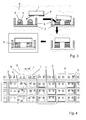
- the substrate 2 has multiple receptor sites mounted on a conveyor belt.
- An example is shown in figure 2 , with a substrate 2 on a conveyor belt 7 moving from left to right through the respective temperature regions. Displayed are four zones, marked by the small curved double lines dividing the conveyor belt 7 and the substrate 2, respectively, in different regions.
- the first region on the left is used to melt the outermost layer of solder 3 which drives the self-assembly of the components 1 into a stable and self-aligned position in the next region. This step takes place in the first fluid 6, while the outermost layer of solder 3 is molten before entering the first fluid 6.
- the components 1 When the components 1 are self-aligned and fixed at their positions, they enter a third region where they can be inspected for example, either manually or by an automatic process using image processing, the latter being the process of choice since the solder stack is repeatedly arranged over an extended surface area and comprises a large number of receptor sites.
- the next step shown in a fourth region on the right side of figure 2 corresponds to the high temperature reflow step of the entire solder stack to form an interconnecting alloy with sufficiently high melting point to ensure operation in real world electronic applications.
- the substrate 2 can also be mounted on a web; it is also possible that the web itself forms the substrate 2.
- pedestals 8 are used on the substrate 2 in combination with the solder stack to define docking sites to assemble components 1 onto the surface of the substrate 2 with unique angular rotation and/or contact pad registration.
- the components 1 displayed in figure 3 have two metal contacts 9, they therefore have to be aligned with correct orientation on the substrate to ensure their function.
- pedestals 8 are used which divide the substrate into different regions. This embodiment is in particular advantageous when used together with a conveyor belt 7 as shown in figure 4 , or webs.
- the components 1 are displayed in a transparent manner to make to contact pads on the surface of the substrate 2 and on the components 1 visible. The process easily can be extended to more than two connections.
- Another aspect is related to avoiding shear forces as they occur in self-assembly methods according to the state of the art as described for example in US 5,545,291 and US 7,774,929 and mentioned in detail in the beginning.
- Scaling the self-assembly mechanism to larger areas is more challenging in the case where protruding objects have to be assembled, since the protruding objects are exposed to additional shear forces.
- protruding objects interfere with the component delivery mechanism which has been done using a slurry of self-assembly components that slides a long the surface to populate receptor sites.
- a large number of components 1 with metal contacts 9 is shown in a liquid environment 10 as they slide along an inclined surface of a substrate 2.
- receptor sites 11 are arranged on the substrate 2. Due to the large number of components, on some of the components already adhered to the selective adhesive element, massive shear forces are exerted as demonstrated at shear points 12, resulting in a lateral shift of already assembled components 1 which might in the worst case lead to removal of those components 1 or in an alignment which is not correct.
- This difficulty can be overcome applying a fluidic self-assembly method of a plurality of components 1 onto receptor sites 11 on the surface of a substrate 2, where each receptor site 11 is formed of a selective adhesive which adheres to at least a part of the components 1 resulting in the capture, self-alignment and/or attachment of the components 1 at the receptor sites 11.
- the selective adhesive element might be a simple solder junction, a simple hydrophobic adhesive or also a solder stack, to list only a few examples.
- the substrate 2 with the receptor site 11 is transported in an essentially upright position at a predetermined speed into a delivery zone, the zone comprising a fluid 13.
- the speed may be chosen in a range between 1 cm/min and 100cm/min, but eventually larger speed can be applied as technology advances.
- the components 1 are dispensed into the fluid 13 by a dispensing unit located above the delivery zone, resulting in a portion of components 1 getting attached to receptor sites 11 and a remaining portion of components 1 forming excess components not attached to receptor sites 11.
- "Essentially upright" means that in the delivery zone the substrate and the receptor site 11 on it are aligned to a horizontal plane in a way that components 1 getting adhered will not slide down due to gravity.
- the expression "essentially upright” therefore also includes planes with an inclination angle where this condition is fulfilled.
- the inclination angle depends on the liquid and on the density of the components; it might for example take values in a range up to 55° for slow moving substrates and up to 75° in cases where the substrate velocity is increased.
- the substrate 2 is transported out of the delivery zone and rotated into a position where the receptor sites 11 take an essentially upside-down position, thereby forcing excess components stuck at the surface of the substrate 2 to drop off it and to sink to a lower region.
- the expression "essentially upside-down” includes a large variety of angles of inclination apart from the horizontal plane at which excess components drop off the substrate 2.
- the inclination angle might be ⁇ 45° for example.
- Excess components are collected at at least one collecting point at the bottom of the lower region and transported back to the dispensing unit through at least one pathway. Then they are reused.
- Speed and optionally the angle of inclination are adjusted dependent on the properties of the fluid 13 and of the components 1 to minimize the force exerted by excess components onto already assembled components 1.
- the substrate might be vibrated or a liquid jet might be directed onto the surface of the substrate 2, using the fluid 13. Vibration and jet can also be applied together.
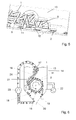
- Figure 6 shows the basic concept of an apparatus which can be used for performing the method described above, i.e. for self-assembly of components 1 onto receptor sites 11 of the surface of a substrate 2, where each receptor site 11 is formed of a selective adhesive element which adheres to at least a part of the components 1 resulting in the capture, self-assembly, self-alignment and/or attachment of the components 1 at the receptor sites 11.
- the apparatus shown in figure 1 comprises a basin 14 containing a fluid 13.
- the apparatus further comprises first transporting means for transporting the substrate 2 with the receptor sites 11 in an essential upright position at a predetermined speed and/or angle of inclination into and out of a delivery zone 16 in the fluid 13.
- a dispensing unit 17 is located which is used for dispensing components 1 into the fluid 13 and onto the substrate 2.
- the apparatus further comprises rotating means for rotating the substrate 2 into a position where the receptor sites 11 take an essentially upside-down position.
- the apparatus also comprises collecting means for collecting excess components 18 not attached to receptor sites 11 at the bottom of the basin 14, and second transporting means for returning excess components 18 to the dispensing unit 17.
- the first transporting means comprise a uniform prism shaped rod 15 which is composed of several flat elements resulting in a rod 15 with a polygonal cross section.
- the cross section corresponds to a hexagon, but shapes of other regular polygons or even of a circular cross section are also applicable.
- larger flat areas have the advantage that predetermined speed and/or optional an inclination angle can be kept over a longer distance and/or time respectively.
- the rotating means form an integrated part of the first transporting means; the rod 15 is rotated about its axis of symmetry. Components 1 are dropped from above by the dispensing unit 17 into the basin 14. Due to the rotation of rod 15, a flow is induced in the fluid 13 resulting in a drift of the components 1 after having entered basin 14.
- the dispensing unit 8 can be located above the surface of fluid 13, but its outlet can also be located below the surface level of fluid 13.
- the connecting means include at least a funnel 19 for connecting the excess components 18, the exit 10 of funnel 19 being connected to the second transporting means.
- the components 1 are getting attached to receptor sites 11 when in a region 21.
- the drift of components 1 which is directed in the figure to the left and downwards corresponds to the angle of inclination of the substrate 2 currently in that region 21 and to its current tangential velocity in region 21.
- the rotating speed of the rod 15 preferably is adapted to minimize the shear force that is exerted by excess components 18 ⁇ which are for example chips or dies ⁇ onto already assembled components 1.
- the direction of sedimentation and capture of the excess components 18 is achieved using inclined planes which are forming the walls of the funnel 19.
- Other collecting means comprising inclined planes not in the shape of a funnel, but for example in the form of a "V" or else, might also be used.
- the sedimentation is driven by gravity and not liquid motion or drag forces. In other words there is no need for liquid flow, which would result in excessive flow rates in the confined collection points.
- this collection process is limited to components 1 that have a higher density than the surrounding liquid.
- the inclination angle of the funnel 19 or the inclined planes might and should be adapted according to the density or mass of the components 1 in relation to the density of liquid 13.
- the angle of inclination should exceed 30° to avoid undesired non-specific adhesion of objects at the inclined surfaces.
- both sliding motion and shear forces can be adjusted to be essentially zero by adjusting the velocity of the forward motion of the substrate and optionally adjusting the inclination angle.
- the upside-down removal of excess components 18 uses gravity, but can be assisted with or without liquid jet, the latter for example produced by a pump 22.
- Successive passes underneath of the dispensing elements in combination with intermediate upside-down orientation of the self-assembly substrate increases the self-assembly yield which is measured by the number of receptor sites 11 that have captured a component 1. Particular in cases where the pitch of the assembly is only slightly larger than the component size several passes are required to achieve yields approaching 100%.
- the reason for the appearance of defects is that a fraction of the receptors get obstructed with components 1 that are not oriented correctly for the self-assembly to take place. Affected receptors and regions with non-specific adhesion get cleaned as the effected substrate is rotated to the essentially upside-down position. Successive passes complete the self-assembly.
- Figure 7 shows a similar apparatus as in figure 6 , the difference being mainly that instead of rod 15, a conveyor belt 7 is used. This makes it possible to keep the angle of inclination for the substrate 2 over a longer distance, i.e. the substrate can be kept longer in the essentially upright or essentially upside-down position which makes attachment and removal more efficient and controllable.
- a conveyor belt 7 instead of a conveyor belt 7, also a web could be used.
- the rotating means are preferably an integrated part of the first transporting means and located at the reversal point for the movement of the conveyor belt or of the web, respectively.
- a pump 23 can be used which is shown here in a pathway 24 connecting the exit of the funnel 20 with the dispensing unit 17. The pump 23 is used to pump excess components 18 collected in the funnel 19 from the exit of the funnel 20 to the dispensing unit 17.
- Figure 8 shows a combination of two of such apparatus, which are connected only by the conveyor belt 7.
- Such an arrangement might for example be used to assemble different components on the substrate 2.
- the substrate might comprise different receptor sites, a portion of them being selectively adhesive only for components in the left apparatus and the other portion being selectively adhesive only for components in the apparatus on the right side of figure 8 .
- the arrangement of fig. 8 might also be used to improve efficiency by using the same type of components in both apparatus.
- a web can be used instead of a conveyor belt 7 a web can be used.
- conveyor belts 7 While usually conveyor belts 7 are rotated and reversed in their direction of motion around an axis perpendicular to the direction of transport, and while this also is standard for webs, the latter can also be rotated around a rotation axis which is parallel to the direction of transport as shown in figure 9 .
- each collection region is connected to a separate funnel, the widths and throughput of the assembly apparatus is increased repeating this design to accommodate increasingly wide webs.
- a linear funnel array 27 is integrated in the apparatus below the turning point at the web 25 or at the reversal point of a tilted conveyor belt.
- the depicted collection and re-circulation module shows six parallel funnels. The dimensions of the collection block are reduced; the thickness behaves roughly inversely linear to the number of funnels in the linear array 27.
- the overall funnel volume will be reduced by a factor of 100.
- the Z-shaped receptor pattern is only an example which is kept simple for clarity.
- the preferred receptor pattern is a regular array to distribute LED light sources over increasingly large webs or substrates at a desired pitch leading to an electrically interconnected pattern where the substrate provides the electrical connections to the LEDs.
- the dispensing unit 17 comprises several inlet openings, the number of inlet openings preferably corresponding to the number of collecting points where each inlet opening is connected by a separate pathway 24 to at least one collecting point.
- This particular embodiment is shown in figure 11 .
- the array of collection points is connected with several parallel channels to transport the self-assembly components upwards before they are introduced at the surface of the self-assembly substrate again.
- the order of collecting points might also be changed if the apparatus itself has a somewhat tilted orientation leading to the situation that for example at the leftmost collecting point more excess components 18 are collected then at the rightmost collecting point, considered from the direction of transport. In that case, the pathway 24 from the leftmost collecting point could be connected to the rightmost inlet opening of the dispensing unit 17.
- the pumping means as being part of the second transporting means include at least one jet pump 28 for generating a jet of liquid. Excess components 18 are collected by the funnel 19 at its exit 20 on the basis of gravity.
- FIG. 12a Transport of the self-assembly components 1 to higher altitudes and remote locations including the self-assembly substrate 2 is achieved using a jet pump principle which in figure 12a ) includes a three-way terminal junction with a reduced junction on one side, the jet pump 28 preferably being equipped with a Venturi nozzle or an orifice plate.
- the jet leads to a liquid circulation though the pathways 24 which transport the excess components 18 due to the drag force to remote points.
- the excess components 18 do not pass though a mechanical pump with moving parts and are not damaged as a result.
- Figure 12a shows the preferred embodiment.
- Clogs at the exit location that form once the system is turned off can be cleared using a valve in pathway 24 that turns off pathway 24 diverting the liquid flow upward at exit 20 which disassembles the clog dispersing the components above the funnel region.
- the jet pump 28 is located along the pathway 24 at some higher altitude.
- this alternative has also a disadvantage in that it leads to additional downward liquid flow at exit 20 which might damage the components 1. It is also not effective in removing clogs.
- a fluid current produced due to reduced pressure at the exit 20 of the funnel such that excess components 18 are transported away through pathway 24 during steady state operation without having an excessive flow rate at junction points which could damage components 1.
- the embodiments shown in figures 12a) and 12b ) might also be combined with each other, further it might also be advantageous to use another jet pump to direct an upward jet into the funnel region to remove clogs which may occur due to excessive collection of excess components 18.
- the concept of using a jet pump 28 might in particular also be combined with the linear funnel array 27, as shown in figure 13 .
- the basic building unit 30 is shown at the bottom right and is repeated to increase the width of the collection unit while maintaining the same cross section
- the manifold 31 distributes the incoming pressurized fluid to produce n liquid jets due to the reduced diameter port opening 33 and/or orifice plate.
- Excess components 18 are collected by the funnel 19 at its exit on the basis of gravity.
- the particular design minimizes liquid flow in this region. No downward liquid is required and components tumble down on the basis of gravity. A downward liquid flow produces additional shear forces which are prevented.
- the directed jet transports the excess components 18 away to the left and subsequently through pathways 24 which transport the excess components 18 back to the dispensing unit.
Landscapes
- Engineering & Computer Science (AREA)
- Mechanical Engineering (AREA)
- Electric Connection Of Electric Components To Printed Circuits (AREA)
Priority Applications (2)
| Application Number | Priority Date | Filing Date | Title |
|---|---|---|---|
| EP12177060.6A EP2688093B1 (de) | 2012-07-19 | 2012-07-19 | Verfahren und Vorrichtung zur Selbstmontage mittels eines Fluids von Komponenten auf einem Substrat |
| EP14176541.2A EP2790212B1 (de) | 2012-07-19 | 2012-07-19 | Verfahren zur Selbstmontage von Komponenten auf einem Substrat |
Applications Claiming Priority (1)
| Application Number | Priority Date | Filing Date | Title |
|---|---|---|---|
| EP12177060.6A EP2688093B1 (de) | 2012-07-19 | 2012-07-19 | Verfahren und Vorrichtung zur Selbstmontage mittels eines Fluids von Komponenten auf einem Substrat |
Related Child Applications (2)
| Application Number | Title | Priority Date | Filing Date |
|---|---|---|---|
| EP14176541.2A Division-Into EP2790212B1 (de) | 2012-07-19 | 2012-07-19 | Verfahren zur Selbstmontage von Komponenten auf einem Substrat |
| EP14176541.2A Division EP2790212B1 (de) | 2012-07-19 | 2012-07-19 | Verfahren zur Selbstmontage von Komponenten auf einem Substrat |
Publications (2)
| Publication Number | Publication Date |
|---|---|
| EP2688093A1 true EP2688093A1 (de) | 2014-01-22 |
| EP2688093B1 EP2688093B1 (de) | 2018-07-18 |
Family
ID=46800000
Family Applications (2)
| Application Number | Title | Priority Date | Filing Date |
|---|---|---|---|
| EP12177060.6A Active EP2688093B1 (de) | 2012-07-19 | 2012-07-19 | Verfahren und Vorrichtung zur Selbstmontage mittels eines Fluids von Komponenten auf einem Substrat |
| EP14176541.2A Active EP2790212B1 (de) | 2012-07-19 | 2012-07-19 | Verfahren zur Selbstmontage von Komponenten auf einem Substrat |
Family Applications After (1)
| Application Number | Title | Priority Date | Filing Date |
|---|---|---|---|
| EP14176541.2A Active EP2790212B1 (de) | 2012-07-19 | 2012-07-19 | Verfahren zur Selbstmontage von Komponenten auf einem Substrat |
Country Status (1)
| Country | Link |
|---|---|
| EP (2) | EP2688093B1 (de) |
Cited By (19)
| Publication number | Priority date | Publication date | Assignee | Title |
|---|---|---|---|---|
| EP2880681A2 (de) * | 2012-08-02 | 2015-06-10 | Osram Sylvania Inc. | Doppellotschicht für fluidische selbstanordnung und substrat eines elektrischen bauelements sowie verfahren zur anwendnung davon |
| WO2018028994A1 (de) | 2016-08-11 | 2018-02-15 | Muehlbauer GmbH & Co. KG | Vorrichtung und verfahren zum übertragen eines elektronischen bauteils von einem träger zu einem substrat |
| WO2018041909A1 (de) * | 2016-09-01 | 2018-03-08 | Osram Opto Semiconductors Gmbh | Verfahren zum ausrichten von halbleiterchips, verfahren zum anordnen von halbleiterchips, vorrichtung zur herstellung eines halbleiterbauteils und halbleiterbauteil |
| WO2018146075A1 (de) * | 2017-02-09 | 2018-08-16 | Osram Opto Semiconductors Gmbh | Verfahren zum temporären fixieren eines halbleiterchips auf einer oberfläche, verfahren zum permanenten fixieren eines halbleiterchips auf einer oberfläche und halbleiterbauelement |
| DE102017104886A1 (de) | 2017-03-08 | 2018-09-13 | Osram Opto Semiconductors Gmbh | Verfahren zur Herstellung eines optoelektronischen Bauelements und optoelektronisches Bauelement |
| WO2019238452A1 (de) * | 2018-06-12 | 2019-12-19 | Osram Opto Semiconductors Gmbh | Verfahren zur vorläufigen befestigung eines halbleiterchips auf einer oberfläche, verfahren zur herstellung eines halbleiterbauelements und halbleiterbauelement |
| CN111508859A (zh) * | 2019-01-31 | 2020-08-07 | 日月光半导体制造股份有限公司 | 半导体装置封装及其制造方法 |
| US11127890B2 (en) | 2017-07-10 | 2021-09-21 | Osram Oled Gmbh | Method for assembling a carrier with components, pigment for assembling a carrier with a component and method for producing a pigment |
| EP3910665A1 (de) * | 2020-05-14 | 2021-11-17 | LG Electronics Inc. | Intelligente integrierte anordnung und übertragungsvorrichtung für lichtemittierendes halbleiterbauelement |
| WO2022149633A1 (ko) * | 2021-01-08 | 2022-07-14 | 엘지전자 주식회사 | 자가조립장치 및 자가조립방법 |
| US20220406748A1 (en) * | 2019-08-05 | 2022-12-22 | Lg Electronics Inc. | Module for removing misassembled semiconductor light-emitting element, and method using same to remove misassembled semiconductor light-emitting element |
| US11807623B2 (en) | 2017-11-30 | 2023-11-07 | Arrakis Therapeutics, Inc. | Nucleic acid-binding photoprobes and uses thereof |
| WO2023222239A1 (en) * | 2022-05-20 | 2023-11-23 | Ams-Osram International Gmbh | Method for manufacturing an optoelectronic device and optolectronic device |
| CN118061113A (zh) * | 2022-11-23 | 2024-05-24 | 北京小米移动软件有限公司 | 定位结构及电子设备 |
| DE102023102601A1 (de) * | 2023-02-02 | 2024-08-08 | X-FAB Global Services GmbH | Halbleiterscheibe und (Mikro-)Transferdruckverfahren |
| US12074245B1 (en) | 2023-05-08 | 2024-08-27 | Jinko Solar Co., Ltd. | Method for manufacturing photovoltaic module and photovoltaic module |
| CN119387736A (zh) * | 2024-11-11 | 2025-02-07 | 无锡鸿睿电子科技有限公司 | 一种回流焊设备的电路板传送对接系统与对接方法 |
| WO2025196621A1 (en) * | 2024-03-18 | 2025-09-25 | Vuereal Inc. | Method to populate a cartridge substrate with microdevices |
| EP4631909A1 (de) | 2024-04-11 | 2025-10-15 | Technische Universität Ilmenau | Anordnung und verfahren zum transport mikromechanischer bauelemente |
Families Citing this family (1)
| Publication number | Priority date | Publication date | Assignee | Title |
|---|---|---|---|---|
| WO2023222240A1 (en) * | 2022-05-20 | 2023-11-23 | Ams-Osram International Gmbh | Method for manufacturing an optoelectronic device and optoelectronic device |
Citations (18)
| Publication number | Priority date | Publication date | Assignee | Title |
|---|---|---|---|---|
| WO1996016442A1 (de) | 1994-11-17 | 1996-05-30 | Fraunhofer-Gesellschaft zur Förderung der angewandten Forschung e.V. | Kernmetall-lothöcker für die flip-chip-technik |
| US5545921A (en) | 1994-11-04 | 1996-08-13 | International Business Machines, Corporation | Personalized area leadframe coining or half etching for reduced mechanical stress at device edge |
| US5545291A (en) | 1993-12-17 | 1996-08-13 | The Regents Of The University Of California | Method for fabricating self-assembling microstructures |
| EP0747948A2 (de) * | 1995-06-07 | 1996-12-11 | The Regents Of The University Of California | Verfahren und Vorrichtung zur Herstellung von selbstanordnenden Mikrostrukturen |
| US5872400A (en) | 1997-06-25 | 1999-02-16 | International Business Machines Corporation | High melting point solder ball coated with a low melting point solder |
| US6340630B1 (en) | 1996-09-25 | 2002-01-22 | International Business Machines Corporation | Method for making interconnect for low temperature chip attachment |
| TW517370B (en) | 2001-06-26 | 2003-01-11 | Taiwan Semiconductor Mfg | Solder bump structure and flip chip package process |
| US6527964B1 (en) * | 1999-11-02 | 2003-03-04 | Alien Technology Corporation | Methods and apparatuses for improved flow in performing fluidic self assembly |
| US20030215981A1 (en) * | 2002-05-14 | 2003-11-20 | Motorola Inc. | Solder compositions for attaching a die to a substrate |
| US6780696B1 (en) | 2000-09-12 | 2004-08-24 | Alien Technology Corporation | Method and apparatus for self-assembly of functional blocks on a substrate facilitated by electrode pairs |
| US20050003570A1 (en) * | 2003-05-07 | 2005-01-06 | Kazutoshi Onozawa | Semiconductor device fabrication method |
| US7080444B1 (en) * | 2002-02-28 | 2006-07-25 | Alien Technology Corporation | Apparatus for forming an electronic assembly |
| US20080023435A1 (en) * | 2005-07-05 | 2008-01-31 | Enboa Wu | Method for self-assembling microstructures |
| US20080032425A1 (en) * | 2006-08-03 | 2008-02-07 | Searete Llc, A Limited Liability Corporation Of The State Of Delaware | Method of assembling displays on substrates |
| EP2009971A1 (de) * | 2006-04-17 | 2008-12-31 | DOWA Electronics Materials Co., Ltd. | Lotschicht, substrat für einen anordnungsübergang damit und prozess zum herstellen des substrats |
| US20100096439A1 (en) * | 2008-10-16 | 2010-04-22 | Fraunhofer-Gesellschaft Zur Foerderung Der Angewandten Forschung E.V. | Self-assembly of components |
| US7774929B2 (en) | 2006-03-14 | 2010-08-17 | Regents Of The University Of Minnesota | Method of self-assembly on a surface |
| US20110277917A1 (en) * | 2010-03-19 | 2011-11-17 | Panasonic Corporation | Method for disposing a microstructure |
Family Cites Families (2)
| Publication number | Priority date | Publication date | Assignee | Title |
|---|---|---|---|---|
| US6794202B2 (en) * | 2000-03-15 | 2004-09-21 | Tessera, Inc. | Assemblies for temporarily connecting microelectronic elements for testing and methods therefor |
| EP2880681A2 (de) * | 2012-08-02 | 2015-06-10 | Osram Sylvania Inc. | Doppellotschicht für fluidische selbstanordnung und substrat eines elektrischen bauelements sowie verfahren zur anwendnung davon |
-
2012
- 2012-07-19 EP EP12177060.6A patent/EP2688093B1/de active Active
- 2012-07-19 EP EP14176541.2A patent/EP2790212B1/de active Active
Patent Citations (18)
| Publication number | Priority date | Publication date | Assignee | Title |
|---|---|---|---|---|
| US5545291A (en) | 1993-12-17 | 1996-08-13 | The Regents Of The University Of California | Method for fabricating self-assembling microstructures |
| US5545921A (en) | 1994-11-04 | 1996-08-13 | International Business Machines, Corporation | Personalized area leadframe coining or half etching for reduced mechanical stress at device edge |
| WO1996016442A1 (de) | 1994-11-17 | 1996-05-30 | Fraunhofer-Gesellschaft zur Förderung der angewandten Forschung e.V. | Kernmetall-lothöcker für die flip-chip-technik |
| EP0747948A2 (de) * | 1995-06-07 | 1996-12-11 | The Regents Of The University Of California | Verfahren und Vorrichtung zur Herstellung von selbstanordnenden Mikrostrukturen |
| US6340630B1 (en) | 1996-09-25 | 2002-01-22 | International Business Machines Corporation | Method for making interconnect for low temperature chip attachment |
| US5872400A (en) | 1997-06-25 | 1999-02-16 | International Business Machines Corporation | High melting point solder ball coated with a low melting point solder |
| US6527964B1 (en) * | 1999-11-02 | 2003-03-04 | Alien Technology Corporation | Methods and apparatuses for improved flow in performing fluidic self assembly |
| US6780696B1 (en) | 2000-09-12 | 2004-08-24 | Alien Technology Corporation | Method and apparatus for self-assembly of functional blocks on a substrate facilitated by electrode pairs |
| TW517370B (en) | 2001-06-26 | 2003-01-11 | Taiwan Semiconductor Mfg | Solder bump structure and flip chip package process |
| US7080444B1 (en) * | 2002-02-28 | 2006-07-25 | Alien Technology Corporation | Apparatus for forming an electronic assembly |
| US20030215981A1 (en) * | 2002-05-14 | 2003-11-20 | Motorola Inc. | Solder compositions for attaching a die to a substrate |
| US20050003570A1 (en) * | 2003-05-07 | 2005-01-06 | Kazutoshi Onozawa | Semiconductor device fabrication method |
| US20080023435A1 (en) * | 2005-07-05 | 2008-01-31 | Enboa Wu | Method for self-assembling microstructures |
| US7774929B2 (en) | 2006-03-14 | 2010-08-17 | Regents Of The University Of Minnesota | Method of self-assembly on a surface |
| EP2009971A1 (de) * | 2006-04-17 | 2008-12-31 | DOWA Electronics Materials Co., Ltd. | Lotschicht, substrat für einen anordnungsübergang damit und prozess zum herstellen des substrats |
| US20080032425A1 (en) * | 2006-08-03 | 2008-02-07 | Searete Llc, A Limited Liability Corporation Of The State Of Delaware | Method of assembling displays on substrates |
| US20100096439A1 (en) * | 2008-10-16 | 2010-04-22 | Fraunhofer-Gesellschaft Zur Foerderung Der Angewandten Forschung E.V. | Self-assembly of components |
| US20110277917A1 (en) * | 2010-03-19 | 2011-11-17 | Panasonic Corporation | Method for disposing a microstructure |
Non-Patent Citations (3)
| Title |
|---|
| BOWDEN ET AL.: "Self-assembly of mesoscale objects into ordered two-dimensional arrays", SCIENCE, vol. 276, 1997, pages 322 - 325 |
| CHIA-SHOU CHANG ET AL: "Self-Assembly of Microchips on Substrates", ELECTRONIC COMPONENTS AND TECHNOLOGY CONFERENCE 2006, 56TH SAN DIEGO, CA MAY 30 - JUNE 2, 2006, PISCATAWAY, NJ, USA,IEEE, 30 May 2006 (2006-05-30), pages 1533 - 1538, XP010923588, ISBN: 978-1-4244-0152-9, DOI: 10.1109/ECTC.2006.1645859 * |
| WHITESIDES ET AL.: "Self-assembly at all scales", SCIENCE, vol. 295, 2002, pages 2418 - 2421 |
Cited By (36)
| Publication number | Priority date | Publication date | Assignee | Title |
|---|---|---|---|---|
| EP2880681A2 (de) * | 2012-08-02 | 2015-06-10 | Osram Sylvania Inc. | Doppellotschicht für fluidische selbstanordnung und substrat eines elektrischen bauelements sowie verfahren zur anwendnung davon |
| JP2015527739A (ja) * | 2012-08-02 | 2015-09-17 | オスラム・シルバニア・インコーポレイテッド | 流体自己組立のための二重はんだ層並びに電気部品基板及びその使用方法 |
| US10039194B2 (en) | 2012-08-02 | 2018-07-31 | Osram Sylvania Inc. | Dual solder layer for fluidic self assembly and electrical component substrate and method employing same |
| DE102016009765A1 (de) * | 2016-08-11 | 2018-02-15 | Mühlbauer Gmbh & Co. Kg | Vorrichtung und Verfahren zum Übertragen eines elektronischen Bauteils von einem Träger zu einem Substrat |
| DE102016009765B4 (de) | 2016-08-11 | 2018-07-05 | Mühlbauer Gmbh & Co. Kg | Vorrichtung und Verfahren zum Übertragen eines elektronischen Bauteils von einem Träger zu einem Substrat |
| WO2018028994A1 (de) | 2016-08-11 | 2018-02-15 | Muehlbauer GmbH & Co. KG | Vorrichtung und verfahren zum übertragen eines elektronischen bauteils von einem träger zu einem substrat |
| WO2018041909A1 (de) * | 2016-09-01 | 2018-03-08 | Osram Opto Semiconductors Gmbh | Verfahren zum ausrichten von halbleiterchips, verfahren zum anordnen von halbleiterchips, vorrichtung zur herstellung eines halbleiterbauteils und halbleiterbauteil |
| US10763238B2 (en) | 2016-09-01 | 2020-09-01 | Osram Oled Gmbh | Method of aligning semiconductor chips, method of arranging semiconductor chips, device that produces a semiconductor component, and semiconductor component |
| WO2018146075A1 (de) * | 2017-02-09 | 2018-08-16 | Osram Opto Semiconductors Gmbh | Verfahren zum temporären fixieren eines halbleiterchips auf einer oberfläche, verfahren zum permanenten fixieren eines halbleiterchips auf einer oberfläche und halbleiterbauelement |
| DE102017104886A1 (de) | 2017-03-08 | 2018-09-13 | Osram Opto Semiconductors Gmbh | Verfahren zur Herstellung eines optoelektronischen Bauelements und optoelektronisches Bauelement |
| DE112018001205B4 (de) * | 2017-03-08 | 2024-01-04 | OSRAM Opto Semiconductors Gesellschaft mit beschränkter Haftung | Verfahren zur Herstellung eines optoelektronischen Bauelements und optoelektronisches Bauelement |
| US10991683B2 (en) | 2017-03-08 | 2021-04-27 | Osram Oled Gmbh | Method of producing an optoelectronic component, and optoelectronic component |
| US11127890B2 (en) | 2017-07-10 | 2021-09-21 | Osram Oled Gmbh | Method for assembling a carrier with components, pigment for assembling a carrier with a component and method for producing a pigment |
| US12503455B2 (en) | 2017-11-30 | 2025-12-23 | Arrakis Therapeutics, Inc. | Nucleic acid-binding photoprobes and uses thereof |
| US11807623B2 (en) | 2017-11-30 | 2023-11-07 | Arrakis Therapeutics, Inc. | Nucleic acid-binding photoprobes and uses thereof |
| US11521946B2 (en) | 2018-06-12 | 2022-12-06 | Osram Oled Gmbh | Method for temporarily fastening a semiconductor chip to a surface, method for producing a semiconductor component and semiconductor component |
| WO2019238452A1 (de) * | 2018-06-12 | 2019-12-19 | Osram Opto Semiconductors Gmbh | Verfahren zur vorläufigen befestigung eines halbleiterchips auf einer oberfläche, verfahren zur herstellung eines halbleiterbauelements und halbleiterbauelement |
| CN111508859A (zh) * | 2019-01-31 | 2020-08-07 | 日月光半导体制造股份有限公司 | 半导体装置封装及其制造方法 |
| US12368130B2 (en) | 2019-08-05 | 2025-07-22 | Lg Electronics Inc. | Module for removing misassembled semiconductor light-emitting element, and method using same to remove misassembled semiconductor light-emitting element |
| US20220406748A1 (en) * | 2019-08-05 | 2022-12-22 | Lg Electronics Inc. | Module for removing misassembled semiconductor light-emitting element, and method using same to remove misassembled semiconductor light-emitting element |
| EP3975228A4 (de) * | 2019-08-05 | 2023-01-11 | LG Electronics Inc. | Modul zum entfernen eines falsch montierten lichtemittierenden halbleiterelements und verfahren zum entfernen eines falsch montierten lichtemittierenden halbleiterelements damit |
| US11996393B2 (en) | 2020-05-14 | 2024-05-28 | Lg Electronics Inc. | Intelligent integrated assembly and transfer apparatus for semiconductor light emitting device |
| US20210358893A1 (en) * | 2020-05-14 | 2021-11-18 | Lg Electronics Inc. | Intelligent integrated assembly and transfer apparatus for semiconductor light emitting device |
| CN113675126B (zh) * | 2020-05-14 | 2023-08-25 | Lg电子株式会社 | 用于半导体发光器件的智能集成组装和转移装置 |
| CN113675126A (zh) * | 2020-05-14 | 2021-11-19 | Lg电子株式会社 | 用于半导体发光器件的智能集成组装和转移装置 |
| EP3910665A1 (de) * | 2020-05-14 | 2021-11-17 | LG Electronics Inc. | Intelligente integrierte anordnung und übertragungsvorrichtung für lichtemittierendes halbleiterbauelement |
| WO2022149633A1 (ko) * | 2021-01-08 | 2022-07-14 | 엘지전자 주식회사 | 자가조립장치 및 자가조립방법 |
| WO2023222239A1 (en) * | 2022-05-20 | 2023-11-23 | Ams-Osram International Gmbh | Method for manufacturing an optoelectronic device and optolectronic device |
| CN118061113A (zh) * | 2022-11-23 | 2024-05-24 | 北京小米移动软件有限公司 | 定位结构及电子设备 |
| DE102023102601A1 (de) * | 2023-02-02 | 2024-08-08 | X-FAB Global Services GmbH | Halbleiterscheibe und (Mikro-)Transferdruckverfahren |
| DE102023102601B4 (de) | 2023-02-02 | 2024-10-17 | X-FAB Global Services GmbH | Halbleiterscheibe und (Mikro-)Transferdruckverfahren |
| US12074245B1 (en) | 2023-05-08 | 2024-08-27 | Jinko Solar Co., Ltd. | Method for manufacturing photovoltaic module and photovoltaic module |
| EP4462487A1 (de) * | 2023-05-08 | 2024-11-13 | Jinko Solar Co., Ltd | Verfahren zur herstellung eines fotovoltaischen moduls und fotovoltaisches modul |
| WO2025196621A1 (en) * | 2024-03-18 | 2025-09-25 | Vuereal Inc. | Method to populate a cartridge substrate with microdevices |
| EP4631909A1 (de) | 2024-04-11 | 2025-10-15 | Technische Universität Ilmenau | Anordnung und verfahren zum transport mikromechanischer bauelemente |
| CN119387736A (zh) * | 2024-11-11 | 2025-02-07 | 无锡鸿睿电子科技有限公司 | 一种回流焊设备的电路板传送对接系统与对接方法 |
Also Published As
| Publication number | Publication date |
|---|---|
| EP2688093B1 (de) | 2018-07-18 |
| EP2790212A1 (de) | 2014-10-15 |
| EP2790212B1 (de) | 2015-09-16 |
Similar Documents
| Publication | Publication Date | Title |
|---|---|---|
| EP2688093B1 (de) | Verfahren und Vorrichtung zur Selbstmontage mittels eines Fluids von Komponenten auf einem Substrat | |
| US7774929B2 (en) | Method of self-assembly on a surface | |
| TWI491007B (zh) | 藉由脈衝式分配所形成之電互連 | |
| US9142498B2 (en) | Semiconductor devices having stacked solder bumps with intervening metal layers to provide electrical interconnections | |
| Park et al. | A First Implementation of an Automated Reel‐to‐Reel Fluidic Self‐Assembly Machine | |
| Lee et al. | 3D stacked flip chip packaging with through silicon vias and copper plating or conductive adhesive filling | |
| US20250167007A1 (en) | Electronic device with top side pin array and manufacturing method thereof | |
| Tsai et al. | Generational changes of flip chip interconnection technology | |
| Park et al. | Approaching roll-to-roll fluidic self-assembly: Relevant parameters, machine design, and applications | |
| US7049216B2 (en) | Methods of providing solder structures for out plane connections | |
| US20240395571A1 (en) | Apparatus and methods for cleaning a package | |
| EP2141738A2 (de) | Chip-Ebenen-Unterfüllungsverfahren und -strukturen | |
| US7119438B2 (en) | Method of arranging microspheres with liquid, microsphere arranging device, and semiconductor device | |
| CN108573882B (zh) | 用于对半导体元件进行键合的系统及方法 | |
| US20100092741A1 (en) | Microparts and apparatus for self-assembly and alignment of microparts thereof | |
| US10825762B2 (en) | Methods of processing semiconductor devices | |
| Fukushima et al. | Multichip self-assembly technique on flexible polymeric substrate | |
| US20110293903A1 (en) | Wave soldering apparatus to apply buoyancy, soldering method, and method of forming solder bumps for flip chips on a substrate | |
| Ong et al. | Self-assembly of components using shape-matching | |
| US20070224799A1 (en) | System for making a semiconductor device using bump material including liquid | |
| Park et al. | Automated Reel-to-Reel Fluidic Self-Assembly for the Production of Solid State Lighting Modules | |
| Choi et al. | Bumping and Stacking Processes for 3D IC using Fluxfree polymer | |
| Jacobs et al. | Fluidic surface-tension-directed self-assembly of miniaturized semiconductor dies across length scales and 3D topologies | |
| Kwon et al. | Enabling Manufacturable 3-D Technology and Ecosystems Using a 28-nm FPGA With Stacked Silicon Interconnect Technology | |
| Kloeser et al. | New material deposition technologies for advanced packaging [IC packaging] |
Legal Events
| Date | Code | Title | Description |
|---|---|---|---|
| PUAI | Public reference made under article 153(3) epc to a published international application that has entered the european phase |
Free format text: ORIGINAL CODE: 0009012 |
|
| AK | Designated contracting states |
Kind code of ref document: A1 Designated state(s): AL AT BE BG CH CY CZ DE DK EE ES FI FR GB GR HR HU IE IS IT LI LT LU LV MC MK MT NL NO PL PT RO RS SE SI SK SM TR |
|
| AX | Request for extension of the european patent |
Extension state: BA ME |
|
| 17P | Request for examination filed |
Effective date: 20140709 |
|
| RBV | Designated contracting states (corrected) |
Designated state(s): AL AT BE BG CH CY CZ DE DK EE ES FI FR GB GR HR HU IE IS IT LI LT LU LV MC MK MT NL NO PL PT RO RS SE SI SK SM TR |
|
| 17Q | First examination report despatched |
Effective date: 20171109 |
|
| GRAP | Despatch of communication of intention to grant a patent |
Free format text: ORIGINAL CODE: EPIDOSNIGR1 |
|
| RIC1 | Information provided on ipc code assigned before grant |
Ipc: H01L 21/677 20060101ALI20180228BHEP Ipc: B23K 1/00 20060101ALI20180228BHEP Ipc: H01L 23/488 20060101ALI20180228BHEP Ipc: B23K 35/02 20060101ALI20180228BHEP Ipc: H01L 21/98 20060101AFI20180228BHEP Ipc: H01L 21/60 20060101ALI20180228BHEP Ipc: B23K 35/24 20060101ALI20180228BHEP Ipc: B23K 1/20 20060101ALI20180228BHEP Ipc: B23K 35/26 20060101ALI20180228BHEP |
|
| INTG | Intention to grant announced |
Effective date: 20180329 |
|
| GRAS | Grant fee paid |
Free format text: ORIGINAL CODE: EPIDOSNIGR3 |
|
| GRAA | (expected) grant |
Free format text: ORIGINAL CODE: 0009210 |
|
| AK | Designated contracting states |
Kind code of ref document: B1 Designated state(s): AL AT BE BG CH CY CZ DE DK EE ES FI FR GB GR HR HU IE IS IT LI LT LU LV MC MK MT NL NO PL PT RO RS SE SI SK SM TR |
|
| REG | Reference to a national code |
Ref country code: GB Ref legal event code: FG4D |
|
| REG | Reference to a national code |
Ref country code: CH Ref legal event code: EP |
|
| REG | Reference to a national code |
Ref country code: IE Ref legal event code: FG4D |
|
| REG | Reference to a national code |
Ref country code: AT Ref legal event code: REF Ref document number: 1020261 Country of ref document: AT Kind code of ref document: T Effective date: 20180815 |
|
| REG | Reference to a national code |
Ref country code: DE Ref legal event code: R096 Ref document number: 602012048542 Country of ref document: DE |
|
| REG | Reference to a national code |
Ref country code: NL Ref legal event code: MP Effective date: 20180718 |
|
| REG | Reference to a national code |
Ref country code: LT Ref legal event code: MG4D |
|
| REG | Reference to a national code |
Ref country code: AT Ref legal event code: MK05 Ref document number: 1020261 Country of ref document: AT Kind code of ref document: T Effective date: 20180718 |
|
| PG25 | Lapsed in a contracting state [announced via postgrant information from national office to epo] |
Ref country code: NL Free format text: LAPSE BECAUSE OF FAILURE TO SUBMIT A TRANSLATION OF THE DESCRIPTION OR TO PAY THE FEE WITHIN THE PRESCRIBED TIME-LIMIT Effective date: 20180718 |
|
| PG25 | Lapsed in a contracting state [announced via postgrant information from national office to epo] |
Ref country code: FI Free format text: LAPSE BECAUSE OF FAILURE TO SUBMIT A TRANSLATION OF THE DESCRIPTION OR TO PAY THE FEE WITHIN THE PRESCRIBED TIME-LIMIT Effective date: 20180718 Ref country code: PL Free format text: LAPSE BECAUSE OF FAILURE TO SUBMIT A TRANSLATION OF THE DESCRIPTION OR TO PAY THE FEE WITHIN THE PRESCRIBED TIME-LIMIT Effective date: 20180718 Ref country code: AT Free format text: LAPSE BECAUSE OF FAILURE TO SUBMIT A TRANSLATION OF THE DESCRIPTION OR TO PAY THE FEE WITHIN THE PRESCRIBED TIME-LIMIT Effective date: 20180718 Ref country code: BG Free format text: LAPSE BECAUSE OF FAILURE TO SUBMIT A TRANSLATION OF THE DESCRIPTION OR TO PAY THE FEE WITHIN THE PRESCRIBED TIME-LIMIT Effective date: 20181018 Ref country code: IS Free format text: LAPSE BECAUSE OF FAILURE TO SUBMIT A TRANSLATION OF THE DESCRIPTION OR TO PAY THE FEE WITHIN THE PRESCRIBED TIME-LIMIT Effective date: 20181118 Ref country code: SE Free format text: LAPSE BECAUSE OF FAILURE TO SUBMIT A TRANSLATION OF THE DESCRIPTION OR TO PAY THE FEE WITHIN THE PRESCRIBED TIME-LIMIT Effective date: 20180718 Ref country code: NO Free format text: LAPSE BECAUSE OF FAILURE TO SUBMIT A TRANSLATION OF THE DESCRIPTION OR TO PAY THE FEE WITHIN THE PRESCRIBED TIME-LIMIT Effective date: 20181018 Ref country code: LT Free format text: LAPSE BECAUSE OF FAILURE TO SUBMIT A TRANSLATION OF THE DESCRIPTION OR TO PAY THE FEE WITHIN THE PRESCRIBED TIME-LIMIT Effective date: 20180718 Ref country code: RS Free format text: LAPSE BECAUSE OF FAILURE TO SUBMIT A TRANSLATION OF THE DESCRIPTION OR TO PAY THE FEE WITHIN THE PRESCRIBED TIME-LIMIT Effective date: 20180718 Ref country code: GR Free format text: LAPSE BECAUSE OF FAILURE TO SUBMIT A TRANSLATION OF THE DESCRIPTION OR TO PAY THE FEE WITHIN THE PRESCRIBED TIME-LIMIT Effective date: 20181019 |
|
| PG25 | Lapsed in a contracting state [announced via postgrant information from national office to epo] |
Ref country code: HR Free format text: LAPSE BECAUSE OF FAILURE TO SUBMIT A TRANSLATION OF THE DESCRIPTION OR TO PAY THE FEE WITHIN THE PRESCRIBED TIME-LIMIT Effective date: 20180718 Ref country code: LV Free format text: LAPSE BECAUSE OF FAILURE TO SUBMIT A TRANSLATION OF THE DESCRIPTION OR TO PAY THE FEE WITHIN THE PRESCRIBED TIME-LIMIT Effective date: 20180718 Ref country code: AL Free format text: LAPSE BECAUSE OF FAILURE TO SUBMIT A TRANSLATION OF THE DESCRIPTION OR TO PAY THE FEE WITHIN THE PRESCRIBED TIME-LIMIT Effective date: 20180718 |
|
| REG | Reference to a national code |
Ref country code: CH Ref legal event code: PL |
|
| PG25 | Lapsed in a contracting state [announced via postgrant information from national office to epo] |
Ref country code: LU Free format text: LAPSE BECAUSE OF NON-PAYMENT OF DUE FEES Effective date: 20180719 |
|
| REG | Reference to a national code |
Ref country code: BE Ref legal event code: MM Effective date: 20180731 |
|
| REG | Reference to a national code |
Ref country code: IE Ref legal event code: MM4A |
|
| REG | Reference to a national code |
Ref country code: DE Ref legal event code: R097 Ref document number: 602012048542 Country of ref document: DE |
|
| PG25 | Lapsed in a contracting state [announced via postgrant information from national office to epo] |
Ref country code: ES Free format text: LAPSE BECAUSE OF FAILURE TO SUBMIT A TRANSLATION OF THE DESCRIPTION OR TO PAY THE FEE WITHIN THE PRESCRIBED TIME-LIMIT Effective date: 20180718 Ref country code: EE Free format text: LAPSE BECAUSE OF FAILURE TO SUBMIT A TRANSLATION OF THE DESCRIPTION OR TO PAY THE FEE WITHIN THE PRESCRIBED TIME-LIMIT Effective date: 20180718 Ref country code: CZ Free format text: LAPSE BECAUSE OF FAILURE TO SUBMIT A TRANSLATION OF THE DESCRIPTION OR TO PAY THE FEE WITHIN THE PRESCRIBED TIME-LIMIT Effective date: 20180718 Ref country code: RO Free format text: LAPSE BECAUSE OF FAILURE TO SUBMIT A TRANSLATION OF THE DESCRIPTION OR TO PAY THE FEE WITHIN THE PRESCRIBED TIME-LIMIT Effective date: 20180718 Ref country code: LI Free format text: LAPSE BECAUSE OF NON-PAYMENT OF DUE FEES Effective date: 20180731 Ref country code: IT Free format text: LAPSE BECAUSE OF FAILURE TO SUBMIT A TRANSLATION OF THE DESCRIPTION OR TO PAY THE FEE WITHIN THE PRESCRIBED TIME-LIMIT Effective date: 20180718 Ref country code: CH Free format text: LAPSE BECAUSE OF NON-PAYMENT OF DUE FEES Effective date: 20180731 Ref country code: IE Free format text: LAPSE BECAUSE OF NON-PAYMENT OF DUE FEES Effective date: 20180719 Ref country code: MC Free format text: LAPSE BECAUSE OF FAILURE TO SUBMIT A TRANSLATION OF THE DESCRIPTION OR TO PAY THE FEE WITHIN THE PRESCRIBED TIME-LIMIT Effective date: 20180718 |
|
| PLBE | No opposition filed within time limit |
Free format text: ORIGINAL CODE: 0009261 |
|
| STAA | Information on the status of an ep patent application or granted ep patent |
Free format text: STATUS: NO OPPOSITION FILED WITHIN TIME LIMIT |
|
| PG25 | Lapsed in a contracting state [announced via postgrant information from national office to epo] |
Ref country code: SM Free format text: LAPSE BECAUSE OF FAILURE TO SUBMIT A TRANSLATION OF THE DESCRIPTION OR TO PAY THE FEE WITHIN THE PRESCRIBED TIME-LIMIT Effective date: 20180718 Ref country code: DK Free format text: LAPSE BECAUSE OF FAILURE TO SUBMIT A TRANSLATION OF THE DESCRIPTION OR TO PAY THE FEE WITHIN THE PRESCRIBED TIME-LIMIT Effective date: 20180718 Ref country code: SK Free format text: LAPSE BECAUSE OF FAILURE TO SUBMIT A TRANSLATION OF THE DESCRIPTION OR TO PAY THE FEE WITHIN THE PRESCRIBED TIME-LIMIT Effective date: 20180718 Ref country code: BE Free format text: LAPSE BECAUSE OF NON-PAYMENT OF DUE FEES Effective date: 20180731 |
|
| 26N | No opposition filed |
Effective date: 20190423 |
|
| GBPC | Gb: european patent ceased through non-payment of renewal fee |
Effective date: 20181018 |
|
| PG25 | Lapsed in a contracting state [announced via postgrant information from national office to epo] |
Ref country code: SI Free format text: LAPSE BECAUSE OF FAILURE TO SUBMIT A TRANSLATION OF THE DESCRIPTION OR TO PAY THE FEE WITHIN THE PRESCRIBED TIME-LIMIT Effective date: 20180718 Ref country code: FR Free format text: LAPSE BECAUSE OF NON-PAYMENT OF DUE FEES Effective date: 20180918 |
|
| PG25 | Lapsed in a contracting state [announced via postgrant information from national office to epo] |
Ref country code: GB Free format text: LAPSE BECAUSE OF NON-PAYMENT OF DUE FEES Effective date: 20181018 |
|
| PG25 | Lapsed in a contracting state [announced via postgrant information from national office to epo] |
Ref country code: MT Free format text: LAPSE BECAUSE OF NON-PAYMENT OF DUE FEES Effective date: 20180719 |
|
| PG25 | Lapsed in a contracting state [announced via postgrant information from national office to epo] |
Ref country code: TR Free format text: LAPSE BECAUSE OF FAILURE TO SUBMIT A TRANSLATION OF THE DESCRIPTION OR TO PAY THE FEE WITHIN THE PRESCRIBED TIME-LIMIT Effective date: 20180718 |
|
| PG25 | Lapsed in a contracting state [announced via postgrant information from national office to epo] |
Ref country code: PT Free format text: LAPSE BECAUSE OF FAILURE TO SUBMIT A TRANSLATION OF THE DESCRIPTION OR TO PAY THE FEE WITHIN THE PRESCRIBED TIME-LIMIT Effective date: 20180718 Ref country code: HU Free format text: LAPSE BECAUSE OF FAILURE TO SUBMIT A TRANSLATION OF THE DESCRIPTION OR TO PAY THE FEE WITHIN THE PRESCRIBED TIME-LIMIT; INVALID AB INITIO Effective date: 20120719 |
|
| PG25 | Lapsed in a contracting state [announced via postgrant information from national office to epo] |
Ref country code: MK Free format text: LAPSE BECAUSE OF NON-PAYMENT OF DUE FEES Effective date: 20180718 Ref country code: CY Free format text: LAPSE BECAUSE OF FAILURE TO SUBMIT A TRANSLATION OF THE DESCRIPTION OR TO PAY THE FEE WITHIN THE PRESCRIBED TIME-LIMIT Effective date: 20180718 |
|
| P01 | Opt-out of the competence of the unified patent court (upc) registered |
Effective date: 20230602 |
|
| PGFP | Annual fee paid to national office [announced via postgrant information from national office to epo] |
Ref country code: DE Payment date: 20250731 Year of fee payment: 14 |
|
| REG | Reference to a national code |
Ref country code: DE Ref legal event code: R079 Ref document number: 602012048542 Country of ref document: DE Free format text: PREVIOUS MAIN CLASS: H01L0021980000 Ipc: H10W0090240000 |