EP3910665A1 - Intelligente integrierte anordnung und übertragungsvorrichtung für lichtemittierendes halbleiterbauelement - Google Patents
Intelligente integrierte anordnung und übertragungsvorrichtung für lichtemittierendes halbleiterbauelement Download PDFInfo
- Publication number
- EP3910665A1 EP3910665A1 EP20189076.1A EP20189076A EP3910665A1 EP 3910665 A1 EP3910665 A1 EP 3910665A1 EP 20189076 A EP20189076 A EP 20189076A EP 3910665 A1 EP3910665 A1 EP 3910665A1
- Authority
- EP
- European Patent Office
- Prior art keywords
- assembly
- substrate
- light emitting
- semiconductor light
- panel
- Prior art date
- Legal status (The legal status is an assumption and is not a legal conclusion. Google has not performed a legal analysis and makes no representation as to the accuracy of the status listed.)
- Granted
Links
Images


Classifications
-
- H—ELECTRICITY
- H10—SEMICONDUCTOR DEVICES; ELECTRIC SOLID-STATE DEVICES NOT OTHERWISE PROVIDED FOR
- H10H—INORGANIC LIGHT-EMITTING SEMICONDUCTOR DEVICES HAVING POTENTIAL BARRIERS
- H10H20/00—Individual inorganic light-emitting semiconductor devices having potential barriers, e.g. light-emitting diodes [LED]
- H10H20/01—Manufacture or treatment
-
- H—ELECTRICITY
- H10—SEMICONDUCTOR DEVICES; ELECTRIC SOLID-STATE DEVICES NOT OTHERWISE PROVIDED FOR
- H10P—GENERIC PROCESSES OR APPARATUS FOR THE MANUFACTURE OR TREATMENT OF DEVICES COVERED BY CLASS H10
- H10P72/00—Handling or holding of wafers, substrates or devices during manufacture or treatment thereof
- H10P72/70—Handling or holding of wafers, substrates or devices during manufacture or treatment thereof for supporting or gripping
- H10P72/74—Handling or holding of wafers, substrates or devices during manufacture or treatment thereof for supporting or gripping using temporarily an auxiliary support
-
- H—ELECTRICITY
- H10—SEMICONDUCTOR DEVICES; ELECTRIC SOLID-STATE DEVICES NOT OTHERWISE PROVIDED FOR
- H10P—GENERIC PROCESSES OR APPARATUS FOR THE MANUFACTURE OR TREATMENT OF DEVICES COVERED BY CLASS H10
- H10P72/00—Handling or holding of wafers, substrates or devices during manufacture or treatment thereof
- H10P72/04—Apparatus for manufacture or treatment
- H10P72/0446—Apparatus for mounting on conductive members, e.g. leadframes or conductors on insulating substrates
-
- H—ELECTRICITY
- H10—SEMICONDUCTOR DEVICES; ELECTRIC SOLID-STATE DEVICES NOT OTHERWISE PROVIDED FOR
- H10H—INORGANIC LIGHT-EMITTING SEMICONDUCTOR DEVICES HAVING POTENTIAL BARRIERS
- H10H20/00—Individual inorganic light-emitting semiconductor devices having potential barriers, e.g. light-emitting diodes [LED]
- H10H20/80—Constructional details
- H10H20/85—Packages
-
- H—ELECTRICITY
- H10—SEMICONDUCTOR DEVICES; ELECTRIC SOLID-STATE DEVICES NOT OTHERWISE PROVIDED FOR
- H10P—GENERIC PROCESSES OR APPARATUS FOR THE MANUFACTURE OR TREATMENT OF DEVICES COVERED BY CLASS H10
- H10P72/00—Handling or holding of wafers, substrates or devices during manufacture or treatment thereof
- H10P72/06—Apparatus for monitoring, sorting, marking, testing or measuring
- H10P72/0604—Process monitoring, e.g. flow or thickness monitoring
-
- H—ELECTRICITY
- H10—SEMICONDUCTOR DEVICES; ELECTRIC SOLID-STATE DEVICES NOT OTHERWISE PROVIDED FOR
- H10H—INORGANIC LIGHT-EMITTING SEMICONDUCTOR DEVICES HAVING POTENTIAL BARRIERS
- H10H20/00—Individual inorganic light-emitting semiconductor devices having potential barriers, e.g. light-emitting diodes [LED]
- H10H20/01—Manufacture or treatment
- H10H20/036—Manufacture or treatment of packages
-
- H—ELECTRICITY
- H10—SEMICONDUCTOR DEVICES; ELECTRIC SOLID-STATE DEVICES NOT OTHERWISE PROVIDED FOR
- H10P—GENERIC PROCESSES OR APPARATUS FOR THE MANUFACTURE OR TREATMENT OF DEVICES COVERED BY CLASS H10
- H10P72/00—Handling or holding of wafers, substrates or devices during manufacture or treatment thereof
- H10P72/70—Handling or holding of wafers, substrates or devices during manufacture or treatment thereof for supporting or gripping
- H10P72/74—Handling or holding of wafers, substrates or devices during manufacture or treatment thereof for supporting or gripping using temporarily an auxiliary support
- H10P72/7434—Handling or holding of wafers, substrates or devices during manufacture or treatment thereof for supporting or gripping using temporarily an auxiliary support used in a transfer process involving at least two transfer steps, i.e. including an intermediate handle substrate
-
- H—ELECTRICITY
- H10—SEMICONDUCTOR DEVICES; ELECTRIC SOLID-STATE DEVICES NOT OTHERWISE PROVIDED FOR
- H10W—GENERIC PACKAGES, INTERCONNECTIONS, CONNECTORS OR OTHER CONSTRUCTIONAL DETAILS OF DEVICES COVERED BY CLASS H10
- H10W72/00—Interconnections or connectors in packages
- H10W72/01—Manufacture or treatment
- H10W72/0198—Manufacture or treatment batch processes
-
- H—ELECTRICITY
- H10—SEMICONDUCTOR DEVICES; ELECTRIC SOLID-STATE DEVICES NOT OTHERWISE PROVIDED FOR
- H10W—GENERIC PACKAGES, INTERCONNECTIONS, CONNECTORS OR OTHER CONSTRUCTIONAL DETAILS OF DEVICES COVERED BY CLASS H10
- H10W90/00—Package configurations
Definitions
- the embodiment relates to an integrated assembly and transfer apparatus of a semiconductor light emitting device. Specifically, the embodiment relates to an intelligent integrated assembly and transfer apparatus of a semiconductor light emitting device that can not only increase the transferring speed but also improve the transferring yield by integrally performing assembling and transferring in transferring the semiconductor light emitting device to the display panel.
- LCDs liquid crystal displays
- OLED displays OLED displays
- micro-LED displays OLED displays
- the micro-LED display is a display using a micro-LED which is a semiconductor light emitting device having a diameter or cross-sectional area of 100 ⁇ m or less, as a display element.
- the micro-LED display uses the micro-LED as a display element, it has excellent performance in many characteristics such as contrast ratio, response speed, color reproduction rate, viewing angle, brightness, resolution, lifetime, luminous efficiency, and luminance.
- the micro-LED display has the advantage of being able to separate and combine the screens in a modular manner, so that the size and resolution can be freely controlled and the flexible display can be implemented.
- Transfer technologies include a pick and place method, a laser lift-off method, or a self-assembly method.
- the self-assembly method is a method in which the semiconductor light emitting device finds its own assembly position in a fluid, and is an advantageous method for implementing a large-screen display device.
- the transfer speed may be improved, but there is a problem in that the transfer error rate may be increased, resulting in lower transfer yield.
- the transfer speed is lowered. Therefore, there is a technical contradiction between the transfer speed and the transfer yield.
- One of the technical problems of the embodiment is to provide an intelligent integrated assembly and transfer apparatus of a semiconductor light emitting device capable of simultaneously improving transfer speed and transfer yield in transferring semiconductor light emitting devices to a display panel.
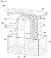
- the intelligent integrated assembly and transfer apparatus can include a fluid chamber 300, a roller unit 200 and assembly inspection unit 500.
- the fluid chamber 300 can accommodate semiconductor light emitting devices 150.
- Semiconductor light emitting devices 150 can be assembled on an assembly substrate 210.
- the assembly substrate 210 can be mounted on the roller unit 200.
- the roller unit 200 can rotate the assembly substrate 210.
- the assembly inspection unit 500 can inspect the semiconductor light emitting devices 150 assembled on the assembly substrate 210.
- the roller unit 200 can include a roller rotated part 220 where the assembly substrate 210 is mounted and rotated, a roller driving part 230 for rotating the roller rotated part 220, and a magnet head unit 400 for applying magnetic force to the semiconductor light emitting devices 150 to be assembled on the assembly substrate 210.
- the assembly inspection unit 500 can be controlled by inspecting an assembly status of each line in a width direction of the assembly substrate 210 so that a transfer process does not proceed to a panel substrate 910 in the case of unassembled or defective assembly.
- each line can be inspected in the width direction of the assembly substrate 210 and when there is an error position E of unassembled or defective assembly, a predetermined panel chuck separates the panel substrate 910 from the assembly substrate 210 such that the semiconductor light emitting device 150 in an error position is not transferred to the panel substrate 910.
- the panel chuck can be arranged on side, top, or bottom of the panel substrate 910 for separating the panel substrate 910 from the assembly substrate 210.
- the magnet head unit 400 can apply the magnetic force evenly to the semiconductor light emitting devices 150 by rotating or moving horizontally.
- the panel chuck can have a function of rotating the panel substrate 912 while the panel substrate 912 is in an inclined state.
- the intelligent integrated assembly and transfer apparatus further can have a panel driving unit 920B for driving to move the panel substrate 910.
- the panel driving unit 920B includes a second-first panel driving unit 920b 1 and a second-second panel driving unit 920b2, and the second-first panel driver (920b 1) is disposed at a different height from the second-second panel driving unit 920b2.
- the roller unit 900 can include a triangular shape or a round shape. And an area of the first-first roller part where the semiconductor light emitting devices 150 are assembled on the assembly substrate 210 is greater than the area of the first-second roller part where the semiconductor light emitting devices 150 are transferred to the panel substrate 910.
- the intelligent integrated assembly and transfer apparatus can further have a second magnet head unit 420 disposed under the fluid chamber 300.
- the intelligent integrated assembly and transfer apparatus of the semiconductor light emitting device there is a technical effect of simultaneously improving the transfer speed and the transfer yield in transferring the semiconductor light emitting devices to the display panel.
- the semiconductor light emitting device 150 can be assembled to the assembly substrate 210, and the assembled semiconductor light emitting devices 150 can be transferred in-line to the panel substrate 910 immediately so that the transfer speed can be significantly improved.
- the semiconductor light emitting devices 150 assembled on the assembly substrate 210 can be inspected in real time and then selectively transferred to the panel substrate 910 only when good, thereby significantly increasing the transfer yield.
- a portion where the assembly substrate 210 on the roller unit 200 and the flat panel substrate 910 meet may line transfer in the width direction of the roller unit 200.
- roller unit when configured in a multi-layer, there is an effect capable of implementing high-speed transfer.
- the display device described herein includes a mobile phone, a smart phone, a laptop computer, a terminal for digital broadcasting, a personal digital assistants (PDA), a portable multimedia player (PMP), navigation, a slate PC, Tablet PCs, Ultra-Books, digital TVs, desktop computers, and the like can be included.
- PDA personal digital assistants
- PMP portable multimedia player
- navigation a slate PC, Tablet PCs, Ultra-Books, digital TVs, desktop computers, and the like
- slate PC Portable multimedia player
- Tablet PCs Portable TVs
- desktop computers and the like
- the configuration according to the embodiment described in the present specification may be applied to a device capable of display, even in a new product form developed later.
- the semiconductor light emitting device applied in the embodiment and the display device using the same will be described (hereinafter, the 'first embodiment' is referred to as an 'embodiment').
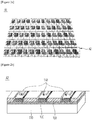
- FIG. 1 is an exemplary view in which the display device 100 according to an embodiment is disposed in a living room together with a washing machine 10, a robot cleaner 20, an air cleaner 30, and the like.
- the display device 100 of the embodiment can display the status of various electronic products such as the air cleaner 30, the robot cleaner 20, and the washing machine 10, and communicate with each electronic product based on IOT, and each electronic product may be controlled based on the setting data of the user.
- the display device 100 may include a flexible display manufactured on a thin flexible substrate.
- the flexible display may be bent or rolled like paper, while maintaining the characteristics of a flat panel display.
- visual information may be implemented by independently controlling light emission of unit pixels arranged in a matrix form.
- the unit pixel refers to a minimum unit for implementing one color.
- the unit pixel of the flexible display may be implemented by a semiconductor light emitting device.
- the semiconductor light emitting device may be a Micro-LED.
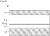
- FIG. 2A is an enlarged view of the area A1 in FIG. 1
- FIG. 2B is an enlarged view of the area A2 in FIG. 2A
- FIG. 2C is a cross-sectional view of the semiconductor light emitting device 150 in FIG. 2B .
- the display device 100 of the embodiment may drive a semiconductor light emitting device in an active matrix (AM) or passive matrix (PM) method.
- AM active matrix
- PM passive matrix
- the display device 100 of the embodiment may include a panel substrate 910, a first panel electrode 120, a second panel electrode (not shown), an insulating layer 130, and a plurality of semiconductor light emitting devices 150.
- Each of the semiconductor light emitting devices 150 may include red, green, and blue semiconductor light emitting devices to form a sub-pixel, but it is not limited thereto. And red color or green color can also be implemented with a red phosphor or a green phosphor respectively.
- the panel substrate 910 may be formed of glass or polyimide.
- the panel substrate 910 may include a flexible material such as PEN (Polyethylene Naphthalate), PET (Polyethylene Terephthalate).
- the panel substrate 910 may be a transparent material, but it is not limited thereto.
- the insulating layer 130 may include insulating and flexible materials such as polyimide, PEN, PET, and the like, and may be formed integrally with the panel substrate 910 to form a single substrate.
- the insulating layer 130 may be a conductive adhesive layer having adhesiveness and conductivity, and the conductive adhesive layer may have ductility to enable a flexible function of the display device.
- the insulating layer 130 may be an anisotropy conductive film (ACF) or a conductive adhesive layer such as an anisotropic conductive medium or a solution containing conductive particles.
- the conductive adhesive layer may be a layer that is electrically conductive in the vertical direction with respect to the thickness, but has electrical insulation in the horizontal direction with respect to the thickness.
- FIG. 2C is a cross-sectional view of a vertical type semiconductor light emitting device as an example of the semiconductor light emitting device 150 applied to the display device 100 of the embodiment.
- the semiconductor light emitting device that may be applied in the embodiment is not limited to a vertical type semiconductor light emitting device, and may include a lateral type semiconductor light emitting device or a flip type light emitting device.
- the semiconductor light emitting device applied in the embodiment is a pn junction diode in which electrical energy is converted into light energy, and may be made of a compound semiconductor containing elements of group III and group V on the periodic table.
- the band gap can be controlled by adjusting the composition ratio of the compound semiconductor such that various colors such as red, green and blue are possible.
- the semiconductor light emitting device 150 of the embodiment may include a light emitting structure 151, a first electrode 152a and a second electrode 152b.
- the light emitting structure 151 may include a first conductivity type semiconductor layer 151a, an active layer 151b, and a second conductivity type semiconductor layer 151c.
- a pad electrode (not shown) may be further disposed on the first electrode 152a or the second electrode 152b, but it is not limited thereto.
- At least one of the first electrode 152a or the second electrode 152b may include a magnetic material layer (not shown).
- the first conductivity type may be n-type, and the second conductivity type may be p-type, but it is not limited thereto.
- the magnetic material layer may include at least one of Ni, SmCo(samarium-cobalt), Gd-based, La-based, and Mn-based materials.
- the magnetic material layer may be disposed in a mesh form or in a dot form to have excellent light transmittance.
- One of the technical problems of the embodiment is to provide an intelligent integrated assembly and transfer apparatus capable of simultaneously improving the transfer speed and the transfer yield in transferring semiconductor light emitting devices to a display panel.
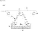
- FIG. 3 is a conceptual diagram of an intelligent integrated assembly and transfer apparatus 1000 according to an embodiment.
- FIG. 4 is an enlarged view of the region B1 of the assembly substrate 210 in the intelligent integrated assembly and transfer apparatus 1000 shown in FIG. 3 .
- FIGS. 5A and 5B are perspective views of the magnet head unit 400 in the intelligent integrated assembly and transfer apparatus 1000 shown in FIG. 3 .
- FIG. 6 is a diagram illustrating an operation of the intelligent integrated assembly and transfer apparatus 1000 according to the embodiment.
- the intelligent integrated assembly and transfer apparatus 1000 may include a hydrophilic treatment unit 600, a cleaning unit 700, a drying unit 800, and the like.
- the intelligent integrated assembly and transfer apparatus 1000 may include a panel chuck (not shown) for moving the panel substrate 910 horizontally and a panel driving unit 920 for horizontally moving the display panel substrate 910.
- the semiconductor light emitting device 150 can be assembled to the assembly substrate 210, and the assembled semiconductor light emitting devices 150 can be transferred in-line to the panel substrate 910 immediately so that the transfer speed can be significantly improved.
- the semiconductor light emitting devices 150 assembled on the assembly substrate 210 can be inspected in real time and then selectively transferred to the panel substrate 910 only when good, thereby significantly increasing the transfer yield. Accordingly, according to the embodiment, there is a special technical solving the problem of technical contradiction between the transfer speed and the transfer yield.
- the intelligent integrated assembly and transfer apparatus 1000 may include the fluid chamber 300 accommodating a plurality of semiconductor light emitting devices 150, the hydrophilic treatment unit 600, and the like.
- the fluid chamber 300 may be a water tank, and may be open or closed shape.
- the fluid chamber 300 may be filled with assembly solution such as deionized water, but it is not limited thereto.
- the hydrophilic treatment unit 600 may perform hydrophilic treatment for wetting before the assembly substrate 210 is inserted into the fluid.
- the embodiment may include an assembly substrate 210 mounted on the roller unit 200.
- the assembly substrate 210 may be referred to as a carrier substrate or a first transfer substrate.
- the assembly substrate 210 may be a flexible substrate that can be mounted on the roller rotated part 220.
- the assembly substrate 210 may be a flexible material that can be rolled, and may be a polymer such as polyimide or a thin metal substrate, but it is not limited thereto.
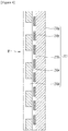
- FIG. 4 is an enlarged view of an area B1 of the assembly substrate 210 in the intelligent integrated assembly and transfer apparatus 1000 shown in FIG. 3 .
- the assembly substrate 210 may include a base portion 210a, a dielectric layer 210b, and a plurality of assembly electrodes 210c to form an electric field.
- the base portion 210a can be made of an insulating material, and the plurality of assembly electrodes 210c may be bi-planar electrodes of a thin film or a thick film patterned on one surface of the base portion 210a.
- the assembly electrode 210c may be formed of a stack of Ti/Cu/Ti, Ag paste, and ITO.
- the dielectric layer 210b may be made of inorganic materials such as SiO 2 , SiNx, SiON, Al 2 O 3 , TiO 2 , and HfO 2 .
- the dielectric layer 210b may be formed of a single layer or a multi-layer as an organic insulator.
- the assembly substrate 210 may include a plurality of cells 210d partitioned by the partition wall 210e.
- the cells 210d can be sequentially arranged along one direction, and may be formed of a polymer material.
- the partition wall 210e forming the cells 210d may be shared with neighboring cells 210d.
- the partition wall 210e may protrude upward from the base portion 210a, and the cells 210d may be sequentially arranged along one direction by the partition wall 210e.
- the cells 210d can be sequentially arranged in the column and row directions, respectively, and may have a matrix structure.
- the interior of the cells 210d may be an assembly groove for accommodating the semiconductor light emitting device 150, and the assembly groove may be a space partitioned by the partition wall 210e.
- the shape of the assembly groove may be the same or similar to the outer shape of the semiconductor light emitting device 150.
- the assembly groove may have a quadrangular shape.
- the assembly groove may be circular.
- one semiconductor light emitting device 150 may be accommodated in each cell.
- the plurality of assembly electrodes 210c includes a plurality of electrode lines disposed at the bottom of each cell 210d, and the plurality of electrode lines may be extended to neighboring cells.
- the plurality of assembly electrodes 210c may be disposed under the cells 210d, and different polarities may be applied to generate electric fields in the cells 210d.
- the dielectric layer 210b may cover the plurality of assembly electrodes 210c, and the dielectric layer 210b may form the bottom of the cells 210d.
- a power of a different polarity is applied to the pair of assembly electrodes 210c at the lower side of each cell 210d by a power supply unit (not shown), an electric field is formed, and the electric field generates the electric field into the cells 210d.
- the semiconductor light emitting device 150 may be accommodated and assembled.
- the intelligent integrated assembly and transfer apparatus 1000 may include a roller unit 200 that rotates the assembly substrate 210.
- the roller unit 200 may include a roller rotated part 220, a roller driving part 230, and a magnet head unit 400.
- the roller unit 200 includes a roller rotated part 220 on which an assembly substrate 210 is mounted and rotated, a roller driving part 230 driving the roller rotated part 220 to rotate, and may include a magnetic magnet head unit 400 applying a magnetic force to the semiconductor light emitting device 150 to be assembled to the assembly substrate 210.
- the roller unit 200 can make the semiconductor light emitting device 150 be transferred to the panel substrate 910 when the assembly substrate 210 and the panel substrate 910 meet in one line or a plurality of lines.
- the roller driving part 230 may rotate the roller rotated part 220 on which the assembly substrate 210 is mounted, and the roller driving part 230 may include a single or multiple motor, but it is not limited thereto.
- the roller rotated part 220 may be formed of a flexible material so that the mounted assembly substrate 210 can be rotated efficiently.
- the roller rotated part 220 may be in the form of a belt, but it is not limited thereto.
- the roller rotated part 220 may have a thickness of 5 mm or less so that the magnetic force of the magnet head unit 400 can be easily transmitted to the semiconductor light emitting device 150 while the assembly substrate 210 is mounted, but it is not limited thereto.
- the roller unit 200 may include a magnetic head part 400 that applies a magnetic force so that the semiconductor light emitting device 150 can be assembled to the assembly substrate 210.
- FIG. 5A is a perspective view of the magnet head unit 400 in the intelligent integrated assembly and transfer apparatus 1000 shown in FIG. 3
- FIG. 5B is a 180 degrees inverted perspective view of the magnet head unit 400 shown in FIG. 5A .
- the magnet head unit 400 may be located inside the roller unit 200 to function to induce the semiconductor light emitting device 150 in the fluid chamber 300 toward the assembly electrode 210c of the assembly substrate 210.
- the magnet head unit 400 may be one or a plurality.
- the magnet head unit 400 of the embodiment may include a plurality of magnets 410.
- the magnet 410 can be spaced apart from the fluid chamber 300 to apply a magnetic force to the semiconductor light emitting device 150, and the position may be controlled by a position controller (not shown) connected to the magnet 410.
- the magnet 410 may be a permanent magnet or an electromagnet.
- the embodiment may include a magnet handler (not shown) that can automatically or manually move the magnet head unit 400, or a magnet (not shown) that can rotate the magnet head unit 400 to provide a magnet.
- the magnet head unit 400 may be rotated (Z) clockwise or counterclockwise, and the magnet head unit 400 may be horizontally driven (XY) in a direction perpendicular to the rotation direction of the assembly substrate 210.
- the magnet head unit 400 may rotate to evenly distribute the magnetic force applied to the semiconductor light emitting device 150 to improve assembly speed.
- the magnet head unit 400 can distribute the magnetic force more evenly as it rotates while moving a certain section in the direction perpendicular to the rotation direction of the assembly substrate 210 to improve the assembly speed of the semiconductor light emitting device 150 and at the same time so that the semiconductor light emitting device 150 can be evenly assembled to the assembly substrate 210.
- the intelligent integrated assembly and transfer apparatus 1000 may include a cleaning unit 700, a drying unit 800, and an assembly inspection unit 500.
- the cleaning unit 700 may eject the semiconductor light emitting device 150 attached outside the assembly area of the assembly substrate 210 by spraying a solution in an area other than the assembly area of the assembly substrate 210.
- the cleaning unit 700 can spray the solution to cover the whole the line to remove the semiconductor light emitting devices 150 at a time.
- the drying unit 800 may apply hot air or heat to the semiconductor light emitting device 150 to evaporate the assembly solution before being transferred.
- the assembly inspection unit 500 may check whether the semiconductor light emitting device 150 is assembled or correctly assembled to the assembly substrate 210.
- the assembly inspection unit 500 may perform line scan assembly inspection, and cover the entire line at a time.
- the assembly inspection unit 500 may include a CCD image sensor, transmit the inspection results to a control unit (not shown), and determine whether to transfer the semiconductor light emitting device 150 to the panel substrate 910 according to the inspection results.
- FIG. 6 is a diagram illustrating an operation of the intelligent integrated assembly and transfer apparatus 1000 according to the embodiment.
- the intelligent integrated assembly and transfer apparatus 1000 may include a panel driving unit 920 for horizontally moving the display panel substrate 910 and a panel chuck (not shown) for vertically moving the panel substrate 910.
- the panel driving unit 920 may be provided in a single or plural form, and is illustrated in FIG. 6 as two, but it is not limited thereto.
- the panel driving unit 920 may be driven through a motor, but it is not limited thereto.
- the panel chuck can be disposed on at least one of a side surface, an upper surface, or a bottom surface of the panel substrate 910 to separate the panel substrate 910 from the assembly substrate 210.
- the assembly state of each line can be inspected in the width direction of the assembly substrate 210 to transfer line position information.
- the system control unit (not shown) can control the semiconductor light emitting device 150 on unassembled or defective assembly line not to be transferred to the panel substrate 910.
- the assembly inspection unit 500 can inspect the assembly state of each line in the width direction of the assembly substrate 210, and when there is an error position E such as unassembled or defective assembly, the panel substrate 910 can be moved upward by the panel chuck. By separating the assembly substrate 210 and the panel substrate 910, there is a special technical effect controlling the semiconductor light emitting device 150 on the error position E line not being transferred to the panel substrate 910.
- the semiconductor light emitting device 150 when the semiconductor light emitting device 150 is not assembled or properly assembled in the line-by-line pixels on the assembly substrate 210, the semiconductor light emitting device 150 on the corresponding Error line cannot be transferred to the panel substrate 910. There is a special technical effect simultaneously increasing the transfer speed and the transfer yield.
- FIG. 7 is a conceptual tilting view of the panel substrate 910 in the embodiment.
- the panel chuck may have a fine rotation function of the panel substrate 910 so that the semiconductor light emitting device 150 can be better transferred from the assembly substrate 210 to the panel substrate 910.
- the panel driving unit 920 may include a first-first panel driving unit 920a1 and a first-second panel driving unit 920a2.
- the height of the first-first panel driving unit 920a1 and the first-second panel driving unit 920a2 may be the same, and accordingly, the panel substrate 910 can be moved while maintaining the horizontal position, thereby causing the semiconductor light emitting device 150 to move.
- the second panel driving unit 920B includes a second-first panel driving unit 920b 1 and a second-second panel driving unit 920b2.
- the second-first panel driving unit 920b 1 may be disposed at a different height from the second-second panel driving unit 920b2.
- the second-first panel driving unit 920b1 may be disposed lower than the second-second panel driving unit 920b2. Accordingly, a front end 912b1 of the second panel substrate 912 may be disposed lower than a rear end 912b2. As the second panel substrate 912 can be moved in an inclined state, transferring of the semiconductor light emitting device 150 can be more effectively performed. Accordingly, the semiconductor light emitting device 150 can be more effectively transferred from the assembly substrate 210 to the second panel substrate 912.
- a portion where the assembly substrate 210 on the roller unit 200 and the flat panel substrate 910 meet may line transfer in the width direction of the roller unit 200.
- the defective assembly substrate or defective semiconductor light emitting device can be avoided to be transferred, thereby minimizing the dependence on the quality of the semiconductor light emitting device.
- roller unit when configured in a multi-layer, there is an effect capable of implementing high-speed transfer.
- the semiconductor light emitting device 150 can be introduced into the fluid chamber 300, and the assembly substrate 210 can be mounted on the roller unit 200.
- a magnetic force can be applied to the semiconductor light emitting device 150 using the magnet head unit 400 so that the semiconductor light emitting device 150 can float in the vertical direction in the fluid chamber 300.
- the separation distance between the assembly surface of the assembly substrate 210 and the semiconductor light emitting device 150 may be controlled.
- the separation distance may be controlled using the weight, buoyancy, and magnetic force of the semiconductor light emitting device 150.
- a magnetic force can be applied to the semiconductor light emitting device 150 so that the semiconductor light emitting device 150 can move along one direction in the fluid chamber 300.
- the magnet of the magnet head unit 400 may be rotated clockwise or counterclockwise while moving in the direction perpendicular to the rotational direction of the assembly substrate 210.
- a step of applying an electric field to the semiconductor light emitting device 150 so as to be seated at the assembly position of the assembly substrate 210 is conducted.
- the semiconductor light emitting device 150 moves along the assembly substrate 210, the semiconductor light emitting device 150 can rest on an assembly position of the assembly substrate 210 by moving in a vertical or horizontal direction with the assembly substrate 210 by an electric field.
- an electric field may be generated by supplying power to the bi-planar electrode of the assembly substrate 210, and the assembly may be controlled to be assembled only at the assembly position. That is, by using the selectively generated electric field, the semiconductor light emitting device 150 can be self-assembled at the assembly position of the assembly substrate 210.
- the cleaning unit 700 may eject the semiconductor light emitting device 150 attached outside the assembly area of the assembly substrate 210 by spraying a solution outside the assembly area so that the entire line can be covered at one time.
- the drying unit 800 may apply hot air or heat to the assembled semiconductor light emitting device 150 to make the assembly solution to evaporate before be transferring.
- the assembly inspection unit 500 may inspect whether the semiconductor light emitting device 150 is assembled to the assembly substrate 210 or not.
- the assembly inspection unit 500 may perform line scan assembly inspection, and may cover the entire line at a time.
- the assembly inspection unit 500 may include a CCD image sensor, transmit inspection results to a control unit, and determine whether to transfer the semiconductor light emitting device 150 to the panel substrate 910 according to the inspection results.
- line position information in the case of unassembled or defective assembly can be inspected by inspecting the assembly state of each line in the width direction of the assembly substrate 210 so that the unassembled or defective assembly line does not proceed to be transferred to the panel substrate 910.
- the panel substrate 910 can be moved upward through the panel chuck when there is an error position E such as unassembled or defective assembly.
- an error position E such as unassembled or defective assembly.
- the semiconductor light emitting device 150 when the semiconductor light emitting device 150 is not assembled or properly assembled among the pixels for each line on the assembly substrate 210, the semiconductor light emitting device 150 on the corresponding Error line is not transferred to the panel substrate 910. There is a special technical effect simultaneously increasing the transfer speed and the transfer yield.
- a post process for implementing the display device may be performed on the semiconductor light emitting device 150 transferred to the panel substrate 910.
- FIGs. 8A to 8C are conceptual diagrams of the intelligent integrated assembly and transfer apparatus 1000 according to a second embodiment.
- the second embodiment may employ the technical features of the first embodiment, but will be described below mainly on the main features of the second embodiment.
- the intelligent integrated assembly and transfer apparatus according to the second embodiment is an embodiment for another form of the roller unit.
- the second-first roller unit 200a may have a circular shape, and the roller driving part 230 may be provided in one or a plurality.
- the curvature at the time of assembly and the curvature at the time of transfer may be differently controlled.
- the second-second roller unit 200b may have a triangular shape, and the roller driving part 230 may be provided in one or more.
- the contact area between the semiconductor light emitting device 150 and the assembly substrate 210 can be widened.
- the assembly speed can be increased, and in the transfer region where the semiconductor light emitting device 150 is transferred to the panel substrate 910, the transfer accuracy can be increased by making the panel substrate 910 and the assembly substrate 210 contact each line.
- the second-third roller unit 200c may include a flat roller part 200c1 and a round roller part 200c2, and the roller drive part 230 may be provided in one or a plurality.
- the assembly speed can be increased by widening the contact area between the semiconductor light emitting device 150 and the assembly substrate 210 through the round roller part 200c2.
- the transfer accuracy can be increased by making the panel substrate 910 and the assembly substrate 210 contact each line.
- the curvature at the time of assembly and the curvature at the time of transfer may be differently controlled.
- the assembly speed may be increased by widening the contact area with the assembly substrate 210, and the transfer accuracy can be increased by making assembly substrate 210 contact with the panel substrate 910 by line in the transfer area.
- FIG. 9 is a conceptual diagram of an intelligent integrated assembly and transfer apparatus 1003 according to a third embodiment.
- the third embodiment can adopt the technical features of the first and second embodiments.
- a second magnet head unit 420 can be disposed under the fluid chamber 300.
- the second magnet head unit 420 may include a permanent magnet or an electromagnet.
- the assembly position of the semiconductor light emitting device 150 can be rotated the upper side or lower side of the semiconductor light emitting device 150 by the second magnet head 420 disposed under the fluid chamber 300.
- the second magnet head 420 disposed under the fluid chamber 300.
- the intelligent integrated assembly and transfer apparatus of the semiconductor light emitting device there is a technical effect of simultaneously improving the transfer speed and the transfer yield in transferring the semiconductor light emitting devices to the display panel.
- the semiconductor light emitting device 150 can be assembled to the assembly substrate 210, and the assembled semiconductor light emitting devices 150 can be transferred in-line to the panel substrate 910 immediately so that the transfer speed can be significantly improved.
- the semiconductor light emitting devices 150 assembled on the assembly substrate 210 can be inspected in real time and then selectively transferred to the panel substrate 910 only when good, thereby significantly increasing the transfer yield.
- a portion where the assembly substrate 210 on the roller unit 200 and the flat panel substrate 910 meet may line transfer in the width direction of the roller unit 200.
- roller unit when configured in a multi-layer, there is an effect capable of implementing high-speed transfer.
Landscapes
- Led Device Packages (AREA)
- Electroluminescent Light Sources (AREA)
Applications Claiming Priority (1)
| Application Number | Priority Date | Filing Date | Title |
|---|---|---|---|
| KR1020200057811A KR102796435B1 (ko) | 2020-05-14 | 2020-05-14 | 반도체 발광소자의 지능형 조립전사 통합장치 |
Publications (2)
| Publication Number | Publication Date |
|---|---|
| EP3910665A1 true EP3910665A1 (de) | 2021-11-17 |
| EP3910665B1 EP3910665B1 (de) | 2024-06-12 |
Family
ID=71943939
Family Applications (1)
| Application Number | Title | Priority Date | Filing Date |
|---|---|---|---|
| EP20189076.1A Active EP3910665B1 (de) | 2020-05-14 | 2020-08-03 | Intelligente integrierte anordnung und übertragungsvorrichtung für lichtemittierendes halbleiterbauelement |
Country Status (4)
| Country | Link |
|---|---|
| US (1) | US11996393B2 (de) |
| EP (1) | EP3910665B1 (de) |
| KR (1) | KR102796435B1 (de) |
| CN (1) | CN113675126B (de) |
Cited By (1)
| Publication number | Priority date | Publication date | Assignee | Title |
|---|---|---|---|---|
| US20210358893A1 (en) * | 2020-05-14 | 2021-11-18 | Lg Electronics Inc. | Intelligent integrated assembly and transfer apparatus for semiconductor light emitting device |
Families Citing this family (5)
| Publication number | Priority date | Publication date | Assignee | Title |
|---|---|---|---|---|
| KR102834044B1 (ko) | 2021-02-03 | 2025-07-16 | 엘지전자 주식회사 | 반도체 발광소자의 전사용 롤러부의 전극구조 및 이를포함하는 지능형 조립전사 통합장치 |
| CN115312443A (zh) * | 2021-05-06 | 2022-11-08 | 台湾爱司帝科技股份有限公司 | 电子组件转移装置、电子组件转移方法、以及发光二极管面板的制造方法 |
| KR102752104B1 (ko) * | 2022-01-06 | 2025-01-10 | 엘지전자 주식회사 | 3차원 구동이 가능한 반도체 발광소자 전사용 마그넷 구동장치 및 이를 포함하는 지능형 조립전사 통합장치 |
| KR102857453B1 (ko) | 2022-07-04 | 2025-09-08 | 삼성전자주식회사 | 칩 습식 전사 장치 |
| US20250176343A1 (en) * | 2022-12-28 | 2025-05-29 | Seoul National University R&Db Foundation | Micro led array electronic device and its transfer method |
Citations (6)
| Publication number | Priority date | Publication date | Assignee | Title |
|---|---|---|---|---|
| EP1801046A1 (de) * | 2004-09-22 | 2007-06-27 | Hallys Corporation | Übertragungsvorrichtung |
| US20090218260A1 (en) * | 2008-03-03 | 2009-09-03 | Palo Alto Research Center, Incorporated | Micro-assembler |
| WO2013158949A1 (en) * | 2012-04-20 | 2013-10-24 | Rensselaer Polytechnic Institute | Light emitting diodes and a method of packaging the same |
| EP2688093A1 (de) * | 2012-07-19 | 2014-01-22 | Technische Universität Ilmenau | Verfahren und Vorrichtung zur Selbstmontage von Komponenten auf einem Substrat |
| US9825202B2 (en) | 2014-10-31 | 2017-11-21 | eLux, Inc. | Display with surface mount emissive elements |
| KR20200014866A (ko) * | 2020-01-22 | 2020-02-11 | 엘지전자 주식회사 | 자가 조립용 칩 트레이 및 반도체 발광소자의 공급 방법 |
Family Cites Families (5)
| Publication number | Priority date | Publication date | Assignee | Title |
|---|---|---|---|---|
| WO2017078368A1 (ko) * | 2015-11-05 | 2017-05-11 | 서울바이오시스주식회사 | 자외선 발광 소자 및 그것을 제조하는 방법 |
| CN107833525B (zh) * | 2016-09-15 | 2020-10-27 | 伊乐视有限公司 | 发光显示器的流体组装的系统和方法 |
| DE102016011747B4 (de) * | 2016-09-29 | 2018-06-07 | Mühlbauer Gmbh & Co. Kg | Vorrichtung und Verfahren zum berührungslosen Übertragen von zumindest teilweise ferromagnetischen elektronischen Bauteilen von einem Träger zu einem Subtrat |
| KR102733058B1 (ko) * | 2019-05-22 | 2024-11-21 | 엘지전자 주식회사 | 반도체 발광소자의 자가조립 장치 및 방법 |
| KR102796435B1 (ko) * | 2020-05-14 | 2025-04-16 | 엘지전자 주식회사 | 반도체 발광소자의 지능형 조립전사 통합장치 |
-
2020
- 2020-05-14 KR KR1020200057811A patent/KR102796435B1/ko active Active
- 2020-08-03 EP EP20189076.1A patent/EP3910665B1/de active Active
- 2020-09-04 US US17/013,201 patent/US11996393B2/en active Active
- 2020-10-12 CN CN202011085096.8A patent/CN113675126B/zh active Active
Patent Citations (6)
| Publication number | Priority date | Publication date | Assignee | Title |
|---|---|---|---|---|
| EP1801046A1 (de) * | 2004-09-22 | 2007-06-27 | Hallys Corporation | Übertragungsvorrichtung |
| US20090218260A1 (en) * | 2008-03-03 | 2009-09-03 | Palo Alto Research Center, Incorporated | Micro-assembler |
| WO2013158949A1 (en) * | 2012-04-20 | 2013-10-24 | Rensselaer Polytechnic Institute | Light emitting diodes and a method of packaging the same |
| EP2688093A1 (de) * | 2012-07-19 | 2014-01-22 | Technische Universität Ilmenau | Verfahren und Vorrichtung zur Selbstmontage von Komponenten auf einem Substrat |
| US9825202B2 (en) | 2014-10-31 | 2017-11-21 | eLux, Inc. | Display with surface mount emissive elements |
| KR20200014866A (ko) * | 2020-01-22 | 2020-02-11 | 엘지전자 주식회사 | 자가 조립용 칩 트레이 및 반도체 발광소자의 공급 방법 |
Cited By (2)
| Publication number | Priority date | Publication date | Assignee | Title |
|---|---|---|---|---|
| US20210358893A1 (en) * | 2020-05-14 | 2021-11-18 | Lg Electronics Inc. | Intelligent integrated assembly and transfer apparatus for semiconductor light emitting device |
| US11996393B2 (en) * | 2020-05-14 | 2024-05-28 | Lg Electronics Inc. | Intelligent integrated assembly and transfer apparatus for semiconductor light emitting device |
Also Published As
| Publication number | Publication date |
|---|---|
| KR20210140956A (ko) | 2021-11-23 |
| EP3910665B1 (de) | 2024-06-12 |
| KR102796435B1 (ko) | 2025-04-16 |
| CN113675126B (zh) | 2023-08-25 |
| US11996393B2 (en) | 2024-05-28 |
| CN113675126A (zh) | 2021-11-19 |
| US20210358893A1 (en) | 2021-11-18 |
Similar Documents
| Publication | Publication Date | Title |
|---|---|---|
| US11996393B2 (en) | Intelligent integrated assembly and transfer apparatus for semiconductor light emitting device | |
| EP4174944B1 (de) | Anzeigevorrichtung mit einer lichtemittierenden halbleitervorrichtung | |
| US20230130868A1 (en) | Display device including semiconductor light emitting device | |
| KR102783683B1 (ko) | 반도체 발광소자를 포함하는 디스플레이 장치 | |
| KR20240134331A (ko) | 반도체 발광소자의 디스플레이 장치 | |
| KR20240122809A (ko) | 반도체 발광소자 디스플레이 장치의 조립기판 구조 및 이를 포함하는 디스플레이 장치 | |
| US12538736B2 (en) | Electrode structure of roller unit for transferring semiconductor light-emitting element and intelligent integrated assembling and transferring device comprising same | |
| KR102931255B1 (ko) | 반도체 발광소자의 전사를 위한 조립 기판, 반도체 발광소자가 전사된 패널 기판 및 이를 포함하는 디스플레이 장치 | |
| KR102752104B1 (ko) | 3차원 구동이 가능한 반도체 발광소자 전사용 마그넷 구동장치 및 이를 포함하는 지능형 조립전사 통합장치 | |
| KR102732210B1 (ko) | 디스플레이 화소용 반도체 발광소자의 균일 군집 공급장치 및 이를 이용한 자가 조립장치 | |
| KR102931254B1 (ko) | 반도체 발광소자를 포함하는 디스플레이 장치 | |
| KR102746626B1 (ko) | 디스플레이 화소용 반도체 발광소자의 마그넷 유닛 및 이를 이용한 자가 조립 장치 | |
| KR102917620B1 (ko) | 반도체 발광소자의 전사용 기판 및 이를 이용한 전사 방법 | |
| US12525593B2 (en) | Assembly substrate structure of semiconductor light emitting device display device and display device including the same | |
| KR102698079B1 (ko) | 화소용 반도체 발광소자의 전사를 위한 기판 구조 및 이를 포함하는 디스플레이 장치 | |
| EP4571837A1 (de) | Anzeigevorrichtung | |
| US20240038824A1 (en) | Assembly substrate structure of a display device including a semiconductor light emitting device and a display device including the same | |
| KR20250133918A (ko) | 화소용 반도체 발광소자의 마그넷 조립장치 및 이를 포함하는 디스플레이 화소용 반도체 발광소자의 자가 조립 장치 | |
| KR20250178375A (ko) | 반도체 발광소자를 포함하는 디스플레이 장치 | |
| KR20250061264A (ko) | 디스플레이 화소용 반도체 발광소자의 전사용 기판 및 이를 포함하는 디스플레이 장치 | |
| KR20250179126A (ko) | 반도체 발광소자를 포함하는 디스플레이 장치 및 이의 제조방법 | |
| KR20250115036A (ko) | 디스플레이 화소용 반도체 발광소자 패키지 및 이를 포함하는 조립용 기판 및 이의 조립방법 | |
| KR20250042009A (ko) | 반도체 발광소자 및 이를 포함하는 디스플레이 장치 | |
| CN121773729A (zh) | 发光元件、其制造方法及利用该发光元件的显示器装置 | |
| CN119999361A (zh) | 显示装置 |
Legal Events
| Date | Code | Title | Description |
|---|---|---|---|
| PUAI | Public reference made under article 153(3) epc to a published international application that has entered the european phase |
Free format text: ORIGINAL CODE: 0009012 |
|
| STAA | Information on the status of an ep patent application or granted ep patent |
Free format text: STATUS: REQUEST FOR EXAMINATION WAS MADE |
|
| 17P | Request for examination filed |
Effective date: 20200803 |
|
| AK | Designated contracting states |
Kind code of ref document: A1 Designated state(s): AL AT BE BG CH CY CZ DE DK EE ES FI FR GB GR HR HU IE IS IT LI LT LU LV MC MK MT NL NO PL PT RO RS SE SI SK SM TR |
|
| B565 | Issuance of search results under rule 164(2) epc |
Effective date: 20210208 |
|
| RBV | Designated contracting states (corrected) |
Designated state(s): AL AT BE BG CH CY CZ DE DK EE ES FI FR GB GR HR HU IE IS IT LI LT LU LV MC MK MT NL NO PL PT RO RS SE SI SK SM TR |
|
| GRAP | Despatch of communication of intention to grant a patent |
Free format text: ORIGINAL CODE: EPIDOSNIGR1 |
|
| STAA | Information on the status of an ep patent application or granted ep patent |
Free format text: STATUS: GRANT OF PATENT IS INTENDED |
|
| INTG | Intention to grant announced |
Effective date: 20240124 |
|
| GRAS | Grant fee paid |
Free format text: ORIGINAL CODE: EPIDOSNIGR3 |
|
| GRAA | (expected) grant |
Free format text: ORIGINAL CODE: 0009210 |
|
| STAA | Information on the status of an ep patent application or granted ep patent |
Free format text: STATUS: THE PATENT HAS BEEN GRANTED |
|
| AK | Designated contracting states |
Kind code of ref document: B1 Designated state(s): AL AT BE BG CH CY CZ DE DK EE ES FI FR GB GR HR HU IE IS IT LI LT LU LV MC MK MT NL NO PL PT RO RS SE SI SK SM TR |
|
| REG | Reference to a national code |
Ref country code: GB Ref legal event code: FG4D |
|
| REG | Reference to a national code |
Ref country code: CH Ref legal event code: EP |
|
| REG | Reference to a national code |
Ref country code: IE Ref legal event code: FG4D |
|
| REG | Reference to a national code |
Ref country code: DE Ref legal event code: R096 Ref document number: 602020032205 Country of ref document: DE |
|
| PG25 | Lapsed in a contracting state [announced via postgrant information from national office to epo] |
Ref country code: BG Free format text: LAPSE BECAUSE OF FAILURE TO SUBMIT A TRANSLATION OF THE DESCRIPTION OR TO PAY THE FEE WITHIN THE PRESCRIBED TIME-LIMIT Effective date: 20240612 |
|
| PG25 | Lapsed in a contracting state [announced via postgrant information from national office to epo] |
Ref country code: FI Free format text: LAPSE BECAUSE OF FAILURE TO SUBMIT A TRANSLATION OF THE DESCRIPTION OR TO PAY THE FEE WITHIN THE PRESCRIBED TIME-LIMIT Effective date: 20240612 Ref country code: HR Free format text: LAPSE BECAUSE OF FAILURE TO SUBMIT A TRANSLATION OF THE DESCRIPTION OR TO PAY THE FEE WITHIN THE PRESCRIBED TIME-LIMIT Effective date: 20240612 |
|
| REG | Reference to a national code |
Ref country code: LT Ref legal event code: MG9D |
|
| PG25 | Lapsed in a contracting state [announced via postgrant information from national office to epo] |
Ref country code: GR Free format text: LAPSE BECAUSE OF FAILURE TO SUBMIT A TRANSLATION OF THE DESCRIPTION OR TO PAY THE FEE WITHIN THE PRESCRIBED TIME-LIMIT Effective date: 20240913 |
|
| PG25 | Lapsed in a contracting state [announced via postgrant information from national office to epo] |
Ref country code: ES Free format text: LAPSE BECAUSE OF FAILURE TO SUBMIT A TRANSLATION OF THE DESCRIPTION OR TO PAY THE FEE WITHIN THE PRESCRIBED TIME-LIMIT Effective date: 20240612 |
|
| PG25 | Lapsed in a contracting state [announced via postgrant information from national office to epo] |
Ref country code: LV Free format text: LAPSE BECAUSE OF FAILURE TO SUBMIT A TRANSLATION OF THE DESCRIPTION OR TO PAY THE FEE WITHIN THE PRESCRIBED TIME-LIMIT Effective date: 20240612 |
|
| PG25 | Lapsed in a contracting state [announced via postgrant information from national office to epo] |
Ref country code: NO Free format text: LAPSE BECAUSE OF FAILURE TO SUBMIT A TRANSLATION OF THE DESCRIPTION OR TO PAY THE FEE WITHIN THE PRESCRIBED TIME-LIMIT Effective date: 20240912 Ref country code: LV Free format text: LAPSE BECAUSE OF FAILURE TO SUBMIT A TRANSLATION OF THE DESCRIPTION OR TO PAY THE FEE WITHIN THE PRESCRIBED TIME-LIMIT Effective date: 20240612 Ref country code: HR Free format text: LAPSE BECAUSE OF FAILURE TO SUBMIT A TRANSLATION OF THE DESCRIPTION OR TO PAY THE FEE WITHIN THE PRESCRIBED TIME-LIMIT Effective date: 20240612 Ref country code: GR Free format text: LAPSE BECAUSE OF FAILURE TO SUBMIT A TRANSLATION OF THE DESCRIPTION OR TO PAY THE FEE WITHIN THE PRESCRIBED TIME-LIMIT Effective date: 20240913 Ref country code: FI Free format text: LAPSE BECAUSE OF FAILURE TO SUBMIT A TRANSLATION OF THE DESCRIPTION OR TO PAY THE FEE WITHIN THE PRESCRIBED TIME-LIMIT Effective date: 20240612 Ref country code: ES Free format text: LAPSE BECAUSE OF FAILURE TO SUBMIT A TRANSLATION OF THE DESCRIPTION OR TO PAY THE FEE WITHIN THE PRESCRIBED TIME-LIMIT Effective date: 20240612 Ref country code: BG Free format text: LAPSE BECAUSE OF FAILURE TO SUBMIT A TRANSLATION OF THE DESCRIPTION OR TO PAY THE FEE WITHIN THE PRESCRIBED TIME-LIMIT Effective date: 20240612 Ref country code: RS Free format text: LAPSE BECAUSE OF FAILURE TO SUBMIT A TRANSLATION OF THE DESCRIPTION OR TO PAY THE FEE WITHIN THE PRESCRIBED TIME-LIMIT Effective date: 20240912 |
|
| PG25 | Lapsed in a contracting state [announced via postgrant information from national office to epo] |
Ref country code: NL Free format text: LAPSE BECAUSE OF FAILURE TO SUBMIT A TRANSLATION OF THE DESCRIPTION OR TO PAY THE FEE WITHIN THE PRESCRIBED TIME-LIMIT Effective date: 20240612 |
|
| REG | Reference to a national code |
Ref country code: AT Ref legal event code: MK05 Ref document number: 1694959 Country of ref document: AT Kind code of ref document: T Effective date: 20240612 |
|
| PG25 | Lapsed in a contracting state [announced via postgrant information from national office to epo] |
Ref country code: NL Free format text: LAPSE BECAUSE OF FAILURE TO SUBMIT A TRANSLATION OF THE DESCRIPTION OR TO PAY THE FEE WITHIN THE PRESCRIBED TIME-LIMIT Effective date: 20240612 |
|
| PG25 | Lapsed in a contracting state [announced via postgrant information from national office to epo] |
Ref country code: PT Free format text: LAPSE BECAUSE OF FAILURE TO SUBMIT A TRANSLATION OF THE DESCRIPTION OR TO PAY THE FEE WITHIN THE PRESCRIBED TIME-LIMIT Effective date: 20241014 |
|
| PG25 | Lapsed in a contracting state [announced via postgrant information from national office to epo] |
Ref country code: PT Free format text: LAPSE BECAUSE OF FAILURE TO SUBMIT A TRANSLATION OF THE DESCRIPTION OR TO PAY THE FEE WITHIN THE PRESCRIBED TIME-LIMIT Effective date: 20241014 |
|
| PG25 | Lapsed in a contracting state [announced via postgrant information from national office to epo] |
Ref country code: PL Free format text: LAPSE BECAUSE OF FAILURE TO SUBMIT A TRANSLATION OF THE DESCRIPTION OR TO PAY THE FEE WITHIN THE PRESCRIBED TIME-LIMIT Effective date: 20240612 |
|
| PG25 | Lapsed in a contracting state [announced via postgrant information from national office to epo] |
Ref country code: EE Free format text: LAPSE BECAUSE OF FAILURE TO SUBMIT A TRANSLATION OF THE DESCRIPTION OR TO PAY THE FEE WITHIN THE PRESCRIBED TIME-LIMIT Effective date: 20240612 |
|
| PG25 | Lapsed in a contracting state [announced via postgrant information from national office to epo] |
Ref country code: AT Free format text: LAPSE BECAUSE OF FAILURE TO SUBMIT A TRANSLATION OF THE DESCRIPTION OR TO PAY THE FEE WITHIN THE PRESCRIBED TIME-LIMIT Effective date: 20240612 Ref country code: IS Free format text: LAPSE BECAUSE OF FAILURE TO SUBMIT A TRANSLATION OF THE DESCRIPTION OR TO PAY THE FEE WITHIN THE PRESCRIBED TIME-LIMIT Effective date: 20241012 |
|
| PG25 | Lapsed in a contracting state [announced via postgrant information from national office to epo] |
Ref country code: CZ Free format text: LAPSE BECAUSE OF FAILURE TO SUBMIT A TRANSLATION OF THE DESCRIPTION OR TO PAY THE FEE WITHIN THE PRESCRIBED TIME-LIMIT Effective date: 20240612 |
|
| PG25 | Lapsed in a contracting state [announced via postgrant information from national office to epo] |
Ref country code: SK Free format text: LAPSE BECAUSE OF FAILURE TO SUBMIT A TRANSLATION OF THE DESCRIPTION OR TO PAY THE FEE WITHIN THE PRESCRIBED TIME-LIMIT Effective date: 20240612 Ref country code: RO Free format text: LAPSE BECAUSE OF FAILURE TO SUBMIT A TRANSLATION OF THE DESCRIPTION OR TO PAY THE FEE WITHIN THE PRESCRIBED TIME-LIMIT Effective date: 20240612 |
|
| PG25 | Lapsed in a contracting state [announced via postgrant information from national office to epo] |
Ref country code: SM Free format text: LAPSE BECAUSE OF FAILURE TO SUBMIT A TRANSLATION OF THE DESCRIPTION OR TO PAY THE FEE WITHIN THE PRESCRIBED TIME-LIMIT Effective date: 20240612 |
|
| PG25 | Lapsed in a contracting state [announced via postgrant information from national office to epo] |
Ref country code: SM Free format text: LAPSE BECAUSE OF FAILURE TO SUBMIT A TRANSLATION OF THE DESCRIPTION OR TO PAY THE FEE WITHIN THE PRESCRIBED TIME-LIMIT Effective date: 20240612 Ref country code: SK Free format text: LAPSE BECAUSE OF FAILURE TO SUBMIT A TRANSLATION OF THE DESCRIPTION OR TO PAY THE FEE WITHIN THE PRESCRIBED TIME-LIMIT Effective date: 20240612 Ref country code: RO Free format text: LAPSE BECAUSE OF FAILURE TO SUBMIT A TRANSLATION OF THE DESCRIPTION OR TO PAY THE FEE WITHIN THE PRESCRIBED TIME-LIMIT Effective date: 20240612 Ref country code: PL Free format text: LAPSE BECAUSE OF FAILURE TO SUBMIT A TRANSLATION OF THE DESCRIPTION OR TO PAY THE FEE WITHIN THE PRESCRIBED TIME-LIMIT Effective date: 20240612 Ref country code: IS Free format text: LAPSE BECAUSE OF FAILURE TO SUBMIT A TRANSLATION OF THE DESCRIPTION OR TO PAY THE FEE WITHIN THE PRESCRIBED TIME-LIMIT Effective date: 20241012 Ref country code: EE Free format text: LAPSE BECAUSE OF FAILURE TO SUBMIT A TRANSLATION OF THE DESCRIPTION OR TO PAY THE FEE WITHIN THE PRESCRIBED TIME-LIMIT Effective date: 20240612 Ref country code: CZ Free format text: LAPSE BECAUSE OF FAILURE TO SUBMIT A TRANSLATION OF THE DESCRIPTION OR TO PAY THE FEE WITHIN THE PRESCRIBED TIME-LIMIT Effective date: 20240612 Ref country code: AT Free format text: LAPSE BECAUSE OF FAILURE TO SUBMIT A TRANSLATION OF THE DESCRIPTION OR TO PAY THE FEE WITHIN THE PRESCRIBED TIME-LIMIT Effective date: 20240612 |
|
| PG25 | Lapsed in a contracting state [announced via postgrant information from national office to epo] |
Ref country code: IT Free format text: LAPSE BECAUSE OF FAILURE TO SUBMIT A TRANSLATION OF THE DESCRIPTION OR TO PAY THE FEE WITHIN THE PRESCRIBED TIME-LIMIT Effective date: 20240612 |
|
| REG | Reference to a national code |
Ref country code: DE Ref legal event code: R097 Ref document number: 602020032205 Country of ref document: DE |
|
| REG | Reference to a national code |
Ref country code: CH Ref legal event code: PL |
|
| PG25 | Lapsed in a contracting state [announced via postgrant information from national office to epo] |
Ref country code: DK Free format text: LAPSE BECAUSE OF FAILURE TO SUBMIT A TRANSLATION OF THE DESCRIPTION OR TO PAY THE FEE WITHIN THE PRESCRIBED TIME-LIMIT Effective date: 20240612 |
|
| PG25 | Lapsed in a contracting state [announced via postgrant information from national office to epo] |
Ref country code: LU Free format text: LAPSE BECAUSE OF NON-PAYMENT OF DUE FEES Effective date: 20240803 |
|
| PLBE | No opposition filed within time limit |
Free format text: ORIGINAL CODE: 0009261 |
|
| STAA | Information on the status of an ep patent application or granted ep patent |
Free format text: STATUS: NO OPPOSITION FILED WITHIN TIME LIMIT |
|
| PG25 | Lapsed in a contracting state [announced via postgrant information from national office to epo] |
Ref country code: MC Free format text: LAPSE BECAUSE OF FAILURE TO SUBMIT A TRANSLATION OF THE DESCRIPTION OR TO PAY THE FEE WITHIN THE PRESCRIBED TIME-LIMIT Effective date: 20240612 Ref country code: CH Free format text: LAPSE BECAUSE OF NON-PAYMENT OF DUE FEES Effective date: 20240831 |
|
| 26N | No opposition filed |
Effective date: 20250313 |
|
| GBPC | Gb: european patent ceased through non-payment of renewal fee |
Effective date: 20240912 |
|
| REG | Reference to a national code |
Ref country code: BE Ref legal event code: MM Effective date: 20240831 |
|
| PG25 | Lapsed in a contracting state [announced via postgrant information from national office to epo] |
Ref country code: GB Free format text: LAPSE BECAUSE OF NON-PAYMENT OF DUE FEES Effective date: 20240912 |
|
| PG25 | Lapsed in a contracting state [announced via postgrant information from national office to epo] |
Ref country code: BE Free format text: LAPSE BECAUSE OF NON-PAYMENT OF DUE FEES Effective date: 20240831 |
|
| PG25 | Lapsed in a contracting state [announced via postgrant information from national office to epo] |
Ref country code: FR Free format text: LAPSE BECAUSE OF NON-PAYMENT OF DUE FEES Effective date: 20240812 |
|
| PG25 | Lapsed in a contracting state [announced via postgrant information from national office to epo] |
Ref country code: IE Free format text: LAPSE BECAUSE OF NON-PAYMENT OF DUE FEES Effective date: 20240803 |
|
| PG25 | Lapsed in a contracting state [announced via postgrant information from national office to epo] |
Ref country code: SE Free format text: LAPSE BECAUSE OF FAILURE TO SUBMIT A TRANSLATION OF THE DESCRIPTION OR TO PAY THE FEE WITHIN THE PRESCRIBED TIME-LIMIT Effective date: 20240612 |
|
| PGFP | Annual fee paid to national office [announced via postgrant information from national office to epo] |
Ref country code: DE Payment date: 20250707 Year of fee payment: 6 |
|
| REG | Reference to a national code |
Ref country code: DE Ref legal event code: R079 Ref document number: 602020032205 Country of ref document: DE Free format text: PREVIOUS MAIN CLASS: H01L0021670000 Ipc: H10P0072000000 |
|
| PG25 | Lapsed in a contracting state [announced via postgrant information from national office to epo] |
Ref country code: CY Free format text: LAPSE BECAUSE OF FAILURE TO SUBMIT A TRANSLATION OF THE DESCRIPTION OR TO PAY THE FEE WITHIN THE PRESCRIBED TIME-LIMIT; INVALID AB INITIO Effective date: 20200803 |
|
| PG25 | Lapsed in a contracting state [announced via postgrant information from national office to epo] |
Ref country code: HU Free format text: LAPSE BECAUSE OF FAILURE TO SUBMIT A TRANSLATION OF THE DESCRIPTION OR TO PAY THE FEE WITHIN THE PRESCRIBED TIME-LIMIT; INVALID AB INITIO Effective date: 20200803 |