EP2690771A2 - Dispositif d'alimentation électrique, dispositif d'éclairage, appareil d'éclairage l'utilisant et véhicule - Google Patents
Dispositif d'alimentation électrique, dispositif d'éclairage, appareil d'éclairage l'utilisant et véhicule Download PDFInfo
- Publication number
- EP2690771A2 EP2690771A2 EP13173789.2A EP13173789A EP2690771A2 EP 2690771 A2 EP2690771 A2 EP 2690771A2 EP 13173789 A EP13173789 A EP 13173789A EP 2690771 A2 EP2690771 A2 EP 2690771A2
- Authority
- EP
- European Patent Office
- Prior art keywords
- power supply
- capacitor
- supply device
- transformer
- circuit
- Prior art date
- Legal status (The legal status is an assumption and is not a legal conclusion. Google has not performed a legal analysis and makes no representation as to the accuracy of the status listed.)
- Granted
Links
Images



Classifications
-
- H—ELECTRICITY
- H02—GENERATION; CONVERSION OR DISTRIBUTION OF ELECTRIC POWER
- H02M—APPARATUS FOR CONVERSION BETWEEN AC AND AC, BETWEEN AC AND DC, OR BETWEEN DC AND DC, AND FOR USE WITH MAINS OR SIMILAR POWER SUPPLY SYSTEMS; CONVERSION OF DC OR AC INPUT POWER INTO SURGE OUTPUT POWER; CONTROL OR REGULATION THEREOF
- H02M3/00—Conversion of DC power input into DC power output
- H02M3/02—Conversion of DC power input into DC power output without intermediate conversion into AC
- H02M3/04—Conversion of DC power input into DC power output without intermediate conversion into AC by static converters
- H02M3/10—Conversion of DC power input into DC power output without intermediate conversion into AC by static converters using discharge tubes with control electrode or semiconductor devices with control electrode
- H02M3/145—Conversion of DC power input into DC power output without intermediate conversion into AC by static converters using discharge tubes with control electrode or semiconductor devices with control electrode using devices of a triode or transistor type requiring continuous application of a control signal
- H02M3/155—Conversion of DC power input into DC power output without intermediate conversion into AC by static converters using discharge tubes with control electrode or semiconductor devices with control electrode using devices of a triode or transistor type requiring continuous application of a control signal using semiconductor devices only
-
- H—ELECTRICITY
- H05—ELECTRIC TECHNIQUES NOT OTHERWISE PROVIDED FOR
- H05B—ELECTRIC HEATING; ELECTRIC LIGHT SOURCES NOT OTHERWISE PROVIDED FOR; CIRCUIT ARRANGEMENTS FOR ELECTRIC LIGHT SOURCES, IN GENERAL
- H05B45/00—Circuit arrangements for operating light-emitting diodes [LED]
- H05B45/30—Driver circuits
- H05B45/37—Converter circuits
- H05B45/3725—Switched mode power supply [SMPS]
-
- F—MECHANICAL ENGINEERING; LIGHTING; HEATING; WEAPONS; BLASTING
- F21—LIGHTING
- F21S—NON-PORTABLE LIGHTING DEVICES; SYSTEMS THEREOF; VEHICLE LIGHTING DEVICES SPECIALLY ADAPTED FOR VEHICLE EXTERIORS
- F21S2/00—Systems of lighting devices, not provided for in main groups F21S4/00 - F21S10/00 or F21S19/00, e.g. of modular construction
- F21S2/005—Systems of lighting devices, not provided for in main groups F21S4/00 - F21S10/00 or F21S19/00, e.g. of modular construction of modular construction
-
- F—MECHANICAL ENGINEERING; LIGHTING; HEATING; WEAPONS; BLASTING
- F21—LIGHTING
- F21S—NON-PORTABLE LIGHTING DEVICES; SYSTEMS THEREOF; VEHICLE LIGHTING DEVICES SPECIALLY ADAPTED FOR VEHICLE EXTERIORS
- F21S41/00—Illuminating devices specially adapted for vehicle exteriors, e.g. headlamps
-
- H—ELECTRICITY
- H02—GENERATION; CONVERSION OR DISTRIBUTION OF ELECTRIC POWER
- H02H—EMERGENCY PROTECTIVE CIRCUIT ARRANGEMENTS
- H02H7/00—Emergency protective circuit arrangements specially adapted for specific types of electric machines or apparatus or for sectionalised protection of cable or line systems, and effecting automatic switching in the event of an undesired change from normal working conditions
- H02H7/10—Emergency protective circuit arrangements specially adapted for specific types of electric machines or apparatus or for sectionalised protection of cable or line systems, and effecting automatic switching in the event of an undesired change from normal working conditions for converters; for rectifiers
-
- H—ELECTRICITY
- H02—GENERATION; CONVERSION OR DISTRIBUTION OF ELECTRIC POWER
- H02M—APPARATUS FOR CONVERSION BETWEEN AC AND AC, BETWEEN AC AND DC, OR BETWEEN DC AND DC, AND FOR USE WITH MAINS OR SIMILAR POWER SUPPLY SYSTEMS; CONVERSION OF DC OR AC INPUT POWER INTO SURGE OUTPUT POWER; CONTROL OR REGULATION THEREOF
- H02M1/00—Details of apparatus for conversion
- H02M1/14—Arrangements for reducing ripples from DC input or output
-
- H—ELECTRICITY
- H02—GENERATION; CONVERSION OR DISTRIBUTION OF ELECTRIC POWER
- H02M—APPARATUS FOR CONVERSION BETWEEN AC AND AC, BETWEEN AC AND DC, OR BETWEEN DC AND DC, AND FOR USE WITH MAINS OR SIMILAR POWER SUPPLY SYSTEMS; CONVERSION OF DC OR AC INPUT POWER INTO SURGE OUTPUT POWER; CONTROL OR REGULATION THEREOF
- H02M3/00—Conversion of DC power input into DC power output
-
- H—ELECTRICITY
- H02—GENERATION; CONVERSION OR DISTRIBUTION OF ELECTRIC POWER
- H02M—APPARATUS FOR CONVERSION BETWEEN AC AND AC, BETWEEN AC AND DC, OR BETWEEN DC AND DC, AND FOR USE WITH MAINS OR SIMILAR POWER SUPPLY SYSTEMS; CONVERSION OF DC OR AC INPUT POWER INTO SURGE OUTPUT POWER; CONTROL OR REGULATION THEREOF
- H02M3/00—Conversion of DC power input into DC power output
- H02M3/005—Conversion of DC power input into DC power output using Cuk converters
-
- H—ELECTRICITY
- H02—GENERATION; CONVERSION OR DISTRIBUTION OF ELECTRIC POWER
- H02M—APPARATUS FOR CONVERSION BETWEEN AC AND AC, BETWEEN AC AND DC, OR BETWEEN DC AND DC, AND FOR USE WITH MAINS OR SIMILAR POWER SUPPLY SYSTEMS; CONVERSION OF DC OR AC INPUT POWER INTO SURGE OUTPUT POWER; CONTROL OR REGULATION THEREOF
- H02M3/00—Conversion of DC power input into DC power output
- H02M3/02—Conversion of DC power input into DC power output without intermediate conversion into AC
- H02M3/04—Conversion of DC power input into DC power output without intermediate conversion into AC by static converters
- H02M3/10—Conversion of DC power input into DC power output without intermediate conversion into AC by static converters using discharge tubes with control electrode or semiconductor devices with control electrode
- H02M3/145—Conversion of DC power input into DC power output without intermediate conversion into AC by static converters using discharge tubes with control electrode or semiconductor devices with control electrode using devices of a triode or transistor type requiring continuous application of a control signal
-
- H—ELECTRICITY
- H02—GENERATION; CONVERSION OR DISTRIBUTION OF ELECTRIC POWER
- H02M—APPARATUS FOR CONVERSION BETWEEN AC AND AC, BETWEEN AC AND DC, OR BETWEEN DC AND DC, AND FOR USE WITH MAINS OR SIMILAR POWER SUPPLY SYSTEMS; CONVERSION OF DC OR AC INPUT POWER INTO SURGE OUTPUT POWER; CONTROL OR REGULATION THEREOF
- H02M3/00—Conversion of DC power input into DC power output
- H02M3/22—Conversion of DC power input into DC power output with intermediate conversion into AC
- H02M3/24—Conversion of DC power input into DC power output with intermediate conversion into AC by static converters
- H02M3/28—Conversion of DC power input into DC power output with intermediate conversion into AC by static converters using discharge tubes with control electrode or semiconductor devices with control electrode to produce the intermediate AC
- H02M3/325—Conversion of DC power input into DC power output with intermediate conversion into AC by static converters using discharge tubes with control electrode or semiconductor devices with control electrode to produce the intermediate AC using devices of a triode or a transistor type requiring continuous application of a control signal
- H02M3/335—Conversion of DC power input into DC power output with intermediate conversion into AC by static converters using discharge tubes with control electrode or semiconductor devices with control electrode to produce the intermediate AC using devices of a triode or a transistor type requiring continuous application of a control signal using semiconductor devices only
- H02M3/33507—Conversion of DC power input into DC power output with intermediate conversion into AC by static converters using discharge tubes with control electrode or semiconductor devices with control electrode to produce the intermediate AC using devices of a triode or a transistor type requiring continuous application of a control signal using semiconductor devices only with automatic control of the output voltage or current, e.g. flyback converters
-
- H—ELECTRICITY
- H05—ELECTRIC TECHNIQUES NOT OTHERWISE PROVIDED FOR
- H05B—ELECTRIC HEATING; ELECTRIC LIGHT SOURCES NOT OTHERWISE PROVIDED FOR; CIRCUIT ARRANGEMENTS FOR ELECTRIC LIGHT SOURCES, IN GENERAL
- H05B45/00—Circuit arrangements for operating light-emitting diodes [LED]
- H05B45/30—Driver circuits
- H05B45/37—Converter circuits
- H05B45/3725—Switched mode power supply [SMPS]
- H05B45/382—Switched mode power supply [SMPS] with galvanic isolation between input and output
-
- H—ELECTRICITY
- H05—ELECTRIC TECHNIQUES NOT OTHERWISE PROVIDED FOR
- H05B—ELECTRIC HEATING; ELECTRIC LIGHT SOURCES NOT OTHERWISE PROVIDED FOR; CIRCUIT ARRANGEMENTS FOR ELECTRIC LIGHT SOURCES, IN GENERAL
- H05B45/00—Circuit arrangements for operating light-emitting diodes [LED]
- H05B45/50—Circuit arrangements for operating light-emitting diodes [LED] responsive to malfunctions or undesirable behaviour of LEDs; responsive to LED life; Protective circuits
-
- H—ELECTRICITY
- H05—ELECTRIC TECHNIQUES NOT OTHERWISE PROVIDED FOR
- H05B—ELECTRIC HEATING; ELECTRIC LIGHT SOURCES NOT OTHERWISE PROVIDED FOR; CIRCUIT ARRANGEMENTS FOR ELECTRIC LIGHT SOURCES, IN GENERAL
- H05B47/00—Circuit arrangements for operating light sources in general, i.e. where the type of light source is not relevant
- H05B47/20—Responsive to malfunctions or to light source life; for protection
- H05B47/26—Circuit arrangements for protecting against earth faults
-
- H—ELECTRICITY
- H02—GENERATION; CONVERSION OR DISTRIBUTION OF ELECTRIC POWER
- H02M—APPARATUS FOR CONVERSION BETWEEN AC AND AC, BETWEEN AC AND DC, OR BETWEEN DC AND DC, AND FOR USE WITH MAINS OR SIMILAR POWER SUPPLY SYSTEMS; CONVERSION OF DC OR AC INPUT POWER INTO SURGE OUTPUT POWER; CONTROL OR REGULATION THEREOF
- H02M3/00—Conversion of DC power input into DC power output
- H02M3/02—Conversion of DC power input into DC power output without intermediate conversion into AC
- H02M3/04—Conversion of DC power input into DC power output without intermediate conversion into AC by static converters
- H02M3/10—Conversion of DC power input into DC power output without intermediate conversion into AC by static converters using discharge tubes with control electrode or semiconductor devices with control electrode
- H02M3/145—Conversion of DC power input into DC power output without intermediate conversion into AC by static converters using discharge tubes with control electrode or semiconductor devices with control electrode using devices of a triode or transistor type requiring continuous application of a control signal
- H02M3/155—Conversion of DC power input into DC power output without intermediate conversion into AC by static converters using discharge tubes with control electrode or semiconductor devices with control electrode using devices of a triode or transistor type requiring continuous application of a control signal using semiconductor devices only
- H02M3/1557—Single ended primary inductor converters [SEPIC]
-
- H—ELECTRICITY
- H05—ELECTRIC TECHNIQUES NOT OTHERWISE PROVIDED FOR
- H05B—ELECTRIC HEATING; ELECTRIC LIGHT SOURCES NOT OTHERWISE PROVIDED FOR; CIRCUIT ARRANGEMENTS FOR ELECTRIC LIGHT SOURCES, IN GENERAL
- H05B44/00—Circuit arrangements for operating electroluminescent light sources
Definitions
- the invention relates to a power supply device, a lighting device, a lighting fixture using the same, and a vehicle.
- the conventional power supply device incudes a DC/DC converting circuit that converts a power-supply voltage of a DC power supply E1a to an intended DC voltage.
- the DC/DC converting circuit includes a switching element S1a, a transformer T1a, a diode D1a and a smoothing capacitor C1a.
- an inductor L1a which serves as a filter is connected to a connecting point of the smoothing capacitor C1a and the secondary winding N2a.
- the other end of the inductor L1a is connected to an output terminal TO2a positioned at the low voltage side.
- One end of a capacitor COa which serves as a filter is connected to a connecting point of a cathode of the diode D1a and an output terminal TO1a positioned at the high voltage side.
- the other end of the capacitor COa is connected to the output terminal TO2a.
- a control circuit CNa detects an output voltage (a voltage between the output terminals TO1a, TO2a) and an output current (a current flowing to a load Xa), and performs the switching control for the switching element S1a so that the output current reaches an intended current value (for example, PWM (Pulse Width Modulation) control).
- PWM Pulse Width Modulation
- the switching element S1a when the switching element S1a is in OFF, the energy which has been stored in the transformer T1a is released from the secondary winding N2a via the diode D1a. Then, the smoothing capacitor C1a is charged via the DC power supply E1a and the primary winding N1a. That is, the charging current flows from the DC power supply E1a to the smoothing capacitor C1a via the primary winding N1a. Therefore, the current ripple can be reduced with respect to the input current flowing from the DC power supply E1a to the DC/DC converting circuit.
- the power supply device has a configuration that the control circuit CNa detects the output current flowing to the output terminal TO2a, the earth fault current superimposed on the output current is detected. In this case, the output current is controlled and therefore, the earth fault current is also controlled (suppressed).
- the power supply device may have problems with the circuit due to flowing of the earth fault current.
- a power supply device of the invention comprises: a switching element in which switching operation is performed at high frequency; a transformer comprising primary and secondary windings, a power-supply voltage of a DC power supply being applied to the primary winding via the switching element; and a rectifying element connected in series to the secondary winding of the transformer, and wherein a circuit element composed of at least one of the primary winding of the transformer and the switching element is connected to both ends of a series circuit, including the secondary winding of the transformer and the rectifying element, via first and second capacitors, and wherein the both ends of the series circuit is connected to a load directly or via a inductor.
- the primary winding of the transformer, the first capacitor, the secondary winding of the transformer, and an input side terminal of the rectifying element are connected in series in that order, and wherein one end of the switching element is connected to a connecting point of one end of the primary winding of the transformer and the first capacitor, wherein one end of the inductor is connected to a connecting point of the first capacitor and the secondary winding of the transformer, wherein the second capacitor is connected between the other end of the switching element and an output side terminal of the rectifying element, wherein the other end of the primary winding of the transformer is connected to a positive electrode of the DC power supply, wherein a connecting point of the switching element and the second capacitor is connected to a negative electrode of the DC power supply, and wherein the load is connected between the other end of the inductor and a connecting point of the rectifying element and the second capacitor.
- the second capacitor has a larger electric capacity than the first capacitor.
- the power supply device further comprises a resistor that is connected in parallel to the second capacitor.
- the power supply device further comprises a control circuit that controls the switching operation of the switching element, and wherein the control circuit is configured to monitor an electrical potential at a connecting point of the second capacitor and the output side terminal of the rectifying element, and to halt the switching operation of the switching element when the electrical potential is out of a predetermined range.
- control circuit is configured to monitor an output current supplied to the load, and to control the switching operation of the switching element so that the output current reaches a predetermined current value.
- a substantive turn ratio of the primary winding to the secondary winding is equal to or less than 3.
- a lighting device of the invention uses any one of the above-mentioned power supply devices and the load is a lighting load comprising a solid-state light emitting element.
- a lighting fixture of the invention comprises the lighting device, and a fixture body holding the lighting load.
- a vehicle of the invention is equipped with the lighting fixture.
- a power supply device incudes a DC/DC converting circuit that converts a power-supply voltage of a DC power supply E1 to an intended DC voltage.
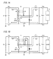
- the DC/DC converting circuit includes: a switching element S1 in which switching operation is performed at high frequency; a transformer T1 including a primary winding N1 and a secondary winding N2, the power-supply voltage of the DC power supply E1 being applied to the primary winding N1 via the switching element S1; a diode (a rectifying element) D1 that is connected in series to the secondary winding N2 of the transformer T1; and a smoothing capacitor (a first capacitor) C1.
- the power supply device includes a capacitor (a second capacitor) C2.
- a capacitor (a second capacitor) C2 Both ends of a series circuit constituted by the secondary winding N2 of the transformer T1 and the diode D1 are connected via the first and second capacitors C1, C2 to a circuit element (the switching element S1) in a closed circuit, which includes the DC power supply E1, the primary winding N1 of the transformer T1 and the switching element S1.
- both ends of the series circuit constituted by the secondary winding N2 of the transformer T1 and the diode D1 are connected to a load X via an inductor L1 serving as a filter.
- the primary winding N1 of the transformer T1, the first capacitor C1, the secondary winding N2 of the transformer T1, and an input side terminal of the diode D1 are connected in series in that order.
- One end of the switching element S1 is connected to a connecting point "a" of one end of the primary winding N1 of the transformer T1 and the first capacitor C1.
- One end of the inductor L1 is connected to a connecting point "b" of the first capacitor C1 and the secondary winding N2 of the transformer T1.
- the second capacitor C2 is connected between the other end of the switching element S1 and an output side terminal of the diode D1.
- the other end of the primary winding N1 of the transformer T1 is connected to a positive electrode of the DC power supply E1.
- a connecting point of the switching element S1 and the second capacitor C2 is connected to a negative electrode of the DC power supply E1.
- the load X is connected between the other end of the inductor L1 and a connecting point "c" of the diode D1 and the second capacitor C2, via output terminals TO2, TO1.
- the other end of the inductor L1 is connected to the output terminal TO2 that is positioned at the low voltage side.
- One end of a capacitor CO serving as a filter is connected to a connecting point of a cathode of the diode D1 and the output terminal TO1 that is positioned at the high voltage side.
- the other end of the capacitor CO is connected to the output terminal TO2.
- the switching element S1 includes a voltage driving type field-effect transistor for example, and the switching operation of the switching element S1 is controlled at high frequency (for example, hundreds kHz) through a drive signal provided from a control circuit (not shown) (PWM control).
- PWM control a control circuit
- the switching control method for the switching element S1 is not limited to PWM control. For example, a method may be adopted in which the switching frequency is changed.
- FIGs. 1A and 1B an input voltage and an input current, which are applied between input terminals TI1, TI2 from the DC power supply E1, are denoted by Vin and IT1, respectively.
- An output voltage, which is applied between the output terminals TO1, TO2, is denoted by Vout. Then, signs of "+" are placed at high voltage sides of the capacitors C1, C2, CO.
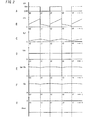
- a waveform in Fig. 2A shows a drive signal for the switching element S1
- a waveform in Fig. 2B shows the input current IT1
- a waveform in Fig. 2C shows an output current IL1
- a waveform in Fig. 2D shows the input voltage Vin
- a waveform in Fig. 2E shows a voltage potential difference Va-Vb between: the connecting point "a" of the first capacitor C1 and the switching element S1; and the connecting point "b" of the secondary winding N2 and the first capacitor C1
- a waveform in Fig. 2F shows an electrical potential (a voltage between both ends of the second capacitor C2) Vc at the connecting point "c" of the second capacitor C2 and the diode D1
- a waveform in Fig. 2G shows the output voltage Vout.
- the energy stored in the transformer T1 is released along a path that passes through the primary winding N1, the first capacitor C1, the secondary winding N2, the diode D1, the second capacitor C2, the DC power supply E1 and the primary winding N1, in that order (see Fig. 1B ). Therefore, a voltage (voltage potential difference Va-Vb) between the both ends of the first capacitor C1, and the voltage Vc between the both ends of the second capacitor C2 are increased.
- the electric charges, which have been stored in the first and second capacitors C1, C2 by charging before the time t t0, are released during an ON period (a period between t0 and t1) when the switching element S1 is in ON.
- the output current IL1 flows along a path that passes through the first capacitor C1, the switching element S1, the second capacitor C2, the capacitor CO, the inductor L1 and the first capacitor C1, in that order, and energy is stored in the inductor L1 (see Fig. 1A ).
- the energy stored in the inductor L1 is released during an OFF period (a period between t1 and t2) when the switching element S1 is in OFF.
- the output current IL1 flows along a path that passes through the inductor L1, the secondary winding N2, the diode D1, the load X and the inductor L1, in that order (see Fig. 1B ).
- the operation of the power supply device according to the present embodiment is different from that of the conventional power supply device shown in Fig. 12 in that the function of the smoothing capacitor C1a in the conventional power supply device is shared by two capacitors (first and second capacitors) C1, C2.
- the amount of the voltage Va-Vb between the both ends of the first capacitor C1 and the amount of the voltage Vc between the both ends of the second capacitor C2 depend on a magnitude relationship between electric capacities thereof (that is, a capacity ratio). In the case of Figs. 2A to 2G , both electric capacities are equal to each other.
- the waveform of the input current IT1 shown in Fig. 2B instantaneously changes in synchronization with the switching operation of the switching element S1.
- the change rate of the input current IT1 depends on the substantive turn ratio of the transformer T1.
- the substantive turn ratio of the transformer T1 is a value obtained by dividing a sum of the number of turns in the primary winding N1 and the number of turns in the secondary winding N2 by the number of turns in the primary winding N1.
- the turn ratio is set so as to be equal to or less than 3, and, more preferably, so as to be equal to or less than 2.
- the turn ratio is properly selected depending on the type of the load X.
- Figs. 1 and 5 because the primary and secondary windings N1, N2 of the transformer T1 are connected in series, when the switching element S1 is turned ON, the current flows through the primary winding N1 as the current pathway, and then when the switching element S1 is turned OFF, the current flows through the primary and secondary windings N1, N2 as the current pathway.
- the substantive turn ratio is a value obtained by dividing a sum of the number of turns in the primary winding N1 and the number of turns in the secondary winding N2 by the number of turns in the primary winding N1.
- the substantive turn ratio is a value obtained by dividing the number of turns in the secondary winding N2 by the number of turns in the primary winding N1, and in this case, preferably, the substantive turn ratio is set so as to be equal to or less than 3.
- the characteristic operation in the present embodiment that is, the operation in the case where electric leakage (earth fault or supply fault) is occurred will be explained below.
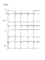
- the operation is explained referring to a time chart in Fig. 4 , in the case where the earth fault is occurred at the output terminal TO2 that is positioned at a low voltage side.
- the conventional power supply device when the earth fault is occurred at the output terminal TO2a of the low voltage side, electric charges, which have been stored in the capacitor COa serving as a filter by charging, are released to ground via the input terminal, and therefore, current leakage (earth fault current) flows.
- the second capacitor C2 is inserted between a high voltage side terminal of the capacitor CO and the input terminal TI1, and then the input side connected to the DC power supply E1 is galvanically separated from the output side connected to the load X by the second capacitor C2. Therefore, the earth fault current does not continually flow. Also in this case, even if the switching operation of the switching element S1 is continued by the control circuit, the power supply device has no problem in particular.
- the power supply device of the present embodiment can reduce the current leakage flowing to circuit, when electric leakage (earth fault or supply fault) is occurred. As a result, the power supply device can prevent problems (the circuit's malfunction or the like) associated with the electric leakage.
- the output voltage Vout applied to the output terminal TO1 of the high voltage side can be set so as to be closer to the ground level.
- a power supply device is characterized in that a resistor R1 is connected in parallel to the second capacitor C2, in that a smoothing capacitor CI is connected in parallel to the input terminals TI1, TI2, and in the configuration of a control circuit CN.
- the other constituent elements are similar to those of First Embodiment. Therefore, such elements are assigned with same reference numerals and the explanation thereof is properly omitted.
- the load X in the present embodiment is a lighting load that includes a series circuit or a series-parallel circuit of a plurality of solid-state light emitting elements (such as light emitting diodes, or organic electroluminescence elements).
- the power supply device corresponds to a lighting device that lights the lighting load.
- the control circuit CN in the present embodiment includes: a differential amplifier circuit having an operational amplifier AMP2, capacitors C13, C14 and resistors R13 to R16; and an error operational circuit having an operational amplifier AMP1, a capacitor C12 and a resistor R12.
- the differential amplifier circuit amplifies a voltage (a voltage proportional to a current value of the output current) between both ends of a sense resistor R2 which is inserted between the output terminal TO1 of the high voltage side and the second capacitor C2, and outputs the amplified voltage to the error operational circuit.
- the error operational circuit amplifies a difference between the amplified output voltage of the differential amplifier circuit and a reference voltage Vref2.
- the control circuit CN further includes a comparator CMP2 that compares the output of the error operational circuit with a reference oscillation signal output from an oscillating circuit OSC1.
- a comparator CMP2 that compares the output of the error operational circuit with a reference oscillation signal output from an oscillating circuit OSC1.
- an output of the comparator CMP2 is at a high level, when the output voltage of the error operational circuit exceeds a signal voltage of the reference oscillation signal.
- the output of the comparator CMP2 is at a low level, when the output voltage of the error operational circuit is equal to or less than the signal voltage of the reference oscillation signal.
- the output of the comparator CMP2 is input to an AND-circuit (AND-gate) AND1.
- the control circuit CN further includes a no-load/short-circuit protection circuit that protects circuit.
- the no-load/short-circuit protection circuit detects: a no-load condition (opened condition) in which the load X is not connected to the output terminals TO1, TO2; and a condition in which short-circuit is generated between the output terminals TO1, TO2.
- the no-load/short-circuit protection circuit includes: an inverting amplifier circuit having an operational amplifier AMP3, a capacitor C15, and resistors R17 to R19; three comparators CMP3, CMP4, CMP5; two timers TM1, TM2; and a NOR-circuit (NOR-gate) NOR1.
- the inverting amplifier circuit inverts and amplifies the output voltage Vout applied to the load X to output into the comparators CMP3, CMP4, CMP5.
- the comparator CMP5 compares the output voltage of the inverting amplifier circuit with a reference voltage Vref5. Then, the output of the comparator CMP5 is at a low level, when the output voltage of the inverting amplifier circuit exceeds the reference voltage Vref5 in the case where the power supply device is in the no-load condition. The output of the comparator CMP5 is at a high level, when the output voltage of the inverting amplifier circuit is equal to or less than the reference voltage Vref5 in the case where the power supply device is not in the no-load condition.
- the outputs of the other two comparators CMP3, CMP4 are at low levels, when the output voltage of the inverting amplifier circuit is within a normal range between two reference voltages Vref3, Vref4 (in this case, Vref5 > Vref4 > Vref3). Then, one of those outputs is at high levels, when the output voltage of the inverting amplifier circuit is out of the normal range.
- the respective timers (time-delay circuits) TM1, TM2 are connected to the output terminals of the comparators CMP3, CMP4.
- the timers TM1, TM2 are activated, and start measuring predetermined times (e.g., 100ms) as count values, respectively.
- predetermined times e.g. 100ms
- the count values in the timers TM1, TM2 are reset and then the outputs are kept at the low levels.
- the outputs of the timers TM1, TM2 are changed to the high levels.
- the output of the NOR-gate NOR1 is kept at the high level, when the output voltage of the inverting amplifier circuit is higher than the low reference voltage Vref3 and is lower than the high reference voltage Vref4.
- the output of the NOR-gate NOR1 is changed to the low level, when the condition that the output voltage of the inverting amplifier circuit is equal to or less than the low reference voltage Vref3 or the condition that the output voltage of the inverting amplifier circuit is equal to or more than the high reference voltage Vref4 is continued over the predetermined time.
- control circuit CN includes an electric leakage detecting circuit.
- This electric leakage detecting circuit includes: a filter circuit (an integrating circuit) having a resistor R11 and a capacitor C11; a comparator CMP1; a time-delay circuit SS1; an AND-circuit (AND-gate) AND2; a zener diode Z11; and the like.
- the comparator CMP1 compares the voltage Vc between both ends of the second capacitor C2, input via the filter circuit, with a reference voltage Vref1. Then, the output of the comparator CMP1 is at the high level, when the voltage Vc is equal to or less than the reference voltage Vref1.
- the output of the comparator CMP1 is at the low level, when the voltage Vc exceeds the reference voltage Vref1.
- the zener diode Z11 is connected to a minus terminal of the comparator CMP1, and is connected in parallel to the filter circuit.
- the zener diode Z11 prevents too much voltage, which exceeds a zener voltage, from being input to the minus terminal.
- the AND-gate AND2 operates a logical AND of the output of the comparator CMP1 and the output of the time-delay circuit SS1, and outputs to the AND-gate AND1. That is, when a period, during which the output of the comparator CMP1 is continually kept at the low level, exceeds a delay time (e.g., 1ms), the output of the time-delay circuit SS1 is changed from the high level to the low level. Then, when the period is less than the delay time, the output of the time-delay circuit SS1 is kept at the high level. When the power supply from the DC power supply E1 is stopped, the output of the time-delay circuit SS1 is reset.
- a delay time e.g. 1ms
- the output of the time-delay circuit SS1 is kept at the high level.
- the output of the time-delay circuit SS1 may be changed from the high level to the low level, when the condition that the output of the comparator CMP1 is changed from the high level to the low level is repeatedly occurred over a predetermined time (e.g., 1ms).
- the control circuit CN switches the switching element S1 at a frequency that is equal to an oscillation frequency of the reference oscillation signal, and adjusts an ON-period for the switching element S1 so that the output current (the load current) corresponds to a target value determined by the reference voltage Vref2.
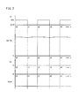
- FIG. 6 shows a time chart in the case where the resistor R2, connected in parallel to the second capacitor C2, has a relatively-small resistance value (e.g., 100 ⁇ or less). Because the resistor R2 is connected in parallel to the second capacitor C2, the voltage Vc between both ends of the second capacitor C2 becomes substantively zero, as shown in Fig. 6 .
- the control circuit CN halts the switching operation of the switching element S1 when electric leakage is occurred, thereby deactivating the power supply device (the lighting device). Therefore, the power supply device (the lighting device) can prevent problems from arising due to continuous flow of current leakage.
- the power supply device the lighting device
- a current continually flows via the resistor R1. In this case, because this current is limited by the resistor R1, an effect on circuit is reduced.
- the control circuit CN may continue to control the switching operation of the switching element S1, without need for detection of electric leakage in the electric leakage detecting circuit.
- the reference voltage Vref1 may be set so as to be higher than a voltage drop (a voltage between both ends) in the sense resistor R2 when electric leakage is occurred, while the resistance value of the sense resistor R2 is set so as to be less than that of the resistor R1 (e.g., R2:0.15 ⁇ , R1:4.7 ⁇ ).
- the reference voltage Vref1 used in the electric leakage detecting circuit when earth fault is occurred at the output terminal TO2, is set to an appropriate value, upon request of the size of the earth fault current at which the power supply device (the lighting device) is deactivated.
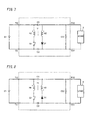
- the main circuits according to First and Second Embodiments may include circuit configurations as shown in Figs. 7 to 9 .
- one end of the primary winding N1 of the transformer T1 is connected to one end of the secondary winding N2 of the transformer T1 via the first capacitor C1.
- One end of the second capacitor C2 is connected to the other end of the primary winding N1 via the switching element S1.
- An anode of the diode D1 is connected to the other end of the secondary winding N2, and a cathode of the diode D1 is connected to the other end of the second capacitor C2.
- a circuit configuration shown in Fig. 8 is similar to the circuit configuration shown in Fig. 7 except that the polarity of the secondary winding N2 of the transformer T1 and a connection direction of the diode D1 are in reverse.
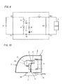
- a circuit configuration shown in Fig. 9 is similar to the circuit configuration shown in Fig. 8 except that the switching element S1 is inserted between the primary winding N1 and the input terminal TI2 of the high voltage side, and the inductor L1 serving as a filter is added.
- the switching element S1 is not limited to a field-effect transistor, and another semiconductor switching element may be adopted.
- a rectifying element except the diode D1 may be adopted.
- the control circuit CN of the present embodiment controls the output current to become constant, using proportional-integral control performed by the error operational circuit, and a method for controlling the output current is not limited to that. Further, the control circuit CN may be constituted by a microcomputer, and a feedback control can be also performed digitally. In addition, the control circuit CN may control the output voltage to become a predetermined value, as substitute for the constant current control.
- Fig. 10 shows a lighting fixture according to the invention
- Fig. 11 shows a vehicle according to the invention
- the lighting fixture A of the present embodiment is a headlight of a vehicle B, such as a car, and includes the power supply device (the lighting device) 1 explained in First or Second Embodiment, a lighting load X, a fixture body 2, a cover 3, an optical unit 4, a radiator plate 5 and the like.
- the fixture body 2 has a box-shape, a front surface of which opens.
- the radiator plate 5 is fixed to a back surface of the fixture body 2 (that is, the bottom surface of the box-shape).
- the lighting load X is attached to the radiator plate 5.
- the optical unit 4 includes a hemispherical lens 40, a reflecting member 41 made of a parabolic mirror, and the like. Light from the lighting load X is emitted effectively through the opening front surface of the fixture body 2.
- the cover 3 is formed of translucent material, such as silica glass or acrylic resin, into a box-shape, the rear of which opens. The cover 3 is attached to the fixture body 2 so as to cover the opening front surface thereof.
- the lighting device 1 includes a printed-wiring board (not shown) on which circuit components constituting the circuit explained in First or Second Embodiment are mounted, and a metallic case 10 that houses the printed-wiring board.
- the case 10 is attached to the outer bottom surface of the fixture body 2, and an electric wire 11 led out from the top surface of the case 10 is connected to the lighting load X.
- the lighting device 1 is connected to a battery (the DC power supply E1), which is installed in the vehicle B, through a power harness 12.
- a negative electrode of the battery is connected to the car body (so-called "body earth”).
- Metallic components (e.g., the radiator plate 5, the case 10, and the like) of the lighting fixture A may be also electrically connected to the car body.
- the radiator plate 5 may be also electrically connected to the case 10 for the purpose of protection against noise or the like. Therefore, there is the fear that a conducting body of the electric wire 11 makes contact with the metallic components of the lighting fixture A or the car body and earth fault is occurred at the output terminal TO1 or TO2 of the lighting device 1, when the conducting body is exposed due to deterioration of a trunking of the electric wire 11 or the like.
- the lighting fixture A according to the present embodiment even when earth fault is occurred, the lighting device 1 is deactivated or the output current is controlled, thereby preventing an accident caused by earth fault current.
- the lighting fixture A according to the present embodiment can be used not only as the headlight of the vehicle B but also as various light fixtures, such as a taillight of the vehicle B, an interior light of the vehicle B, a road light and a room light.
Landscapes
- Engineering & Computer Science (AREA)
- Power Engineering (AREA)
- General Engineering & Computer Science (AREA)
- Circuit Arrangement For Electric Light Sources In General (AREA)
- Dc-Dc Converters (AREA)
Applications Claiming Priority (1)
| Application Number | Priority Date | Filing Date | Title |
|---|---|---|---|
| JP2012163846A JP6008279B2 (ja) | 2012-07-24 | 2012-07-24 | 電源装置、点灯装置およびそれを用いた照明器具並びに車両 |
Publications (3)
| Publication Number | Publication Date |
|---|---|
| EP2690771A2 true EP2690771A2 (fr) | 2014-01-29 |
| EP2690771A3 EP2690771A3 (fr) | 2017-11-29 |
| EP2690771B1 EP2690771B1 (fr) | 2019-12-18 |
Family
ID=48747358
Family Applications (1)
| Application Number | Title | Priority Date | Filing Date |
|---|---|---|---|
| EP13173789.2A Active EP2690771B1 (fr) | 2012-07-24 | 2013-06-26 | Dispositif d'alimentation électrique, dispositif d'éclairage, appareil d'éclairage l'utilisant et véhicule |
Country Status (5)
| Country | Link |
|---|---|
| US (1) | US20140028187A1 (fr) |
| EP (1) | EP2690771B1 (fr) |
| JP (1) | JP6008279B2 (fr) |
| KR (1) | KR101553746B1 (fr) |
| CN (1) | CN103582248B (fr) |
Cited By (2)
| Publication number | Priority date | Publication date | Assignee | Title |
|---|---|---|---|---|
| EP3262901A4 (fr) * | 2015-02-26 | 2018-03-07 | Tridonic GmbH & Co. KG | Dispositif d'actionnement pour un élément d'éclairage |
| CN110035581A (zh) * | 2019-04-22 | 2019-07-19 | 上海芯荃微电子科技有限公司 | 慢计时模块 |
Families Citing this family (6)
| Publication number | Priority date | Publication date | Assignee | Title |
|---|---|---|---|---|
| DE102016111498A1 (de) * | 2015-07-07 | 2017-01-12 | Panasonic Intellectual Property Management Co., Ltd. | Stromversorgungsvorrichtung und beleuchtungskörper |
| JP7334977B2 (ja) * | 2017-04-28 | 2023-08-29 | ブルメスター オーディオシステム ゲーエムベーハー | 信号増幅器回路、電圧変換器およびシステム |
| JP7191767B2 (ja) * | 2019-05-27 | 2022-12-19 | 株式会社東芝 | 電流検出回路 |
| CN114684045A (zh) * | 2020-12-30 | 2022-07-01 | 罗伯特·博世有限公司 | 电源输出装置、故障诊断方法、安全气囊控制器及安全气囊系统 |
| WO2022246805A1 (fr) * | 2021-05-28 | 2022-12-01 | Tridonic Gmbh & Co Kg | Convertisseur à diodes électroluminescentes et dispositif à del |
| US12068687B2 (en) * | 2021-10-15 | 2024-08-20 | Advanced Micro Devices, Inc. | Method to reduce overshoot in a voltage regulating power supply |
Citations (1)
| Publication number | Priority date | Publication date | Assignee | Title |
|---|---|---|---|---|
| JP2002159172A (ja) | 2000-11-15 | 2002-05-31 | Matsushita Electric Works Ltd | 電源装置及び放電灯点灯装置 |
Family Cites Families (17)
| Publication number | Priority date | Publication date | Assignee | Title |
|---|---|---|---|---|
| JPS5855751B2 (ja) * | 1976-01-29 | 1983-12-12 | ソニー株式会社 | 電源回路 |
| US4184197A (en) * | 1977-09-28 | 1980-01-15 | California Institute Of Technology | DC-to-DC switching converter |
| US4257087A (en) * | 1979-04-02 | 1981-03-17 | California Institute Of Technology | DC-to-DC switching converter with zero input and output current ripple and integrated magnetics circuits |
| DE4342590A1 (de) * | 1993-12-14 | 1995-06-22 | Bosch Gmbh Robert | Getaktete Stromversorgung |
| US5583421A (en) * | 1994-08-10 | 1996-12-10 | Hewlett-Packard Company | Sepic converter with transformerless line isolation |
| US6144565A (en) * | 1999-07-20 | 2000-11-07 | Semtech Corporation | Variation on a single-ended primary inductor converter |
| JP4236894B2 (ja) * | 2002-10-08 | 2009-03-11 | 株式会社小糸製作所 | 点灯回路 |
| KR20050050674A (ko) * | 2002-10-16 | 2005-05-31 | 톰슨 라이센싱 에스.에이. | 용량성 연결된 전원 공급기 |
| JP4935499B2 (ja) * | 2007-05-18 | 2012-05-23 | サンケン電気株式会社 | 直流変換装置 |
| US8058861B2 (en) | 2007-06-05 | 2011-11-15 | Bayer Materialscience Ag | Miniature high-voltage power supplies |
| EP2023475B1 (fr) * | 2007-08-04 | 2016-10-12 | SMA Solar Technology AG | Inversion pour une source de tension continue reliée à la terre, en particulier un générateur photovoltaïque |
| JP5149686B2 (ja) * | 2008-04-24 | 2013-02-20 | パナソニック株式会社 | 電力変換装置及びそれを用いた放電灯点灯装置、並びに車両用前照灯装置 |
| JP5265966B2 (ja) * | 2008-05-26 | 2013-08-14 | パナソニック株式会社 | 電源装置および灯具、車両 |
| JP5161040B2 (ja) * | 2008-11-11 | 2013-03-13 | スタンレー電気株式会社 | 車両用灯具の点灯制御装置 |
| JP6016153B2 (ja) * | 2011-05-24 | 2016-10-26 | パナソニックIpマネジメント株式会社 | 電源装置及びそれを用いた灯具並びに車両 |
| CN104254970B (zh) * | 2012-04-27 | 2017-03-08 | 三菱电机株式会社 | Dc/dc转换器、车载设备及充电装置 |
| JP6160955B2 (ja) * | 2013-07-10 | 2017-07-12 | パナソニックIpマネジメント株式会社 | 発光ダイオード駆動装置、それを備えた車両用照明装置および車両 |
-
2012
- 2012-07-24 JP JP2012163846A patent/JP6008279B2/ja active Active
-
2013
- 2013-06-26 EP EP13173789.2A patent/EP2690771B1/fr active Active
- 2013-07-17 US US13/944,150 patent/US20140028187A1/en not_active Abandoned
- 2013-07-23 KR KR1020130086516A patent/KR101553746B1/ko not_active Expired - Fee Related
- 2013-07-24 CN CN201310314882.4A patent/CN103582248B/zh active Active
Patent Citations (1)
| Publication number | Priority date | Publication date | Assignee | Title |
|---|---|---|---|---|
| JP2002159172A (ja) | 2000-11-15 | 2002-05-31 | Matsushita Electric Works Ltd | 電源装置及び放電灯点灯装置 |
Cited By (3)
| Publication number | Priority date | Publication date | Assignee | Title |
|---|---|---|---|---|
| EP3262901A4 (fr) * | 2015-02-26 | 2018-03-07 | Tridonic GmbH & Co. KG | Dispositif d'actionnement pour un élément d'éclairage |
| CN110035581A (zh) * | 2019-04-22 | 2019-07-19 | 上海芯荃微电子科技有限公司 | 慢计时模块 |
| CN110035581B (zh) * | 2019-04-22 | 2023-10-13 | 上海芯荃微电子科技有限公司 | 慢计时模块 |
Also Published As
| Publication number | Publication date |
|---|---|
| CN103582248B (zh) | 2016-02-24 |
| US20140028187A1 (en) | 2014-01-30 |
| JP6008279B2 (ja) | 2016-10-19 |
| EP2690771A3 (fr) | 2017-11-29 |
| KR20140013963A (ko) | 2014-02-05 |
| EP2690771B1 (fr) | 2019-12-18 |
| CN103582248A (zh) | 2014-02-12 |
| KR101553746B1 (ko) | 2015-09-16 |
| JP2014027714A (ja) | 2014-02-06 |
Similar Documents
| Publication | Publication Date | Title |
|---|---|---|
| EP2690771B1 (fr) | Dispositif d'alimentation électrique, dispositif d'éclairage, appareil d'éclairage l'utilisant et véhicule | |
| US9462647B2 (en) | Lighting device, head light and vehicle | |
| JP5265966B2 (ja) | 電源装置および灯具、車両 | |
| US8421424B2 (en) | Current driver circuit | |
| JP4926784B2 (ja) | 発光装置 | |
| EP2528419B1 (fr) | Dispositif de source électrique pour lampe et vehicle le comprenant | |
| US20150180325A1 (en) | Electrolytic capacitor-less ac/dc converter and controlling method thereof | |
| EP2749128B1 (fr) | Circuit d'attaque pour la connexion de diode électroluminescente à un ballast électronique | |
| KR101516566B1 (ko) | 직류전원장치 | |
| ES2901994T3 (es) | Dispositivo de fuente de alimentación ininterrumpida. | |
| JP5874052B2 (ja) | 電源装置、点灯装置、灯具、車両 | |
| JP2011192865A (ja) | 点灯制御装置及び車両用灯具 | |
| KR102365558B1 (ko) | Led 조명등의 잔광제거 장치와, 이를 구비한 led 조명등의 구동장치 및 led 조명장치 | |
| JP5877371B2 (ja) | 電源装置、点灯装置、灯具、及び車両 | |
| JP6332629B2 (ja) | Led電源及びled照明装置 | |
| US10004116B2 (en) | Lighting device, headlight device with the same, and vehicle | |
| KR101243694B1 (ko) | 이종 축전지를 포함하는 전력 저장 장치 및 이를 이용한 태양광 가로등 | |
| WO2013077269A1 (fr) | Dispositif d'alimentation électrique, dispositif d'éclairage, accessoire de lampe et véhicule | |
| KR100855871B1 (ko) | 충전식 전원장치 및 그 제어방법 | |
| EP3487056B1 (fr) | Détection combinée de courant, de tension et de passage par zéro avec drain zéro en attente | |
| JP2013038992A (ja) | スイッチング電源装置 | |
| JP2025183754A (ja) | 双方向dc/dcコンバータユニット及び電源回路 | |
| JP2010283969A (ja) | 充電装置及び照明装置 |
Legal Events
| Date | Code | Title | Description |
|---|---|---|---|
| PUAI | Public reference made under article 153(3) epc to a published international application that has entered the european phase |
Free format text: ORIGINAL CODE: 0009012 |
|
| 17P | Request for examination filed |
Effective date: 20130626 |
|
| AK | Designated contracting states |
Kind code of ref document: A2 Designated state(s): AL AT BE BG CH CY CZ DE DK EE ES FI FR GB GR HR HU IE IS IT LI LT LU LV MC MK MT NL NO PL PT RO RS SE SI SK SM TR |
|
| AX | Request for extension of the european patent |
Extension state: BA ME |
|
| RAP1 | Party data changed (applicant data changed or rights of an application transferred) |
Owner name: PANASONIC INTELLECTUAL PROPERTY MANAGEMENT CO., LT |
|
| PUAL | Search report despatched |
Free format text: ORIGINAL CODE: 0009013 |
|
| AK | Designated contracting states |
Kind code of ref document: A3 Designated state(s): AL AT BE BG CH CY CZ DE DK EE ES FI FR GB GR HR HU IE IS IT LI LT LU LV MC MK MT NL NO PL PT RO RS SE SI SK SM TR |
|
| AX | Request for extension of the european patent |
Extension state: BA ME |
|
| RIC1 | Information provided on ipc code assigned before grant |
Ipc: H02M 1/14 20060101ALI20171020BHEP Ipc: H05B 41/288 20060101ALI20171020BHEP Ipc: H05B 41/28 20060101ALI20171020BHEP Ipc: H02M 3/00 20060101AFI20171020BHEP |
|
| GRAP | Despatch of communication of intention to grant a patent |
Free format text: ORIGINAL CODE: EPIDOSNIGR1 |
|
| STAA | Information on the status of an ep patent application or granted ep patent |
Free format text: STATUS: GRANT OF PATENT IS INTENDED |
|
| RIC1 | Information provided on ipc code assigned before grant |
Ipc: H02M 1/14 20060101ALI20190624BHEP Ipc: H05B 33/08 20060101ALI20190624BHEP Ipc: H02M 3/00 20060101AFI20190624BHEP Ipc: H02M 3/155 20060101ALN20190624BHEP |
|
| RIC1 | Information provided on ipc code assigned before grant |
Ipc: H02M 3/155 20060101ALN20190704BHEP Ipc: H05B 33/08 20060101ALI20190704BHEP Ipc: H02M 3/00 20060101AFI20190704BHEP Ipc: H02M 1/14 20060101ALI20190704BHEP |
|
| INTG | Intention to grant announced |
Effective date: 20190722 |
|
| GRAS | Grant fee paid |
Free format text: ORIGINAL CODE: EPIDOSNIGR3 |
|
| GRAA | (expected) grant |
Free format text: ORIGINAL CODE: 0009210 |
|
| STAA | Information on the status of an ep patent application or granted ep patent |
Free format text: STATUS: THE PATENT HAS BEEN GRANTED |
|
| AK | Designated contracting states |
Kind code of ref document: B1 Designated state(s): AL AT BE BG CH CY CZ DE DK EE ES FI FR GB GR HR HU IE IS IT LI LT LU LV MC MK MT NL NO PL PT RO RS SE SI SK SM TR |
|
| REG | Reference to a national code |
Ref country code: GB Ref legal event code: FG4D |
|
| REG | Reference to a national code |
Ref country code: CH Ref legal event code: EP |
|
| REG | Reference to a national code |
Ref country code: IE Ref legal event code: FG4D |
|
| REG | Reference to a national code |
Ref country code: DE Ref legal event code: R096 Ref document number: 602013064041 Country of ref document: DE |
|
| REG | Reference to a national code |
Ref country code: AT Ref legal event code: REF Ref document number: 1215662 Country of ref document: AT Kind code of ref document: T Effective date: 20200115 |
|
| REG | Reference to a national code |
Ref country code: NL Ref legal event code: MP Effective date: 20191218 |
|
| PG25 | Lapsed in a contracting state [announced via postgrant information from national office to epo] |
Ref country code: BG Free format text: LAPSE BECAUSE OF FAILURE TO SUBMIT A TRANSLATION OF THE DESCRIPTION OR TO PAY THE FEE WITHIN THE PRESCRIBED TIME-LIMIT Effective date: 20200318 Ref country code: FI Free format text: LAPSE BECAUSE OF FAILURE TO SUBMIT A TRANSLATION OF THE DESCRIPTION OR TO PAY THE FEE WITHIN THE PRESCRIBED TIME-LIMIT Effective date: 20191218 Ref country code: LV Free format text: LAPSE BECAUSE OF FAILURE TO SUBMIT A TRANSLATION OF THE DESCRIPTION OR TO PAY THE FEE WITHIN THE PRESCRIBED TIME-LIMIT Effective date: 20191218 Ref country code: SE Free format text: LAPSE BECAUSE OF FAILURE TO SUBMIT A TRANSLATION OF THE DESCRIPTION OR TO PAY THE FEE WITHIN THE PRESCRIBED TIME-LIMIT Effective date: 20191218 Ref country code: NO Free format text: LAPSE BECAUSE OF FAILURE TO SUBMIT A TRANSLATION OF THE DESCRIPTION OR TO PAY THE FEE WITHIN THE PRESCRIBED TIME-LIMIT Effective date: 20200318 Ref country code: GR Free format text: LAPSE BECAUSE OF FAILURE TO SUBMIT A TRANSLATION OF THE DESCRIPTION OR TO PAY THE FEE WITHIN THE PRESCRIBED TIME-LIMIT Effective date: 20200319 Ref country code: LT Free format text: LAPSE BECAUSE OF FAILURE TO SUBMIT A TRANSLATION OF THE DESCRIPTION OR TO PAY THE FEE WITHIN THE PRESCRIBED TIME-LIMIT Effective date: 20191218 |
|
| REG | Reference to a national code |
Ref country code: LT Ref legal event code: MG4D |
|
| PG25 | Lapsed in a contracting state [announced via postgrant information from national office to epo] |
Ref country code: HR Free format text: LAPSE BECAUSE OF FAILURE TO SUBMIT A TRANSLATION OF THE DESCRIPTION OR TO PAY THE FEE WITHIN THE PRESCRIBED TIME-LIMIT Effective date: 20191218 Ref country code: RS Free format text: LAPSE BECAUSE OF FAILURE TO SUBMIT A TRANSLATION OF THE DESCRIPTION OR TO PAY THE FEE WITHIN THE PRESCRIBED TIME-LIMIT Effective date: 20191218 |
|
| PG25 | Lapsed in a contracting state [announced via postgrant information from national office to epo] |
Ref country code: AL Free format text: LAPSE BECAUSE OF FAILURE TO SUBMIT A TRANSLATION OF THE DESCRIPTION OR TO PAY THE FEE WITHIN THE PRESCRIBED TIME-LIMIT Effective date: 20191218 |
|
| PG25 | Lapsed in a contracting state [announced via postgrant information from national office to epo] |
Ref country code: EE Free format text: LAPSE BECAUSE OF FAILURE TO SUBMIT A TRANSLATION OF THE DESCRIPTION OR TO PAY THE FEE WITHIN THE PRESCRIBED TIME-LIMIT Effective date: 20191218 Ref country code: PT Free format text: LAPSE BECAUSE OF FAILURE TO SUBMIT A TRANSLATION OF THE DESCRIPTION OR TO PAY THE FEE WITHIN THE PRESCRIBED TIME-LIMIT Effective date: 20200513 Ref country code: NL Free format text: LAPSE BECAUSE OF FAILURE TO SUBMIT A TRANSLATION OF THE DESCRIPTION OR TO PAY THE FEE WITHIN THE PRESCRIBED TIME-LIMIT Effective date: 20191218 Ref country code: RO Free format text: LAPSE BECAUSE OF FAILURE TO SUBMIT A TRANSLATION OF THE DESCRIPTION OR TO PAY THE FEE WITHIN THE PRESCRIBED TIME-LIMIT Effective date: 20191218 Ref country code: CZ Free format text: LAPSE BECAUSE OF FAILURE TO SUBMIT A TRANSLATION OF THE DESCRIPTION OR TO PAY THE FEE WITHIN THE PRESCRIBED TIME-LIMIT Effective date: 20191218 |
|
| PG25 | Lapsed in a contracting state [announced via postgrant information from national office to epo] |
Ref country code: SM Free format text: LAPSE BECAUSE OF FAILURE TO SUBMIT A TRANSLATION OF THE DESCRIPTION OR TO PAY THE FEE WITHIN THE PRESCRIBED TIME-LIMIT Effective date: 20191218 Ref country code: IS Free format text: LAPSE BECAUSE OF FAILURE TO SUBMIT A TRANSLATION OF THE DESCRIPTION OR TO PAY THE FEE WITHIN THE PRESCRIBED TIME-LIMIT Effective date: 20200418 Ref country code: SK Free format text: LAPSE BECAUSE OF FAILURE TO SUBMIT A TRANSLATION OF THE DESCRIPTION OR TO PAY THE FEE WITHIN THE PRESCRIBED TIME-LIMIT Effective date: 20191218 |
|
| REG | Reference to a national code |
Ref country code: DE Ref legal event code: R097 Ref document number: 602013064041 Country of ref document: DE |
|
| REG | Reference to a national code |
Ref country code: AT Ref legal event code: MK05 Ref document number: 1215662 Country of ref document: AT Kind code of ref document: T Effective date: 20191218 |
|
| PLBE | No opposition filed within time limit |
Free format text: ORIGINAL CODE: 0009261 |
|
| STAA | Information on the status of an ep patent application or granted ep patent |
Free format text: STATUS: NO OPPOSITION FILED WITHIN TIME LIMIT |
|
| PG25 | Lapsed in a contracting state [announced via postgrant information from national office to epo] |
Ref country code: DK Free format text: LAPSE BECAUSE OF FAILURE TO SUBMIT A TRANSLATION OF THE DESCRIPTION OR TO PAY THE FEE WITHIN THE PRESCRIBED TIME-LIMIT Effective date: 20191218 Ref country code: ES Free format text: LAPSE BECAUSE OF FAILURE TO SUBMIT A TRANSLATION OF THE DESCRIPTION OR TO PAY THE FEE WITHIN THE PRESCRIBED TIME-LIMIT Effective date: 20191218 |
|
| 26N | No opposition filed |
Effective date: 20200921 |
|
| PG25 | Lapsed in a contracting state [announced via postgrant information from national office to epo] |
Ref country code: AT Free format text: LAPSE BECAUSE OF FAILURE TO SUBMIT A TRANSLATION OF THE DESCRIPTION OR TO PAY THE FEE WITHIN THE PRESCRIBED TIME-LIMIT Effective date: 20191218 Ref country code: SI Free format text: LAPSE BECAUSE OF FAILURE TO SUBMIT A TRANSLATION OF THE DESCRIPTION OR TO PAY THE FEE WITHIN THE PRESCRIBED TIME-LIMIT Effective date: 20191218 |
|
| PG25 | Lapsed in a contracting state [announced via postgrant information from national office to epo] |
Ref country code: IT Free format text: LAPSE BECAUSE OF FAILURE TO SUBMIT A TRANSLATION OF THE DESCRIPTION OR TO PAY THE FEE WITHIN THE PRESCRIBED TIME-LIMIT Effective date: 20191218 Ref country code: MC Free format text: LAPSE BECAUSE OF FAILURE TO SUBMIT A TRANSLATION OF THE DESCRIPTION OR TO PAY THE FEE WITHIN THE PRESCRIBED TIME-LIMIT Effective date: 20191218 |
|
| REG | Reference to a national code |
Ref country code: CH Ref legal event code: PL |
|
| PG25 | Lapsed in a contracting state [announced via postgrant information from national office to epo] |
Ref country code: PL Free format text: LAPSE BECAUSE OF FAILURE TO SUBMIT A TRANSLATION OF THE DESCRIPTION OR TO PAY THE FEE WITHIN THE PRESCRIBED TIME-LIMIT Effective date: 20191218 |
|
| GBPC | Gb: european patent ceased through non-payment of renewal fee |
Effective date: 20200626 |
|
| PG25 | Lapsed in a contracting state [announced via postgrant information from national office to epo] |
Ref country code: LU Free format text: LAPSE BECAUSE OF NON-PAYMENT OF DUE FEES Effective date: 20200626 |
|
| REG | Reference to a national code |
Ref country code: BE Ref legal event code: MM Effective date: 20200630 |
|
| PG25 | Lapsed in a contracting state [announced via postgrant information from national office to epo] |
Ref country code: LI Free format text: LAPSE BECAUSE OF NON-PAYMENT OF DUE FEES Effective date: 20200630 Ref country code: IE Free format text: LAPSE BECAUSE OF NON-PAYMENT OF DUE FEES Effective date: 20200626 Ref country code: CH Free format text: LAPSE BECAUSE OF NON-PAYMENT OF DUE FEES Effective date: 20200630 Ref country code: FR Free format text: LAPSE BECAUSE OF NON-PAYMENT OF DUE FEES Effective date: 20200630 Ref country code: GB Free format text: LAPSE BECAUSE OF NON-PAYMENT OF DUE FEES Effective date: 20200626 |
|
| PG25 | Lapsed in a contracting state [announced via postgrant information from national office to epo] |
Ref country code: BE Free format text: LAPSE BECAUSE OF NON-PAYMENT OF DUE FEES Effective date: 20200630 |
|
| PG25 | Lapsed in a contracting state [announced via postgrant information from national office to epo] |
Ref country code: TR Free format text: LAPSE BECAUSE OF FAILURE TO SUBMIT A TRANSLATION OF THE DESCRIPTION OR TO PAY THE FEE WITHIN THE PRESCRIBED TIME-LIMIT Effective date: 20191218 Ref country code: MT Free format text: LAPSE BECAUSE OF FAILURE TO SUBMIT A TRANSLATION OF THE DESCRIPTION OR TO PAY THE FEE WITHIN THE PRESCRIBED TIME-LIMIT Effective date: 20191218 Ref country code: CY Free format text: LAPSE BECAUSE OF FAILURE TO SUBMIT A TRANSLATION OF THE DESCRIPTION OR TO PAY THE FEE WITHIN THE PRESCRIBED TIME-LIMIT Effective date: 20191218 |
|
| PG25 | Lapsed in a contracting state [announced via postgrant information from national office to epo] |
Ref country code: MK Free format text: LAPSE BECAUSE OF FAILURE TO SUBMIT A TRANSLATION OF THE DESCRIPTION OR TO PAY THE FEE WITHIN THE PRESCRIBED TIME-LIMIT Effective date: 20191218 |
|
| PGFP | Annual fee paid to national office [announced via postgrant information from national office to epo] |
Ref country code: DE Payment date: 20250618 Year of fee payment: 13 |