EP2693639A1 - Kaskodenhalbleiterbauelemente - Google Patents
Kaskodenhalbleiterbauelemente Download PDFInfo
- Publication number
- EP2693639A1 EP2693639A1 EP12178518.2A EP12178518A EP2693639A1 EP 2693639 A1 EP2693639 A1 EP 2693639A1 EP 12178518 A EP12178518 A EP 12178518A EP 2693639 A1 EP2693639 A1 EP 2693639A1
- Authority
- EP
- European Patent Office
- Prior art keywords
- circuit
- gan
- gate
- transistor
- gallium nitride
- Prior art date
- Legal status (The legal status is an assumption and is not a legal conclusion. Google has not performed a legal analysis and makes no representation as to the accuracy of the status listed.)
- Granted
Links
Images
Classifications
-
- H—ELECTRICITY
- H03—ELECTRONIC CIRCUITRY
- H03K—PULSE TECHNIQUE
- H03K17/00—Electronic switching or gating, i.e. not by contact-making and –breaking
- H03K17/08—Modifications for protecting switching circuit against overcurrent or overvoltage
- H03K17/081—Modifications for protecting switching circuit against overcurrent or overvoltage without feedback from the output circuit to the control circuit
- H03K17/0812—Modifications for protecting switching circuit against overcurrent or overvoltage without feedback from the output circuit to the control circuit by measures taken in the control circuit
- H03K17/08122—Modifications for protecting switching circuit against overcurrent or overvoltage without feedback from the output circuit to the control circuit by measures taken in the control circuit in field-effect transistor switches
-
- H—ELECTRICITY
- H10—SEMICONDUCTOR DEVICES; ELECTRIC SOLID-STATE DEVICES NOT OTHERWISE PROVIDED FOR
- H10D—INORGANIC ELECTRIC SEMICONDUCTOR DEVICES
- H10D84/00—Integrated devices formed in or on semiconductor substrates that comprise only semiconducting layers, e.g. on Si wafers or on GaAs-on-Si wafers
-
- H—ELECTRICITY
- H03—ELECTRONIC CIRCUITRY
- H03K—PULSE TECHNIQUE
- H03K17/00—Electronic switching or gating, i.e. not by contact-making and –breaking
- H03K17/10—Modifications for increasing the maximum permissible switched voltage
- H03K17/102—Modifications for increasing the maximum permissible switched voltage in field-effect transistor switches
-
- H—ELECTRICITY
- H03—ELECTRONIC CIRCUITRY
- H03K—PULSE TECHNIQUE
- H03K17/00—Electronic switching or gating, i.e. not by contact-making and –breaking
- H03K17/51—Electronic switching or gating, i.e. not by contact-making and –breaking characterised by the components used
- H03K17/56—Electronic switching or gating, i.e. not by contact-making and –breaking characterised by the components used by the use, as active elements, of semiconductor devices
- H03K17/567—Circuits characterised by the use of more than one type of semiconductor device, e.g. BIMOS, composite devices such as IGBT
-
- H—ELECTRICITY
- H03—ELECTRONIC CIRCUITRY
- H03K—PULSE TECHNIQUE
- H03K17/00—Electronic switching or gating, i.e. not by contact-making and –breaking
- H03K17/51—Electronic switching or gating, i.e. not by contact-making and –breaking characterised by the components used
- H03K17/56—Electronic switching or gating, i.e. not by contact-making and –breaking characterised by the components used by the use, as active elements, of semiconductor devices
- H03K17/687—Electronic switching or gating, i.e. not by contact-making and –breaking characterised by the components used by the use, as active elements, of semiconductor devices the devices being field-effect transistors
- H03K2017/6875—Electronic switching or gating, i.e. not by contact-making and –breaking characterised by the components used by the use, as active elements, of semiconductor devices the devices being field-effect transistors using self-conductive, depletion FETs
Definitions
- This invention relates to cascoded semiconductor devices. It relates in particular to depletion mode transistors, such as gallium nitride (GaN) transistors (e.g. GaN high electron mobility transistors (HEMTs)), or silicon carbide (SiC) MOSFETs.
- GaN gallium nitride
- HEMTs high electron mobility transistors
- SiC silicon carbide
- the invention is of particular interest for GaN power transistors.
- Basic GaN power semiconductors are depletion mode (normally-on) devices. Attempts to introduce additional layers in the layer stack of the power semiconductor to make the device normally-off come together with device performance penalties. Therefore, cascoding high-voltage GaN switches with conventional low-voltage silicon MOSFETs is a viable option to combine the advantages of Silicon and GaN power devices.
- Another advantage of a cascoded switch is the fact that existing standard gate drivers can be used as the device DC characteristics are mainly defined by the silicon MOSFET. Therefore the device can be used as a direct replacement for silicon MOSFETs or IGBTs.
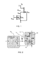
- Figure 1 shows a well-known approach of a series connection of a normally-on gallium nitride transistor (M GaN ) and a normally-off silicon MOSFET transistor (M Si ) power switch in a cascode configuration.
- M GaN normally-on gallium nitride transistor
- M Si normally-off silicon MOSFET transistor
- a cascode transistor circuit comprising:
- the invention provides a control circuit which makes use of a bootstrap arrangement to allow an active control of both power switches of a cascode circuit using a single gate driver, since the gates are connected by the bootstrap circuit (capacitor and diode).
- the diode is used to charge the capacitor when the cascode (silicon) MOSFET is turned on and blocks the voltage to generate a negative voltage at the gate of the gallium nitride or silicon carbide FET when the device turns off.
- the diode can comprise a discrete Schottky or pn-junction diode connected outside the package of the cascode structure.
- the diode can be integrated either on the GaN or SiC FET chip or the Si chip of the cascode transistor. In this case bond wires are used to establish the necessary interconnects between the Si chip and the GaN or SiC FET chip.
- a Schottky diode is integrated on the GaN or SiC FET chip.
- GaN technology is a lateral device technology which allows integration of additional circuitry.
- the diode needs to be designed only for the average gate current of the GaN or SiC FET. It is therefore a small diode structure in comparison to the GaN or SiC FET.
- the GaN or SiC FET preferably comprises a high voltage power semiconductor, such as a GaN high electron mobility transistor (HEMT).
- HEMT GaN high electron mobility transistor
- GaN transistors are considered to be most attractive for operating voltages in the range of 200V up to 1200V.
- GaN transistors can generally be used for a very broad range of applications and power levels. For example, they can be used in high performance, high frequency power supplies in which high efficiency and power density is achieved at a premium.
- the silicon MOSFET transistor preferably comprises a low voltage power MOSFET (typically V DS ⁇ 30V) in a trench MOS technology.
- the MOSFET is scaled in relation to the GaN or SiC FET and can have an on-state resistance (R DS ( on )) which is a small fraction of the on-state resistance of the GaN or SiC transistor.
- the bootstrap capacitor preferably comprises a discrete capacitor next to the cascode switch device. It can be a low voltage rated capacitor as it will be charged to the driver supply voltage.
- the capacitance is preferably at least the same size as the input capacitance (C ISS ) of the GaN or SiC FET, or more preferably several times larger.
- the invention also provides a circuit arrangement comprising:
- the cascode transistor circuit enables standard gate drivers to be used.
- the invention provides a cascoded power semiconductor circuit. Emerging new power switches based on GaN and SiC insulated gate devices (such as MOSFETs) often have depletion-mode (normally on) behaviour. Hence, they cannot be used in most power converter applications because they are turned on if the gate is unbiased and hence cause undesired fault conditions in the application.
- One common solution to realize an inherently safe power switch is to combine a conventional enhancement-mode (normally-off) power switch with these depletion mode (normally-on) power switches in a cascode configuration.
- the invention provides a circuit which makes use of a bootstrap arrangement to allow an active control of both power switches of a cascode circuit using a single gate driver.
- a bootstrap controlled cascode circuit comprising an example of the invention is shown in Figure 2 .
- a standard gate driver 10 with a single gate output, a bootstrap circuit 12, 14, a cascode connected normally on transistor 16 (corresponding to M GaN in Figure 1 ) and a normally off transistor 18 (corresponding to M Si in Figure 1 ).
- the normally on transistor is described as a GaN HEMT.
- the cascode circuit comprises the two transistors in series (i.e. with their drain-source channels in series) between power lines.
- the cascode circuit has external connections to the gate of the normally on transistor 16 (node GH) and to the gate of the normally off transistor 18 (node GM).
- the bootstrap circuit comprises a capacitor 12 between the gate driver circuit output and the gate of the transistor 16, so that this capacitor is between the gates of the two transistors, and a bootstrap diode 14 between the gate of the transistor 16 and the source of the transistor 18.
- the bootstrap diode 14 can in practice be integrated with the circuit of the GaN transistor in which case only one additional bootstrap capacitor is required outside the cascode circuit package.
- the cascode circuit package is shown as a grey area in Figure 2 . It is a dual die solution with a Si chip (the silicon MOSFET 18) and a GaN chip (GaN transistor 16 and diode 14). In the example shown, the diode is a separate device integrated on the same chip as the GaN transistor (and therefore in the grey area), but it can be a discrete component outside the cascode switch package.
- the normally off transistor is a silicon MOSFET
- the gate driver is a conventional MOSFET gate driver.
- the normally on transistor is a GaN HEMT transistor. As mentioned above, it can instead be a SiC MOSFET.
- the bootstrap capacitor 12 will be charged by the gate driver to the MOSFET on-state voltage.
- the node voltages of GM and GH will change in the same manner as a result of the bootstrap capacitor.
- the node between the series connection of the transistors is shown as DM (the drain of the MOSFET).
- the voltage at GM equals the MOSFET on state voltage and the voltage at GH is about zero. While turning off the MOSFET 18, the GM node voltage will decrease and node GH will become negative. Both devices are controlled by the gate driver simultaneously.
- the GaN device will turn off first and takes the full drain source voltage. During the increase of the overall drain voltage the MOSFET is still turned on and discharges the node DM before it becomes a floating node.
- the circuit aims to address one or more of the problems of known cascode circuits, namely:
- the MOSFET M Si is controlled by a gate driver.
- V t the threshold voltage level
- M Si stops conducting current while M GaN is still turned on.
- the drain voltage at node DM starts increasing.
- the M Si drain-source voltage equals the M GaN source-gate voltage.
- an increase of V DM implies a decrease of M GaN gate-source voltage as well.
- the GaN/SiC device turns off passively when its source-gate voltage equals its V t . If the cascode is considered to be ideal, the M Si drain-source voltage would then be limited to the threshold voltage V t of M GaN .
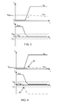
- Figure 3 shows the turn off behavior of the standard cascode circuit of Figure 1 .
- the plots shown are the gate signal V GM for the silicon MOSFET, the gate signal V GH for the GaN transistor, the GaN drain signal V D (the high power rail) and the MOSFET drain signal V DM which equates to the drain-source voltage across the MOSFET These are all shown in Figure 1 .
- the threshold voltages for the silicon MOSFET and for the GaN transistor are shown as V tM and V tH ..
- the plots show the switch off characteristics.
- Figure 4 shows the behavior of the bootstrap controlled cascode according to the circuit shown in Figure 2 .
- the plots shown are the MOSFET gate signal V GM , the GaN gate signal V GH , the MOSFET drain signal V DM which equates to the drain-source voltage across the MOSFET and the GaN drain signal V D (the high power rail). These are all shown in Figure 2 .
- the threshold voltages for the silicon MOSFET and for the GaN transistor are again shown as V tM and V tH .
- the plots again show the switch off characteristics.
- the voltage at node GH becomes negative at the time shown as 20 and the GaN device turns off first.
- the MOSFET drain voltage peak node DM
- the MOSFET drain voltage does not increase significantly during turn off.
- the diode 14 is thus used to charge the capacitor 12 when the cascode MOSFET is turned on and blocks the voltage to generate a negative voltage at the gate of the GaN transistor when the device turns off.
- the bootstrap controlled cascode offers better controllability of switching speed (by means of dv/dt and di/dt during switching) compared to the standard cascode.
- the input capacitance of switch M GaN (see Figure 1 ) is charged by the drain current during turn off and discharged via the switch M Si during turn on. Hence, no direct control of M GaN is possible via the driver.
- the driver charges and discharges the gates of both switches M GaN and M Si simultaneously.
- the switching speed of M GaN can be adjusted directly by the driver.
- the switch M GaN turns on and off passively in the case of a standard cascode.
- the input capacitance of M GaN is charged and discharged by the device output rather than by a gate driver connected to the input. This leads to an increased effective output capacitance C OSS for drain-source voltages below threshold voltage V t compared to a single GaN/SiC switch.
- Device reverse operation is needed in most power conversion applications. It is the ability of a switch to act like a rectifying diode when turned off in order to conduct free-wheeling currents.
- Devices like a SiC JFET or a GaN HEMT usually have a Schottky gate contact instead of an isolated gate.
- the Schottky gate contact hampers device reverse operation.
- M GaN Schottky gate instead of completely flowing through the M Si body diode and the channel of M GaN .
- the occurring gate current can reach destructive values.
- reverse operation of a standard cascode with a non-isolated gate of M GaN is not possible.
- the bootstrap diode blocks the gate during reverse operation.
- the only drawback is a higher reverse operation voltage drop depending on the negative M GaN gate voltage.
- a viable option to enable reverse operation of a standard cascode is an isolated gate contact instead of a Schottky gate contact for the GaN/SiC device M GaN .
- the isolation barrier prevents the cascode from high gate currents during reverse operation.
- isolation barrier has breakdown voltage which is usually similar to MOSFET gate isolations with a breakdown voltage around 20V. Considering that the dynamic avalanche problem described above will be similar for a standard cascode with isolated gate contact, the gate isolation barrier will easily break due to high voltage peaks on node DM (high M GaN source-gate voltage).
- the gate isolation barrier of M GaN will usually break before M Si reaches avalanche and limits the DM node voltage. This leads to an immediate damage of the cascode.
- the DM node voltage peak can be limited to values far below gate isolation breakdown voltage.
- the invention can be used in all power conversion applications in which normally-off switches are required, and enables the use of normally-on GaN or SiC insulated gate devices in such applications.
Landscapes
- Electronic Switches (AREA)
- Power Conversion In General (AREA)
Priority Applications (2)
| Application Number | Priority Date | Filing Date | Title |
|---|---|---|---|
| EP12178518.2A EP2693639B1 (de) | 2012-07-30 | 2012-07-30 | Kaskodenhalbleiterbauelemente |
| US13/937,451 US8847235B2 (en) | 2012-07-30 | 2013-07-09 | Cascoded semiconductor devices |
Applications Claiming Priority (1)
| Application Number | Priority Date | Filing Date | Title |
|---|---|---|---|
| EP12178518.2A EP2693639B1 (de) | 2012-07-30 | 2012-07-30 | Kaskodenhalbleiterbauelemente |
Publications (2)
| Publication Number | Publication Date |
|---|---|
| EP2693639A1 true EP2693639A1 (de) | 2014-02-05 |
| EP2693639B1 EP2693639B1 (de) | 2015-09-09 |
Family
ID=46679148
Family Applications (1)
| Application Number | Title | Priority Date | Filing Date |
|---|---|---|---|
| EP12178518.2A Active EP2693639B1 (de) | 2012-07-30 | 2012-07-30 | Kaskodenhalbleiterbauelemente |
Country Status (2)
| Country | Link |
|---|---|
| US (1) | US8847235B2 (de) |
| EP (1) | EP2693639B1 (de) |
Cited By (6)
| Publication number | Priority date | Publication date | Assignee | Title |
|---|---|---|---|---|
| US9142544B2 (en) | 2013-03-21 | 2015-09-22 | Kabushiki Kaisha Toshiba | Semiconductor device |
| EP2966779A1 (de) * | 2014-07-07 | 2016-01-13 | Kabushiki Kaisha Toshiba | Halbleiterbauelement |
| EP3001563A1 (de) * | 2014-09-25 | 2016-03-30 | Nxp B.V. | Kaskodentransistorschaltung |
| US9806706B2 (en) | 2015-04-15 | 2017-10-31 | Kabushiki Kaisha Toshiba | Switching unit and power supply circuit |
| EP3724994A1 (de) * | 2017-12-15 | 2020-10-21 | Raytheon Company | Verstärker mit umschaltbarer stromvorspannungsschaltung |
| EP3739753A1 (de) * | 2019-05-17 | 2020-11-18 | Schneider Electric IT Corporation | Vorrichtungen und verfahren zur hocheffizienten leistungsumschaltung mit kaskoden-gan |
Families Citing this family (32)
| Publication number | Priority date | Publication date | Assignee | Title |
|---|---|---|---|---|
| US9093301B2 (en) * | 2013-03-08 | 2015-07-28 | Texas Instruments Incorporated | Driver for normally on III-nitride transistors to get normally-off functionality |
| US20150014784A1 (en) * | 2013-07-12 | 2015-01-15 | Delta Electronics, Inc. | Cascode switch device |
| JP6237038B2 (ja) * | 2013-09-20 | 2017-11-29 | 富士通株式会社 | カスコードトランジスタ及びカスコードトランジスタの制御方法 |
| EP3080845B1 (de) * | 2013-11-15 | 2021-12-22 | Texas Instruments Incorporated | Verfahren und schaltung zum steuern eines abreicherungstransistors |
| US9148139B2 (en) * | 2014-01-13 | 2015-09-29 | United Silicon Carbide, Inc. | Monolithically integrated cascode switches |
| US9083343B1 (en) | 2014-05-28 | 2015-07-14 | United Silicon Carbide, Inc. | Cascode switching circuit |
| US9325308B2 (en) * | 2014-05-30 | 2016-04-26 | Delta Electronics, Inc. | Semiconductor device and cascode circuit |
| US10290566B2 (en) * | 2014-09-23 | 2019-05-14 | Infineon Technologies Austria Ag | Electronic component |
| JP2016139996A (ja) * | 2015-01-28 | 2016-08-04 | 株式会社東芝 | 半導体装置 |
| KR102315333B1 (ko) | 2015-02-04 | 2021-10-19 | 삼성전자주식회사 | 회로 디자인 시스템 및 이를 이용한 반도체 회로 |
| US9762119B2 (en) * | 2015-03-27 | 2017-09-12 | Samsung Electronics Co., Ltd. | Switch driving circuit, and power factor correction circuit having the same |
| JP6509621B2 (ja) * | 2015-04-22 | 2019-05-08 | ルネサスエレクトロニクス株式会社 | 半導体装置 |
| WO2017009990A1 (ja) * | 2015-07-15 | 2017-01-19 | 株式会社 東芝 | 半導体装置 |
| TWI584562B (zh) * | 2015-07-28 | 2017-05-21 | 東芝股份有限公司 | 半導體裝置 |
| US9793260B2 (en) * | 2015-08-10 | 2017-10-17 | Infineon Technologies Austria Ag | System and method for a switch having a normally-on transistor and a normally-off transistor |
| US9748941B2 (en) * | 2015-10-27 | 2017-08-29 | Electronics And Telecommunications Research Institute | Power semiconductor module and method for stabilizing thereof |
| US9871510B1 (en) * | 2016-08-24 | 2018-01-16 | Power Integrations, Inc. | Clamp for a hybrid switch |
| US9947654B2 (en) | 2016-09-08 | 2018-04-17 | Semiconductor Components Industries, Llc | Electronic device including a transistor and a field electrode |
| US10256811B2 (en) * | 2016-11-22 | 2019-04-09 | Electronics And Telecommunications Research Institute | Cascode switch circuit including level shifter |
| JP6779932B2 (ja) * | 2018-03-20 | 2020-11-04 | 株式会社東芝 | 半導体装置 |
| US10840798B1 (en) | 2018-09-28 | 2020-11-17 | Dialog Semiconductor (Uk) Limited | Bidirectional signaling method for high-voltage floating circuits |
| US10826485B2 (en) | 2018-12-17 | 2020-11-03 | Analog Devices International Unlimited Company | Cascode compound switch slew rate control |
| JP7292874B2 (ja) * | 2018-12-26 | 2023-06-19 | 株式会社東芝 | 電流検出回路 |
| US11088688B2 (en) | 2019-02-13 | 2021-08-10 | Logisic Devices, Inc. | Configurations of composite devices comprising of a normally-on FET and a normally-off FET |
| US11211484B2 (en) | 2019-02-13 | 2021-12-28 | Monolithic Power Systems, Inc. | Vertical transistor structure with buried channel and resurf regions and method of manufacturing the same |
| WO2020252561A1 (en) * | 2019-06-17 | 2020-12-24 | Smartd Technologies Inc. | Dynamic balancing of transistors |
| US12375004B2 (en) * | 2020-06-19 | 2025-07-29 | Georgia Tech Research Corporation | Synchronous reverse blocking switch for soft-switching current source converters and soft-switching current source converters including the same |
| CN112910236B (zh) * | 2021-01-26 | 2022-04-08 | Tcl华星光电技术有限公司 | 电压转换电路及电压转换芯片 |
| US12463638B2 (en) * | 2022-08-04 | 2025-11-04 | Efficient Power Conversion Corporation | Driver circuit for GaN FET solid state relay |
| US20240162898A1 (en) * | 2022-11-14 | 2024-05-16 | Monolithic Power Systems, Inc. | Power switch device with cascode structure and the forming method thereof |
| US20240348150A1 (en) * | 2023-04-13 | 2024-10-17 | Enphase Energy, Inc. | Methods and apparatus for controlling switching in power converters |
| CN120956042A (zh) * | 2025-10-17 | 2025-11-14 | 志豪微电子(惠州)有限公司 | 一种智能功率模块及电力电子器件 |
Citations (3)
| Publication number | Priority date | Publication date | Assignee | Title |
|---|---|---|---|---|
| US20100117095A1 (en) * | 2008-11-10 | 2010-05-13 | Ju Jason Zhang | GaN-Based Device Cascoded with an Integrated FET/Schottky Diode Device |
| DE102010027832B3 (de) * | 2010-04-15 | 2011-07-28 | Infineon Technologies AG, 85579 | Halbleiterschaltanordnung mit einem selbstleitenden und einem selbstsperrenden Transistor |
| DE102011083684B3 (de) * | 2011-09-29 | 2012-07-19 | Siemens Aktiengesellschaft | Aufbau zur Ansteuerung eines JFET-Bauteils |
Family Cites Families (9)
| Publication number | Priority date | Publication date | Assignee | Title |
|---|---|---|---|---|
| JPH0766971B2 (ja) * | 1989-06-07 | 1995-07-19 | シャープ株式会社 | 炭化珪素半導体装置 |
| DE19943785A1 (de) | 1998-09-25 | 2000-03-30 | Siemens Ag | Elektronische Schalteinrichtung mit mindestens zwei Halbleiterbauelementen |
| DE19902520B4 (de) | 1999-01-22 | 2005-10-06 | Siemens Ag | Hybrid-Leistungs-MOSFET |
| DE10062026A1 (de) * | 2000-12-13 | 2002-07-04 | Siemens Ag | Elektronische Schalteinrichtung |
| US7371641B2 (en) * | 2004-10-29 | 2008-05-13 | International Rectifier Corporation | Method of making a trench MOSFET with deposited oxide |
| DE102006029928B3 (de) | 2006-06-29 | 2007-09-06 | Siemens Ag | Elektronische Schalteinrichtung mit zumindest zwei Halbleiterschaltelementen |
| JP5012930B2 (ja) * | 2010-02-15 | 2012-08-29 | 株式会社デンソー | ハイブリッドパワーデバイス |
| US8530904B2 (en) * | 2010-03-19 | 2013-09-10 | Infineon Technologies Austria Ag | Semiconductor device including a normally-on transistor and a normally-off transistor |
| US20120262220A1 (en) * | 2011-04-13 | 2012-10-18 | Semisouth Laboratories, Inc. | Cascode switches including normally-off and normally-on devices and circuits comprising the switches |
-
2012
- 2012-07-30 EP EP12178518.2A patent/EP2693639B1/de active Active
-
2013
- 2013-07-09 US US13/937,451 patent/US8847235B2/en active Active
Patent Citations (3)
| Publication number | Priority date | Publication date | Assignee | Title |
|---|---|---|---|---|
| US20100117095A1 (en) * | 2008-11-10 | 2010-05-13 | Ju Jason Zhang | GaN-Based Device Cascoded with an Integrated FET/Schottky Diode Device |
| DE102010027832B3 (de) * | 2010-04-15 | 2011-07-28 | Infineon Technologies AG, 85579 | Halbleiterschaltanordnung mit einem selbstleitenden und einem selbstsperrenden Transistor |
| DE102011083684B3 (de) * | 2011-09-29 | 2012-07-19 | Siemens Aktiengesellschaft | Aufbau zur Ansteuerung eines JFET-Bauteils |
Cited By (17)
| Publication number | Priority date | Publication date | Assignee | Title |
|---|---|---|---|---|
| US9653449B2 (en) | 2013-03-21 | 2017-05-16 | Kabushiki Kaisha Toshiba | Cascoded semiconductor device |
| US9142544B2 (en) | 2013-03-21 | 2015-09-22 | Kabushiki Kaisha Toshiba | Semiconductor device |
| EP2782134A3 (de) * | 2013-03-21 | 2016-11-30 | Kabushiki Kaisha Toshiba | Halbleiterbauelement |
| EP2966779A1 (de) * | 2014-07-07 | 2016-01-13 | Kabushiki Kaisha Toshiba | Halbleiterbauelement |
| JP2016019112A (ja) * | 2014-07-07 | 2016-02-01 | 株式会社東芝 | 半導体装置 |
| US9679880B2 (en) | 2014-07-07 | 2017-06-13 | Kabushiki Kaisha Toshiba | Cascode power transistors |
| US9705489B2 (en) | 2014-09-25 | 2017-07-11 | Nexperia B.V. | Cascode transistor circuit |
| CN105471418A (zh) * | 2014-09-25 | 2016-04-06 | 恩智浦有限公司 | 级联晶体管电路 |
| EP3001563A1 (de) * | 2014-09-25 | 2016-03-30 | Nxp B.V. | Kaskodentransistorschaltung |
| CN105471418B (zh) * | 2014-09-25 | 2018-10-16 | 安世有限公司 | 级联晶体管电路 |
| US9806706B2 (en) | 2015-04-15 | 2017-10-31 | Kabushiki Kaisha Toshiba | Switching unit and power supply circuit |
| US9941874B2 (en) | 2015-04-15 | 2018-04-10 | Kabushiki Kaisha Toshiba | Switching unit and power supply circuit |
| EP3724994A1 (de) * | 2017-12-15 | 2020-10-21 | Raytheon Company | Verstärker mit umschaltbarer stromvorspannungsschaltung |
| EP3739753A1 (de) * | 2019-05-17 | 2020-11-18 | Schneider Electric IT Corporation | Vorrichtungen und verfahren zur hocheffizienten leistungsumschaltung mit kaskoden-gan |
| US11258444B2 (en) | 2019-05-17 | 2022-02-22 | Schneider Electric It Corporation | Devices and methods for high-efficiency power switching with cascode GaN |
| TWI827837B (zh) * | 2019-05-17 | 2024-01-01 | 美商史內德電子It公司 | 電力開關電路以及用於維持電力開關電路的工作效率的方法 |
| EP4597843A3 (de) * | 2019-05-17 | 2025-10-15 | Schneider Electric IT Corporation | Vorrichtungen und verfahren zur hocheffizienten leistungsumschaltung mit kaskoden-gan |
Also Published As
| Publication number | Publication date |
|---|---|
| US8847235B2 (en) | 2014-09-30 |
| EP2693639B1 (de) | 2015-09-09 |
| US20140027785A1 (en) | 2014-01-30 |
Similar Documents
| Publication | Publication Date | Title |
|---|---|---|
| EP2693639B1 (de) | Kaskodenhalbleiterbauelemente | |
| US9472549B2 (en) | Cascoded semiconductor devices | |
| US11088688B2 (en) | Configurations of composite devices comprising of a normally-on FET and a normally-off FET | |
| US9362903B2 (en) | Gate drivers for circuits based on semiconductor devices | |
| US9007117B2 (en) | Solid-state switching device having a high-voltage switching transistor and a low-voltage driver transistor | |
| US7965126B2 (en) | Bridge circuits and their components | |
| US8947898B2 (en) | Power convertion circuit using high-speed characterisics of switching devices | |
| CN102165694B (zh) | 电感负载功率开关电路 | |
| US9679880B2 (en) | Cascode power transistors | |
| US10326441B2 (en) | Active gate-source capacitance clamp for normally-off HEMT | |
| EP2390919A2 (de) | III-Nitrid-Schaltvorrichtung mit emulierter Diode | |
| US11923816B2 (en) | III-nitride power semiconductor based heterojunction device | |
| US20160248422A1 (en) | Switching circuit, semiconductor switching arrangement and method | |
| US12334917B2 (en) | Voltage-source gate drive having shunt capacitors and shunt resistors | |
| US10784768B2 (en) | Conversion circuit and conversion circuitry | |
| US11489521B2 (en) | Power transistor module and controlling method thereof | |
| US7221195B2 (en) | MOSFET for synchronous rectification | |
| TWI905931B (zh) | 共源共柵半導體裝置、電路、及其操作方法 | |
| US20250204016A1 (en) | Electronic Cascode Power Device |
Legal Events
| Date | Code | Title | Description |
|---|---|---|---|
| 17P | Request for examination filed |
Effective date: 20131031 |
|
| AK | Designated contracting states |
Kind code of ref document: A1 Designated state(s): AL AT BE BG CH CY CZ DE DK EE ES FI FR GB GR HR HU IE IS IT LI LT LU LV MC MK MT NL NO PL PT RO RS SE SI SK SM TR |
|
| AX | Request for extension of the european patent |
Extension state: BA ME |
|
| PUAI | Public reference made under article 153(3) epc to a published international application that has entered the european phase |
Free format text: ORIGINAL CODE: 0009012 |
|
| 17Q | First examination report despatched |
Effective date: 20140411 |
|
| RBV | Designated contracting states (corrected) |
Designated state(s): AL AT BE BG CH CY CZ DE DK EE ES FI FR GB GR HR HU IE IS IT LI LT LU LV MC MK MT NL NO PL PT RO RS SE SI SK SM TR |
|
| GRAP | Despatch of communication of intention to grant a patent |
Free format text: ORIGINAL CODE: EPIDOSNIGR1 |
|
| INTG | Intention to grant announced |
Effective date: 20150306 |
|
| GRAS | Grant fee paid |
Free format text: ORIGINAL CODE: EPIDOSNIGR3 |
|
| GRAA | (expected) grant |
Free format text: ORIGINAL CODE: 0009210 |
|
| AK | Designated contracting states |
Kind code of ref document: B1 Designated state(s): AL AT BE BG CH CY CZ DE DK EE ES FI FR GB GR HR HU IE IS IT LI LT LU LV MC MK MT NL NO PL PT RO RS SE SI SK SM TR |
|
| REG | Reference to a national code |
Ref country code: GB Ref legal event code: FG4D |
|
| REG | Reference to a national code |
Ref country code: AT Ref legal event code: REF Ref document number: 748861 Country of ref document: AT Kind code of ref document: T Effective date: 20150915 Ref country code: CH Ref legal event code: EP |
|
| REG | Reference to a national code |
Ref country code: IE Ref legal event code: FG4D |
|
| REG | Reference to a national code |
Ref country code: DE Ref legal event code: R096 Ref document number: 602012010268 Country of ref document: DE |
|
| REG | Reference to a national code |
Ref country code: NL Ref legal event code: MP Effective date: 20150909 |
|
| PG25 | Lapsed in a contracting state [announced via postgrant information from national office to epo] |
Ref country code: FI Free format text: LAPSE BECAUSE OF FAILURE TO SUBMIT A TRANSLATION OF THE DESCRIPTION OR TO PAY THE FEE WITHIN THE PRESCRIBED TIME-LIMIT Effective date: 20150909 Ref country code: NO Free format text: LAPSE BECAUSE OF FAILURE TO SUBMIT A TRANSLATION OF THE DESCRIPTION OR TO PAY THE FEE WITHIN THE PRESCRIBED TIME-LIMIT Effective date: 20151209 Ref country code: LT Free format text: LAPSE BECAUSE OF FAILURE TO SUBMIT A TRANSLATION OF THE DESCRIPTION OR TO PAY THE FEE WITHIN THE PRESCRIBED TIME-LIMIT Effective date: 20150909 Ref country code: LV Free format text: LAPSE BECAUSE OF FAILURE TO SUBMIT A TRANSLATION OF THE DESCRIPTION OR TO PAY THE FEE WITHIN THE PRESCRIBED TIME-LIMIT Effective date: 20150909 Ref country code: GR Free format text: LAPSE BECAUSE OF FAILURE TO SUBMIT A TRANSLATION OF THE DESCRIPTION OR TO PAY THE FEE WITHIN THE PRESCRIBED TIME-LIMIT Effective date: 20151210 |
|
| REG | Reference to a national code |
Ref country code: LT Ref legal event code: MG4D |
|
| REG | Reference to a national code |
Ref country code: AT Ref legal event code: MK05 Ref document number: 748861 Country of ref document: AT Kind code of ref document: T Effective date: 20150909 |
|
| PG25 | Lapsed in a contracting state [announced via postgrant information from national office to epo] |
Ref country code: ES Free format text: LAPSE BECAUSE OF FAILURE TO SUBMIT A TRANSLATION OF THE DESCRIPTION OR TO PAY THE FEE WITHIN THE PRESCRIBED TIME-LIMIT Effective date: 20150909 Ref country code: RS Free format text: LAPSE BECAUSE OF FAILURE TO SUBMIT A TRANSLATION OF THE DESCRIPTION OR TO PAY THE FEE WITHIN THE PRESCRIBED TIME-LIMIT Effective date: 20150909 Ref country code: SE Free format text: LAPSE BECAUSE OF FAILURE TO SUBMIT A TRANSLATION OF THE DESCRIPTION OR TO PAY THE FEE WITHIN THE PRESCRIBED TIME-LIMIT Effective date: 20150909 Ref country code: HR Free format text: LAPSE BECAUSE OF FAILURE TO SUBMIT A TRANSLATION OF THE DESCRIPTION OR TO PAY THE FEE WITHIN THE PRESCRIBED TIME-LIMIT Effective date: 20150909 |
|
| PG25 | Lapsed in a contracting state [announced via postgrant information from national office to epo] |
Ref country code: NL Free format text: LAPSE BECAUSE OF FAILURE TO SUBMIT A TRANSLATION OF THE DESCRIPTION OR TO PAY THE FEE WITHIN THE PRESCRIBED TIME-LIMIT Effective date: 20150909 |
|
| PG25 | Lapsed in a contracting state [announced via postgrant information from national office to epo] |
Ref country code: SK Free format text: LAPSE BECAUSE OF FAILURE TO SUBMIT A TRANSLATION OF THE DESCRIPTION OR TO PAY THE FEE WITHIN THE PRESCRIBED TIME-LIMIT Effective date: 20150909 Ref country code: CZ Free format text: LAPSE BECAUSE OF FAILURE TO SUBMIT A TRANSLATION OF THE DESCRIPTION OR TO PAY THE FEE WITHIN THE PRESCRIBED TIME-LIMIT Effective date: 20150909 Ref country code: IT Free format text: LAPSE BECAUSE OF FAILURE TO SUBMIT A TRANSLATION OF THE DESCRIPTION OR TO PAY THE FEE WITHIN THE PRESCRIBED TIME-LIMIT Effective date: 20150909 Ref country code: IS Free format text: LAPSE BECAUSE OF FAILURE TO SUBMIT A TRANSLATION OF THE DESCRIPTION OR TO PAY THE FEE WITHIN THE PRESCRIBED TIME-LIMIT Effective date: 20160109 Ref country code: EE Free format text: LAPSE BECAUSE OF FAILURE TO SUBMIT A TRANSLATION OF THE DESCRIPTION OR TO PAY THE FEE WITHIN THE PRESCRIBED TIME-LIMIT Effective date: 20150909 |
|
| PG25 | Lapsed in a contracting state [announced via postgrant information from national office to epo] |
Ref country code: RO Free format text: LAPSE BECAUSE OF FAILURE TO SUBMIT A TRANSLATION OF THE DESCRIPTION OR TO PAY THE FEE WITHIN THE PRESCRIBED TIME-LIMIT Effective date: 20150909 Ref country code: PL Free format text: LAPSE BECAUSE OF FAILURE TO SUBMIT A TRANSLATION OF THE DESCRIPTION OR TO PAY THE FEE WITHIN THE PRESCRIBED TIME-LIMIT Effective date: 20150909 Ref country code: AT Free format text: LAPSE BECAUSE OF FAILURE TO SUBMIT A TRANSLATION OF THE DESCRIPTION OR TO PAY THE FEE WITHIN THE PRESCRIBED TIME-LIMIT Effective date: 20150909 Ref country code: PT Free format text: LAPSE BECAUSE OF FAILURE TO SUBMIT A TRANSLATION OF THE DESCRIPTION OR TO PAY THE FEE WITHIN THE PRESCRIBED TIME-LIMIT Effective date: 20160111 |
|
| REG | Reference to a national code |
Ref country code: DE Ref legal event code: R097 Ref document number: 602012010268 Country of ref document: DE |
|
| PLBE | No opposition filed within time limit |
Free format text: ORIGINAL CODE: 0009261 |
|
| STAA | Information on the status of an ep patent application or granted ep patent |
Free format text: STATUS: NO OPPOSITION FILED WITHIN TIME LIMIT |
|
| 26N | No opposition filed |
Effective date: 20160610 |
|
| PG25 | Lapsed in a contracting state [announced via postgrant information from national office to epo] |
Ref country code: DK Free format text: LAPSE BECAUSE OF FAILURE TO SUBMIT A TRANSLATION OF THE DESCRIPTION OR TO PAY THE FEE WITHIN THE PRESCRIBED TIME-LIMIT Effective date: 20150909 Ref country code: SI Free format text: LAPSE BECAUSE OF FAILURE TO SUBMIT A TRANSLATION OF THE DESCRIPTION OR TO PAY THE FEE WITHIN THE PRESCRIBED TIME-LIMIT Effective date: 20150909 |
|
| REG | Reference to a national code |
Ref country code: DE Ref legal event code: R081 Ref document number: 602012010268 Country of ref document: DE Owner name: NEXPERIA B.V., NL Free format text: FORMER OWNER: NXP B.V., EINDHOVEN, NL |
|
| PG25 | Lapsed in a contracting state [announced via postgrant information from national office to epo] |
Ref country code: BE Free format text: LAPSE BECAUSE OF FAILURE TO SUBMIT A TRANSLATION OF THE DESCRIPTION OR TO PAY THE FEE WITHIN THE PRESCRIBED TIME-LIMIT Effective date: 20150909 |
|
| REG | Reference to a national code |
Ref country code: CH Ref legal event code: PL |
|
| GBPC | Gb: european patent ceased through non-payment of renewal fee |
Effective date: 20160730 |
|
| PG25 | Lapsed in a contracting state [announced via postgrant information from national office to epo] |
Ref country code: MC Free format text: LAPSE BECAUSE OF FAILURE TO SUBMIT A TRANSLATION OF THE DESCRIPTION OR TO PAY THE FEE WITHIN THE PRESCRIBED TIME-LIMIT Effective date: 20150909 |
|
| PG25 | Lapsed in a contracting state [announced via postgrant information from national office to epo] |
Ref country code: CH Free format text: LAPSE BECAUSE OF NON-PAYMENT OF DUE FEES Effective date: 20160731 Ref country code: LI Free format text: LAPSE BECAUSE OF NON-PAYMENT OF DUE FEES Effective date: 20160731 Ref country code: FR Free format text: LAPSE BECAUSE OF NON-PAYMENT OF DUE FEES Effective date: 20160801 |
|
| REG | Reference to a national code |
Ref country code: FR Ref legal event code: ST Effective date: 20170331 |
|
| REG | Reference to a national code |
Ref country code: IE Ref legal event code: MM4A |
|
| PG25 | Lapsed in a contracting state [announced via postgrant information from national office to epo] |
Ref country code: GB Free format text: LAPSE BECAUSE OF NON-PAYMENT OF DUE FEES Effective date: 20160730 |
|
| PG25 | Lapsed in a contracting state [announced via postgrant information from national office to epo] |
Ref country code: IE Free format text: LAPSE BECAUSE OF NON-PAYMENT OF DUE FEES Effective date: 20160730 |
|
| PG25 | Lapsed in a contracting state [announced via postgrant information from national office to epo] |
Ref country code: LU Free format text: LAPSE BECAUSE OF NON-PAYMENT OF DUE FEES Effective date: 20160730 |
|
| PG25 | Lapsed in a contracting state [announced via postgrant information from national office to epo] |
Ref country code: CY Free format text: LAPSE BECAUSE OF FAILURE TO SUBMIT A TRANSLATION OF THE DESCRIPTION OR TO PAY THE FEE WITHIN THE PRESCRIBED TIME-LIMIT Effective date: 20150909 Ref country code: HU Free format text: LAPSE BECAUSE OF FAILURE TO SUBMIT A TRANSLATION OF THE DESCRIPTION OR TO PAY THE FEE WITHIN THE PRESCRIBED TIME-LIMIT; INVALID AB INITIO Effective date: 20120730 Ref country code: SM Free format text: LAPSE BECAUSE OF FAILURE TO SUBMIT A TRANSLATION OF THE DESCRIPTION OR TO PAY THE FEE WITHIN THE PRESCRIBED TIME-LIMIT Effective date: 20150909 |
|
| PG25 | Lapsed in a contracting state [announced via postgrant information from national office to epo] |
Ref country code: MT Free format text: LAPSE BECAUSE OF NON-PAYMENT OF DUE FEES Effective date: 20160731 Ref country code: MK Free format text: LAPSE BECAUSE OF FAILURE TO SUBMIT A TRANSLATION OF THE DESCRIPTION OR TO PAY THE FEE WITHIN THE PRESCRIBED TIME-LIMIT Effective date: 20150909 Ref country code: TR Free format text: LAPSE BECAUSE OF FAILURE TO SUBMIT A TRANSLATION OF THE DESCRIPTION OR TO PAY THE FEE WITHIN THE PRESCRIBED TIME-LIMIT Effective date: 20150909 |
|
| PG25 | Lapsed in a contracting state [announced via postgrant information from national office to epo] |
Ref country code: BG Free format text: LAPSE BECAUSE OF FAILURE TO SUBMIT A TRANSLATION OF THE DESCRIPTION OR TO PAY THE FEE WITHIN THE PRESCRIBED TIME-LIMIT Effective date: 20150909 |
|
| PG25 | Lapsed in a contracting state [announced via postgrant information from national office to epo] |
Ref country code: AL Free format text: LAPSE BECAUSE OF FAILURE TO SUBMIT A TRANSLATION OF THE DESCRIPTION OR TO PAY THE FEE WITHIN THE PRESCRIBED TIME-LIMIT Effective date: 20150909 |
|
| PGFP | Annual fee paid to national office [announced via postgrant information from national office to epo] |
Ref country code: DE Payment date: 20250728 Year of fee payment: 14 |