EP2706442A1 - Panneau d'affichage tactile - Google Patents
Panneau d'affichage tactile Download PDFInfo
- Publication number
- EP2706442A1 EP2706442A1 EP12868921.3A EP12868921A EP2706442A1 EP 2706442 A1 EP2706442 A1 EP 2706442A1 EP 12868921 A EP12868921 A EP 12868921A EP 2706442 A1 EP2706442 A1 EP 2706442A1
- Authority
- EP
- European Patent Office
- Prior art keywords
- comb
- line
- shaped structure
- layer
- disposed
- Prior art date
- Legal status (The legal status is an assumption and is not a legal conclusion. Google has not performed a legal analysis and makes no representation as to the accuracy of the status listed.)
- Granted
Links
Images




Classifications
-
- G—PHYSICS
- G06—COMPUTING OR CALCULATING; COUNTING
- G06F—ELECTRIC DIGITAL DATA PROCESSING
- G06F3/00—Input arrangements for transferring data to be processed into a form capable of being handled by the computer; Output arrangements for transferring data from processing unit to output unit, e.g. interface arrangements
- G06F3/01—Input arrangements or combined input and output arrangements for interaction between user and computer
- G06F3/03—Arrangements for converting the position or the displacement of a member into a coded form
- G06F3/041—Digitisers, e.g. for touch screens or touch pads, characterised by the transducing means
- G06F3/0412—Digitisers structurally integrated in a display
-
- G—PHYSICS
- G02—OPTICS
- G02F—OPTICAL DEVICES OR ARRANGEMENTS FOR THE CONTROL OF LIGHT BY MODIFICATION OF THE OPTICAL PROPERTIES OF THE MEDIA OF THE ELEMENTS INVOLVED THEREIN; NON-LINEAR OPTICS; FREQUENCY-CHANGING OF LIGHT; OPTICAL LOGIC ELEMENTS; OPTICAL ANALOGUE/DIGITAL CONVERTERS
- G02F1/00—Devices or arrangements for the control of the intensity, colour, phase, polarisation or direction of light arriving from an independent light source, e.g. switching, gating or modulating; Non-linear optics
- G02F1/01—Devices or arrangements for the control of the intensity, colour, phase, polarisation or direction of light arriving from an independent light source, e.g. switching, gating or modulating; Non-linear optics for the control of the intensity, phase, polarisation or colour
- G02F1/13—Devices or arrangements for the control of the intensity, colour, phase, polarisation or direction of light arriving from an independent light source, e.g. switching, gating or modulating; Non-linear optics for the control of the intensity, phase, polarisation or colour based on liquid crystals, e.g. single liquid crystal display cells
- G02F1/133—Constructional arrangements; Operation of liquid crystal cells; Circuit arrangements
- G02F1/1333—Constructional arrangements; Manufacturing methods
- G02F1/13338—Input devices, e.g. touch panels
-
- G—PHYSICS
- G06—COMPUTING OR CALCULATING; COUNTING
- G06F—ELECTRIC DIGITAL DATA PROCESSING
- G06F3/00—Input arrangements for transferring data to be processed into a form capable of being handled by the computer; Output arrangements for transferring data from processing unit to output unit, e.g. interface arrangements
- G06F3/01—Input arrangements or combined input and output arrangements for interaction between user and computer
- G06F3/03—Arrangements for converting the position or the displacement of a member into a coded form
- G06F3/041—Digitisers, e.g. for touch screens or touch pads, characterised by the transducing means
- G06F3/044—Digitisers, e.g. for touch screens or touch pads, characterised by the transducing means by capacitive means
- G06F3/0443—Digitisers, e.g. for touch screens or touch pads, characterised by the transducing means by capacitive means using a single layer of sensing electrodes
-
- G—PHYSICS
- G06—COMPUTING OR CALCULATING; COUNTING
- G06F—ELECTRIC DIGITAL DATA PROCESSING
- G06F3/00—Input arrangements for transferring data to be processed into a form capable of being handled by the computer; Output arrangements for transferring data from processing unit to output unit, e.g. interface arrangements
- G06F3/01—Input arrangements or combined input and output arrangements for interaction between user and computer
- G06F3/03—Arrangements for converting the position or the displacement of a member into a coded form
- G06F3/041—Digitisers, e.g. for touch screens or touch pads, characterised by the transducing means
- G06F3/044—Digitisers, e.g. for touch screens or touch pads, characterised by the transducing means by capacitive means
- G06F3/0445—Digitisers, e.g. for touch screens or touch pads, characterised by the transducing means by capacitive means using two or more layers of sensing electrodes, e.g. using two layers of electrodes separated by a dielectric layer
-
- G—PHYSICS
- G06—COMPUTING OR CALCULATING; COUNTING
- G06F—ELECTRIC DIGITAL DATA PROCESSING
- G06F3/00—Input arrangements for transferring data to be processed into a form capable of being handled by the computer; Output arrangements for transferring data from processing unit to output unit, e.g. interface arrangements
- G06F3/01—Input arrangements or combined input and output arrangements for interaction between user and computer
- G06F3/03—Arrangements for converting the position or the displacement of a member into a coded form
- G06F3/041—Digitisers, e.g. for touch screens or touch pads, characterised by the transducing means
- G06F3/044—Digitisers, e.g. for touch screens or touch pads, characterised by the transducing means by capacitive means
- G06F3/0446—Digitisers, e.g. for touch screens or touch pads, characterised by the transducing means by capacitive means using a grid-like structure of electrodes in at least two directions, e.g. using row and column electrodes
-
- G—PHYSICS
- G06—COMPUTING OR CALCULATING; COUNTING
- G06F—ELECTRIC DIGITAL DATA PROCESSING
- G06F3/00—Input arrangements for transferring data to be processed into a form capable of being handled by the computer; Output arrangements for transferring data from processing unit to output unit, e.g. interface arrangements
- G06F3/01—Input arrangements or combined input and output arrangements for interaction between user and computer
- G06F3/03—Arrangements for converting the position or the displacement of a member into a coded form
- G06F3/041—Digitisers, e.g. for touch screens or touch pads, characterised by the transducing means
- G06F3/044—Digitisers, e.g. for touch screens or touch pads, characterised by the transducing means by capacitive means
- G06F3/0448—Details of the electrode shape, e.g. for enhancing the detection of touches, for generating specific electric field shapes, for enhancing display quality
-
- G—PHYSICS
- G02—OPTICS
- G02F—OPTICAL DEVICES OR ARRANGEMENTS FOR THE CONTROL OF LIGHT BY MODIFICATION OF THE OPTICAL PROPERTIES OF THE MEDIA OF THE ELEMENTS INVOLVED THEREIN; NON-LINEAR OPTICS; FREQUENCY-CHANGING OF LIGHT; OPTICAL LOGIC ELEMENTS; OPTICAL ANALOGUE/DIGITAL CONVERTERS
- G02F1/00—Devices or arrangements for the control of the intensity, colour, phase, polarisation or direction of light arriving from an independent light source, e.g. switching, gating or modulating; Non-linear optics
- G02F1/01—Devices or arrangements for the control of the intensity, colour, phase, polarisation or direction of light arriving from an independent light source, e.g. switching, gating or modulating; Non-linear optics for the control of the intensity, phase, polarisation or colour
- G02F1/13—Devices or arrangements for the control of the intensity, colour, phase, polarisation or direction of light arriving from an independent light source, e.g. switching, gating or modulating; Non-linear optics for the control of the intensity, phase, polarisation or colour based on liquid crystals, e.g. single liquid crystal display cells
- G02F1/133—Constructional arrangements; Operation of liquid crystal cells; Circuit arrangements
- G02F1/1333—Constructional arrangements; Manufacturing methods
- G02F1/1343—Electrodes
- G02F1/134309—Electrodes characterised by their geometrical arrangement
- G02F1/134318—Electrodes characterised by their geometrical arrangement having a patterned common electrode
Definitions
- the present invention relates to the field of liquid crystal display technique, and in particular to a touch display panel.
- Liquid crystal has been increasingly applied in a display panel due to good electrical controllability of itself.
- the twisted nematic (TN) display mode is most widely used.
- the viewing angle is limited.
- Transverse electrical field modes are known to include the In-Plane Switching (IPS) mode and the Fringe Field Switching (FFS) mode.
- a comb-shaped pixel electrode and a comb-shaped common electrode are combined for an arrangement.
- an upper electrode layer and a lower electrode layer are disposed on a same substrate with an insulating layer between the upper electrode layer and the lower electrode layer.
- one of the upper electrode layer and the lower electrode layer is used as the common electrode, and the other is used as the pixel electrode.
- the upper electrode layer is set to in a comb-shaped structure etc., with slit(s) formed therein as an opening portion for making the electrical field pass through.
- liquid crystal used in the touch display panel of a display (i.e. liquid crystal display, LCD), which allows a user to touch the touch panel with a hand or other object, so as to input information into a device which use the display panel.
- a display i.e. liquid crystal display, LCD
- the dependence of the user on other input device can be reduced or eliminated to achieve a convenience operation for the user.
- the basic structure of the touch layer of the capacitive touch display panel includes: a dielectric material, two conductive films which are isolated by the dielectric material from each other, a driving line 11 is disposed on the lower conductive film and a detecting line 12 is disposed on the upper conductive film.
- the equivalent circuit of the touch layer is as shown in Figure 2 .
- a capacitance C 1 is formed between the driving line 11 and the detecting line 12, and the driving line 11 and the detecting line 12 respectively has an equivalent resistance R 2 and an equivalent resistance R 3 ;
- the detecting line 12 is grounded via a resistance R 1 ;
- the driving line 11 and the detecting line 12 respectively has a parasitic capacitance C 2 and a parasitic capacitance C 3 with respect to other conductive layer(s) of the display panel;
- the parasitic capacitance C 2 of the driving line 11 is connected in series to the resistor R 4 and then grounded; and the parasitic capacitance C 3 of the detecting line 12 is connected in series to the resistance R 5 and then grounded.
- the IPS, FFS liquid crystal display (FFS-LCD) touch display panel is formed and include(s): a color film (CF) substrate, a thin film transistor (TFT) substrate and a liquid crystal layer therebetween.
- the touch layer is disposed on the CF substrate.
- the driving lines and the detecting lines are disposed all over the entire layer, and thus the driving lines and the detecting lines are completely overlapped with the upper electrode layer (the pixel electrode or the common electrode) having the comb-shaped structure respectively.
- the liquid crystal is filled between the driving and detecting lines and the upper electrode layer.
- the liquid crystal is equivalent to be the dielectric material
- the driving lines and the detecting lines are equivalent to be one electrode plate
- the upper electrode layer having the slit(s) is equivalent to be the other electrode plate. Therefore, there may be parasitic capacitances existed between the driving lines and the upper electrode layer having the comb-shaped structure, and between the detecting lines and the upper electrode layer.
- the parasitic capacitance may cause the voltage V s detected from the detecting line to become smaller, therefore reducing the detection sensitivity of the touch display panel.
- the driving lines and the detecting lines disposed all over the entire layer may also lead to parasitic capacitances existed between the driving and detecting lines and the common and pixel electrodes which are separated, thus reducing the detection sensitivity of the touch display panel.
- the present invention provides a touch display panel to improve the above-motioned problems.
- the object of the invention is to provide a touch display panel, so as to reduce the parasitic capacitances between the driving line and the upper electrode layer having the comb-shaped structure (or the common and pixel electrodes which are separated), and between the detecting line and the upper electrode layer, thereby improving the detection sensitivity of the touch display panel.
- a touch display panel which includes: a color film (CF) substrate and a thin film transistor (TFT) substrate disposed opposite to each other, and a liquid crystal layer disposed between the CF substrate and the TFT substrate, herein, a common electrode having a comb-shaped structure and/or a pixel electrode having a comb-shaped structure is disposed on the TFT substrate close to the liquid crystal layer, a touch layer is disposed on the surface of the CF substrate close to the liquid crystal layer, the touch layer includes a driving line and a detecting line which are insulated with each other, and the driving line and/or the detecting line has a comb-shaped structure which is at least partially misaligned with respect to the comb-shaped structure of the common electrode and/or the comb-shaped structure of the pixel electrode.
- CF color film
- TFT thin film transistor
- the comb-shaped structure of the driving line and/or the detecting line is complementary to the comb-shaped structure of the common electrode and/or the comb-shaped structure of the pixel electrode.
- the driving line and the detecting line are formed in a same layer, and the driving line is perpendicular to the detecting line.
- the detecting line is separated into separated portions by the driving line, and a first connecting portion is disposed on the separated portions, and the first connecting portion crosses the driving line to connect the separated portions of the detecting line.
- the driving line is separated into separated portions by the detecting line, and a second connecting portion is disposed on the separated portions, and the second connecting portion crosses the detecting line to connect the separated portions of the driving line.
- the touch layer includes a first touch layer and a second touch layer which are insulated with each other, the driving line is formed in the first touch layer, and the detecting line is formed in the second touch layer.
- the second touch layer is closer to the liquid crystal layer than the first touch layer, and the detecting line has a comb-shaped structure which is misaligned with respect to the comb-shaped structure of the common electrode and/or the comb-shaped structure of the pixel electrode.
- the first touch layer is closer to the liquid crystal layer than the second touch layer, and the driving line has a comb-shaped structure which is misaligned with respect to the comb-shaped structure of the common electrode and/or the comb-shaped structure of the pixel electrode.
- the common electrode is disposed on a surface of the TFT substrate close to the liquid crystal layer, the common electrode has a comb-shaped structure, and the comb-shaped structure of the driving line and/or the detecting line being at least partially misaligned with respect to the comb-shaped structure of the common electrode.
- the pixel electrode is disposed on a surface of the TFT substrate close to the liquid crystal layer, the pixel electrode has a comb-shaped structure, and the comb-shaped structure(s) of the driving line and/or the detecting line is being at least partially misaligned with respect to the comb-shaped structure of the pixel electrode.
- the common electrode and the pixel electrode are disposed on the surface of the TFT substrate, said surface is close to the liquid crystal layer, the common electrode and the pixel electrode have comb-shaped structures separated with each other, and the comb-shaped structure of the driving line and/or the detecting line being at least partially misaligned with respect to both the comb-shaped structure of the common electrode and the comb-shaped structure of the pixel electrode.
- the materials of the driving line and the detecting line are transparent.
- the material of the common electrode or the pixel electrode is transparent.
- the materials of the driving line and the detecting line are indium tin oxide, indium zinc oxide or the combination thereof.
- the present invention has the following advantages.
- both the common electrode and the pixel electrode disposed on the TFT substrate close to the liquid crystal layer have com-shaped structures.
- the arrangement for the touch layer of the CF substrate is different from the existing solution in which the driving line and the detecting line are disposed all over the entire layer.
- the driving line and/or the detecting line has comb-shaped structure, the comb-shaped structure is at least partially misaligned with respect to at least one of the comb-shaped structure of the common electrode and the comb-shaped structure of the pixel electrode which are disposed on the TFT substrate close to the liquid layer. Therefore, it is avoided that the common electrode and/or pixel electrode of the TFT substrate being completely overlapped with the driving line and/or the detecting line of the CF substrate, thereby reducing the parasitic capacitance; and
- the common electrode having a comb-shaped structure or the pixel electrode having a com-shaped structure is disposed on the TFT substrate close to the liquid crystal layer.
- the arrangement for the touch layer of the CF substrate is different from the existing solution in which the driving line and the detecting line are disposed all over the entire layer.
- the driving line and/or the detecting line is also disposed in a comb-shaped structure which is at least partially misaligned with respect to one of the comb-shaped structure of the common electrode or the comb-shaped structure of the pixel electrode which is disposed on the TFT substrate close to the liquid layer. Therefore, it is avoided that the common electrode and/or pixel electrode of the TFT substrate are completely overlapped with the driving line and/or the detecting line of the CF substrate, thereby reducing the parasitic capacitance.
- the comb-shaped structure of the driving line and/or the detecting line is at least partially not only misaligned with respect to but also complementary to at least one of the comb-shaped structure of the common electrode and the comb-shaped structure of the pixel electrode which are disposed on the TFT substrate close to the liquid layer, thereby further reducing the parasitic capacitances between the common electrode and/or the pixel electrode of the TFT substrate and the driving line and/or the detecting line of the CF substrate;
- the comb-shaped structure of the driving line and/or the detecting line is at least partially not only misaligned with respect to but also complementary to one of the comb-shaped structure of the common electrode or the comb-shaped structure of the pixel electrode which is disposed on the TFT substrate close to the liquid layer, thereby further reducing the parasitic capacitances between the common electrode and/or the pixel electrode of the TFT substrate and the driving line and/or the detecting line of the CF substrate.
- an IPS-LCD touch display panel which operates in the IPS liquid display mode is taken as an example to explain the technical solution of the invention.
- the IPS-LCD touch display panel includes: a color film (CF) substrate 2 and a thin film transistor (TFT) substrate 3 disposed opposite to each other, and a liquid crystal layer 4 disposed between the CF substrate and the TFT substrate.
- CF color film
- TFT thin film transistor
- the TFT substrate 3 is firstly described. Referring to Figure 6 which is a plan view of a pixel unit and Figure 7 which is a sectional view taken along line I-I in Figure 6 , the TFT substrate 3 includes a glass substrate 31 and a circuit board formed on the glass substrate 31. The surface of the circuit board close to the liquid crystal layer 4 is an electrode layer 32 including a common electrode 322 and a pixel electrode 321 which are used for providing a voltage to rotate the liquid crystal.
- the circuit board includes a data line 34 and a gate line 33 intersecting with each other, a TFT transistor formed at the intersection of the data line 34 and the gate line 33, and a pixel electrode 321 formed in a region defined by the data line 34 and the gate line 33. Furthermore, the circuit board further includes: a common electrode line (not shown) disposed in the same layer as with the gate line 33 and substantially in parallel with the gate line 33; and a common electrode 322 electrically connected to the common electrode line.
- the gate electrode of the TFT transistor is a portion of the gate line 33
- the source electrode of the TFT transistor is a portion of the data line 34
- the drain electrode of the TFT transistor is connected to the pixel electrode 321 via a via hole (not shown).
- the pixel electrode 321 includes a bar portion 3211 and a comb-shaped portion 3212 connected perpendicularly to the bar portion 3211.
- a portion of the common electrode 322 is also formed in the same layer as with the pixel electrode 321.
- the common electrode 322 has a bar portion 3221 being substantially parallel with the common electrode line and a comb-shaped portion 3222 substantially in perpendicular to the common electrode line.
- the comb-shaped portion 3222 and the comb-shaped portion 3212 of the pixel electrode 321 are disposed in an alternate arrangement, for a voltage to rotate the liquid crystal molecules.
- the bar portion 3221 and the comb-shaped portion 3222 form the comb-shaped structure of the common electrode 322, and the bar portion 3211 and the comb-shaped portion 3212 form the comb-shaped structure of the pixel electrode 321.
- the purpose of disposing the comb-shaped portions for the common electrode 322 and the pixel electrode 321 respectively is to dispose discontinuous gaps (slits) for the integral structure on one's own, so as to dispose an opening portion for making the electrical field pass through. Therefore, for other embodiments, it is not limited to the comb-shaped structure, as long as the discontinuous gaps can be formed respectively in the common electrode 322 and the pixel electrode 321.
- a protective film 35 may be disposed on the comb-shaped portion 3222 of the common electrode 322 and the comb-shaped portion 3212 of the pixel electrode 321, and the material of the protective film 35 may be silicon nitride. More preferably, a liquid crystal alignment layer36 may further be disposed on the protective film 35, and the material of the liquid crystal alignment layer 36 may be polyimide.
- the glass substrate 31 may also be made of a transparent material such as quartz or flexible plastic as required.
- the CF substrate 2 is described as follows. Referring to Figure 5 , the CF substrate 2 includes a glass substrate 21, a light filter layer (not shown) disposed on the surface of the glass substrate 21, a light-blocking layer (not shown) and a touch layer close to the liquid crystal layer 4.
- the touch layer includes a first touch layer and a second touch layer.
- a driving line 22 is formed in the first touch layer, and a detecting line 24 is formed in the second touch layer.
- a dielectric layer 23 is disposed between the two touch layers.
- the driving line 22 and the detecting line 24 are disposed perpendicularly to each other, so that a touch control signal is detected when a touching body makes a touch at the intersection of the driving line 22 and the detecting line 24.
- the second touch layer disposed with the detecting line 24 is closer to the liquid crystal layer 4.
- the first touch layer disposed with the driving line 22 may be closer to the liquid crystal layer 4.
- one unit formed by one driving line 22 and one detecting line 24 may correspond to one pixel unit of the TFT substrate 3 or correspond to multiple pixel units.
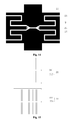
- each of the driving line 22 and the detecting line 24 is an integral conductive layer. Unlike the prior art, in the first embodiment, the driving line 22 or the detecting line 24 is also disposed in a comb-shaped structure. Specifically, referring to FIG 9 , the comb-shaped structure of the driving line 22 includes a bar portion 221 and a comb-shaped portion 222 connected in perpendicular to the bar portion 221. Referring to Figure 10 , the comb-shaped structure of the detecting line 24 includes a bar portion 241 and a comb-shaped portion 242 connected in perpendicular to the bar portion 241.
- the detecting line 24 is specifically disposed as follows.
- the comb-shaped portion 242 of the detecting line 24 is misaligned with respect to the comb-shaped portion 3212 of the pixel electrode 321; or 2) the comb-shaped portion 242 of the detecting line 24 is misaligned with respect to the comb-shaped portion 3222 of the common electrode 322; or 3) the comb-shaped portion 242 of the detecting line 24 is misaligned with respect to both the comb-shaped portion 3212 of the pixel electrode 321 and the comb-shaped portion 3222 of the common electrode 322.
- the driving line 22 is specifically disposed as follows.
- the comb-shaped portion 222 of the driving line 22 is misaligned with respect to the comb-shaped portion 321 of the pixel electrode 321; or 2) the comb-shaped portion 222 of the driving line 22 is misaligned with respect to the comb-shaped portion 3222 of the common electrode 322; or 3) the comb-shaped portion 222 of the driving line 22 is misaligned with respect to both the comb-shaped portion 3212 of the pixel electrode 321 and the comb-shaped portion 3222 of the common electrode 322.
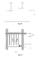
- Figure 11 shows a plan view of a display panel corresponding to one pixel unit when the CF substrate 2 and the TFT substrate 3 are in position and
- Figure 12 shows a sectional view taken along line II-II in Figure 11 .
- the driving line 22 of the CF substrate 2 is misaligned respectively with respect to the comb-shaped portion 3212 of the pixel electrode and the comb-shaped portion 3222 of the common electrode of the TFT substrate 3 which are respectively disposed in two layers.
- the comb-shaped structure of the driving line 22 or the detecting line 24 is at least partially misaligned with respect to the comb-shaped structure of the common electrode 322 and/or the comb-shaped structure of the pixel electrode 321 in the TFT substrate 3 close to the liquid crystal layer 4.
- the common electrode 433322 and the pixel electrode 321 of the TFT substrate 3 are completely overlapped with the driving line 22 and/or the detecting line 24 of the CF substrate 2, thereby reducing the parasitic capacitance.
- the bar portion 3221 of the common electrode 322 is disposed at one end of the comb-shaped portion 3222. It can be understood that the bar portion 3221 is not limited to be disposed at one end of the comb-shaped portion 3222 and may also be disposed in the middle of the comb-shaped portion 3222 as shown in Figure 13 , in order to form the incontinuous gaps.
- the multiple connected comb-shaped portions 3222 are not limited to be connected to one bar portion 3221 and may also be connected to multiple bars portions 3221.
- the multiple connected comb-shaped portions 3212 are not limited to be connected to one bar portion 3211 and may also be connected to multiple bar portions 3211.
- the driving line 22 multiple connected comb-shaped portions 222 are not limited to be connected to one bar portion 221 and may also be connected to multiple bar portions 221.
- the multiple connected comb-shaped portions 242 are not limited to be connected to one bar portion 241 and may also be connected to multiple bar portions 241.
- the bar portion 221 and the comb-shaped portion 222 form the comb-shaped structure of the driving line 22.
- the bar portion 241 and the comb-shaped portion 242 form the comb-shaped structure of the detecting line 24.
- the respective comb-shaped structures are disposed in order to dispose the discontinuous gaps (slits) for the respective integral structures, so as to dispose opening portions for making the electrical field pass through. Therefore, other embodiments are not limited to the comb-shaped structure, as long as the discontinuous gaps can be formed respectively for the driving line 22 and the detecting line 24.
- the common electrode 322 and the pixel electrode 321 are on a same layer and disposed alternately. Sine the common electrode 322 and the pixel electrode 321 are disposed alternately, each of the common electrode 322 and the pixel electrode 321 has a comb-shaped structure. As for the above-mentioned, the common electrode 322 and the pixel electrode 321 are disposed in the same layer, and the touch layer is disposed on the CF substrate 2, the driving line and the detecting line are disposed all over the entire layer in the prior art.
- the driving line 22 or the detecting line 24 is disposed in a comb-shaped structure as well, and the comb-shaped structure is at least partially misaligned with respect to at least one of the comb-shaped structure of the common electrode 322 and the comb-shaped structure of the pixel electrode 321 in the same layer.
- the common electrode 322 and/or the pixel electrode 321 of the TFT substrate 3 are completely overlapped with the driving line 22 or the detecting line 24 of the CF substrate 2, thereby reducing the parasitic capacitance.
- the above-mentioned misaligning includes partially misaligning and completely misaligning.
- the comb-shaped structure of the driving line 22 or the detecting line 24 is at least partially complementary to the comb-shaped structure of the common electrode 322 and/or the comb-shaped structure of the pixel electrode 321 in the same layer.
- the materials of the driving line 22 and the detecting line 24 are transparent, such as indium tin oxide, indium zinc oxide or the combination thereof.
- the materials of the common electrode 322, the gate line 33 and the data line 34 may be metal such as copper and aluminum.
- the materials of the common electrode 322, the gate line 33 and the data line 34 may also be a transparent conductive material, so as to increase the light transmittance.
- the material of the pixel electrode 312 is generally a transparent conductive material.
- the transparent conductive material may also be, for example, indium tin oxide, indium zinc oxide or the combination thereof.
- a liquid crystal alignment layer made of polyimide may also be disposed on the driving line 22 or the detecting line 24.
- the structure of the touch display panel according to the second embodiment is substantially the same as the structure of the touch display panel according to the first embodiment, except that, for the CF substrate 2, the driving line 22 and detecting line 24 are disposed in one touch layer, rather than that the driving line 22 and the detecting line 24 are respectively disposed in two touch layers, as shown in Figure 14 .
- the driving line 22 and the detecting line 24 are isolated with each other via a dielectric layer 23.
- the driving line 22 separates the detecting line 24 into separated portions.
- a first connecting portion 25 is disposed to connect the separated detecting line 24 across the driving line 22.
- the detecting line 24 may also separate the driving line 22 into separated portions.
- a second connecting portion is disposed on the separated portions, the first connecting portion crosses the detecting line 24 to connect the separated driving line 22.
- Figure 15 shows an enlarged view of the region Q in Figure 14 .
- the comb-shaped structure of the driving line 22 includes a bar portion 221 and a comb-shaped portion 222 connected in perpendicular to the bar portion 221.
- the comb-shaped structure of the detecting line 24 includes a bar portion 241 and a comb-shaped portion 242 connected in perpendicular to the bar portion 241.
- the touch layer is specifically disposed as follows.
- One of the comb-shaped portion 222 of the driving line 22 and the comb-shaped portion 242 of the detecting line 24 is misaligned with respect to the comb-shaped portion 3212 of the pixel electrode 321, or, both of the comb-shaped portion 222 of the driving line 22 and the comb-shaped portion 242 of the detecting line 24 are misaligned with respect to the comb-shaped portion 3212 of the pixel electrode 321; or 2) one of the comb-shaped portion 222 of the driving line 22 and the comb-shaped portion 242 of the detecting line 24 is misaligned with respect to the comb-shaped portion 3222 of the common electrode 322, or, both of the comb-shaped portion 222 of the driving line 22 and the comb-shaped portion 242 of the detecting line 24 are misaligned with respect to the comb-shaped portion 3222 of the common electrode 322; or 3) one of the comb-shaped portion 222 of the driving line 22 and the comb-shaped portion 242 of the detecting line 24 is misal
- the comb-shaped structure of the driving line 22 and/or the detecting line 24 is at least partially misaligned with respect to at least one of the comb-shaped structure of the common electrode 322 and the comb-shaped structure of the pixel electrode 321 in the TFT substrate 3 close to the liquid crystal layer 4.
- the above-mentioned misaligning includes partially misaligning and completely misaligning.
- the comb-shaped structure of the driving line 22 and/or the detecting line 24 is at least partially complementary to the comb-shaped structure of the common electrode 322 and/or the comb-shaped structure of the pixel electrode 321 in the TFT substrate 3 close to the liquid crystal layer 4.
- the structure of the touch display panel according to the third embodiment is substantially the same as the structure of the touch display panel according to the first embodiment, the different is that for the TFT substrate 3, the common electrode 322 and the gate line 33 are firstly formed on the glass substrate 31 and then the TFT structure and the pixel electrode 321 are formed. Therefore, the comb-shaped portion 3222 of the common electrode 322 and the comb-shaped portion 3212 of the pixel electrode 321 may not be formed in the same layer, as shown in Figure 16 , one or more insulating layer such as a passivation layer 37 is disposed between the comb-shaped portion 3222 of the common electrode 322 and the comb-shaped portion 3212 of the pixel electrode 321.
- the touch layer is specifically disposed as follows.
- the comb-shaped portion 242 of the detecting line 24 is misaligned with respect to the comb-shaped portion 3212 of the pixel electrode 321.
- the touch layer is specifically disposed as follows.
- the comb-shaped portion 222 of the driving line 22 is misaligned with respect to the comb-shaped portion 3212 of the pixel electrode 321.
- the pixel electrode 321 of the TFT substrate 3 is completely overlapped with the driving line 22 of the CF substrate 2, thereby reducing the parasitic capacitance.
- the touch layer is specifically disposed as follows. Both of the comb-shaped portion 222 of the driving line 22 and the comb-shaped portion 242 of the detecting line 24 are misaligned with respect to the comb-shaped portion 3212 of the pixel electrode 321; or one of the comb-shaped portion 222 of the driving line 22 and the comb-shaped portion 242 of the detecting line 24 is misaligned with respect to the comb-shaped portion 3212 of the pixel electrode 321.
- the pixel electrode 321 of the TFT substrate 3 is completely overlapped with the detecting line 24 and/or the driving line 22 of the CF substrate 2, thereby reducing the parasitic capacitance.
- the comb-shaped structure of the driving line 22 and/or the detecting line 24 is at least partially misaligned with respect to the comb-shaped structure of the pixel electrode 321 in the TFT substrate 3 close to the liquid crystal layer 4.
- the pixel electrode 321 of the TFT substrate 3 is completely overlapped with the driving line 22 and/or the detecting line 24 of the CF substrate 2, thereby reducing the parasitic capacitance.
- the touch layer is specifically disposed as follows:
- the comb-shaped portion 242 of the detecting line 24 is misaligned with respect to the comb-shaped portion 3222 of the common electrode 322.
- the touch layer is specifically disposed as follows:
- the comb-shaped portion 222 of the driving line 22 is misaligned with respect to the comb-shaped portion 3222 of the common electrode 322.
- the touch layer is specifically disposed as follows. Both of the comb-shaped portion 222 of the driving line 22 and the comb-shaped portion 242 of the detecting line 24 are misaligned with respect to the comb-shaped portion 3222 of the common electrode 322; or one of the comb-shaped portion 222 of the driving line 22 and the comb-shaped portion 242 of the detecting line 24 is misaligned with respect to the comb-shaped portion 3222 of the common electrode 322.
- the common electrode 322 of the TFT substrate 3 is completely overlapped with the detecting line 24 and/or the driving line 22 of the CF substrate 2, thereby reducing the parasitic capacitance.
- the comb-shaped structure of the driving line 22 and/or the comb-shaped structure of the detecting line 24 are/is at least partially misaligned with respect to the comb-shaped structure of the common electrode 322 on the TFT substrate 3 close to the liquid crystal layer 4.
- the common electrode 322 of the TFT substrate 3 is completely overlapped with the driving line 22 and/or the detecting line 24 of the CF substrate 2, thereby reducing the parasitic capacitance.
- the comb-shaped structure of the driving line 22 and/or the detecting line 24 are/is at least partially misaligned with respect to the comb-shaped structure of the common electrode 322 or the comb-shaped structure of the pixel electrode 312 on the TFT substrate 3 close to the liquid crystal layer 4.
- the common electrode 322 or the pixel electrode 312 of the TFT substrate 3 is completely overlapped with the driving line 22 and/or the detecting line 24 of the CF substrate 2, thereby reducing the parasitic capacitance.
- the above-mentioned misaligning includes partially misaligning and completely misaligning.
- the comb-shaped structure of the driving line 22 and/or the detecting line 24 is at least partially complementary to the comb-shaped structure of the common electrode 322 or the comb-shaped structure of the pixel electrode 321 on the TFT substrate 3 close to the liquid crystal layer 4.
- the FFS mode has higher light transmittance. This is because, in the FFS mode, the common electrode and the pixel electrode do not have to be disposed alternately, leading to a reduced space therebetween. Therefore, the upper portion of the common electrode or the pixel electrode in the upper electrode layer can also generate a lateral electric field, and the liquid crystal molecules on the corresponding electrode can also be rotated. It is no longer limited to the case in the IPS mode where the lateral electric field only exist between the common electrode and the pixel electrode, each electrode almost has no electric field, and the liquid crystal molecules on each electrode can not be rotated.
- the FFS-LCD touch display panel which operates in the FFS liquid display mode is taken as an example to explain the technical solution of the present invention.
- the FFS-LCD touch display panel includes: a color film (CF) substrate 2 and a thin film transistor (TFT) substrate 3 disposed opposite to each other, and a liquid crystal layer 4 disposed between the CF substrate and the TFT substrate.
- CF color film
- TFT thin film transistor
- the TFT substrate 3 of the FFS-LCD touch display panel is described as follows. Referring to Figure 17 which is plan view of a pixel unit and Figure 18 which a sectional view taken along line III-III in Figure 17 , the TFT substrate 3 includes a glass substrate 31 and a circuit board formed on the glass substrate 31.
- the circuit board includes a data line 34 and a gate line 33 intersecting with each other, a TFT transistor formed at the intersection of the data line 34 and the gate line 33, and a common electrode (line) 322 and a pixel electrode 321, the common electrode (line) 322 is substantially parallel with the gate line 33.
- the gate electrode of the TFT transistor is a portion of the gate line 33
- the source electrode of the TFT transistor is a portion of the data line 34
- the drain electrode of the TFT transistor is connected to the pixel electrode 321 via a via hole (not shown).
- the pixel electrode 321 is an integral conductive layer.
- On the pixel electrode 321, an insulating layer 38 and the common electrode 322 are formed from top to bottom.
- the common electrode 322 has a bar portion 3221 substantially disposed in parallel with the common electrode line and a comb-shaped portion 3222 disposed substantially in perpendicular to the common electrode line.
- the comb-shaped portion 3222 and the pixel electrode 321 are used for providing a voltage to rotate the liquid crystal molecules.
- the bar portion 3221 and the comb-shaped portion 3222 form the comb-shaped structure of the common electrode 322, in order to dispose incontinuous gaps (slits) for the integral structure, so as to dispose an opening portion for making the electrical field pass through. Therefore, other embodiments are not limited to the comb-shaped structure, as long as the discontinuous gaps can be formed for the common electrode 322.
- a protective film 35 may be disposed on the comb-shaped portion 3222 of the common electrode 322, and the material of the protective film 35 may be silicon nitride. More preferably, a liquid crystal alignment layer 36 may further be dispose on the protective film 35, and the material of the liquid crystal alignment layer 36 may be polyimide.
- the glass substrate 31 may also be made of a transparent material such as quartz or flexible plastic as required.
- the touch layer may include a first touch layer and a second touch layer.
- the driving line 22 is formed in the first touch layer
- the detecting line 24 is formed in the second touch layer.
- a dielectric layer 23 is disposed between the two touch layers.
- the driving line 22 and the detecting line 24 may also be disposed in one touch layer.
- the driving line 22 and the detecting line 24 are disposed perpendicularly to each other, so that a touch control signal is detected when a touching body makes a touch at the intersection of the driving line 22 and the detecting line 24.
- the driving line 22 and the detecting line 24 respectively formed in two touch layers may be disposed in the following two ways. 1) The second touch layer disposed with the detecting line 24 is closer to the liquid crystal layer 4 and 2) the first touch layer disposed with the driving line 22 may be closer to the liquid crystal layer 4.
- one unit defined by one driving line 22 and one detecting line 24 may correspond to one pixel unit of the TFT substrate 3 or correspond to multiple pixel units.
- each of the driving line 22 and the detecting line 24 is an integral conductive layer. Unlike the prior art, in the fourth embodiment, the driving line 22 or the detecting line 24 is also disposed in a comb-shaped structure. Specifically, referring again to FIG 9 , the comb-shaped structure of the driving line 22 includes a bar portion 221 and a comb-shaped portion 222 connected in perpendicular to the bar portion 221. Referring to Figure 10 , the comb-shaped structure of the detecting line 24 includes a bar portion 241 and a comb-shaped portion 242 connected in perpendicular to the bar portion 241.
- the touch layer is specifically disposed as follows.
- the comb-shaped portion 242 of the detecting line 24 is misaligned with respect to the comb-shaped portion 3222 of the common electrode 322.
- the touch layer is specifically disposed as follows.
- the comb-shaped portion 222 of the driving line 22 is misaligned with respect to the comb-shaped portion 3222 of the common electrode 322.
- Figure 20 shows a plan view of a display panel corresponding to one pixel unit when the CF substrate 2 and the TFT substrate 3 are in position and
- Figure 21 shows a sectional view taken along line IV-IV in Figure 20 .
- the driving line 22 of the CF substrate 2 is misaligned respectively with respect to the comb-shaped portion 3212 of the pixel electrode and the comb-shaped portion 3222 of the common electrode of the TFT substrate 3, the pixel electrode and the common electrode are respectively disposed in two layers.
- the comb-shaped structure of the driving line 22 or the detecting line 24 is at least partially misaligned with respect to the comb-shaped structure of the common electrode 322 on the TFT substrate 3 close to the liquid crystal layer 4.
- the common electrode 322 of the TFT substrate 3 is completely overlapped with the driving line 22 or the detecting line 24 of the CF substrate 2, thereby reducing the parasitic capacitance.
- the multiple connected comb-shaped portions 3222 are not limited to be connected to one bar portion 3221 and may also be connected to multiple bars portions 3221.
- the multiple connected comb-shaped portions 222 are not limited to be connected to one bar portion 221 and may also be connected to multiple bar portions 221.
- the multiple connected comb-shaped portions 242 are not limited to be connected to one bar portion 241 and may also be connected to multiple bar portions 241.
- both the detecting line 24 and the driving line 22 are not limited to be disposed in the comb-shaped structure, as long as the discontinuous gaps can be formed respectively for the driving line 22 and the detecting line 24.
- the driving line 22 and the detecting line 24 are separated by a dielectric layer 23.
- the driving line 22 and the detecting line 24 are separated with each other in the following two ways. 1)
- the driving line 22 separates the detecting line 24 into separated portions, a first connecting portion 25 is disposed on the separated portions, the first connecting portion 25 crosses the driving line 22 to connect the separated detecting line 24; 2) the detecting line 24 may also separate the driving line 22 into separated portions, a second connecting portion is disposed on the separated portions, the second connecting portion 25 crosses the detecting line 24 to connect the separated driving line 22.
- each of the driving line 22 and the detecting line 24 is an integral conductive layer. Unlike the prior art, in the fourth embodiment, the driving line 22 or the detecting line 24 is also disposed in a comb-shaped structure. Specifically, referring to FIG 9 , the comb-shaped structure of the driving line 22 includes a bar portion 221 and a comb-shaped portion 222 connected in perpendicular to the bar portion 221. Referring to Figure 10 , the comb-shaped structure of the detecting line 24 includes a bar portion 241 and a comb-shaped portion 242 connected in perpendicular to the bar portion 241.
- the touch layer is specifically disposed as follows.
- One of the comb-shaped portion 222 of the driving line 22 and the comb-shaped portion 242 of the detecting line 24 is misaligned with respect to the comb-shaped portion 3222 of the common electrode 322; or both of the comb-shaped portion 222 of the driving line 22 and the comb-shaped portion 242 of the detecting line 24 are misaligned with respect to the comb-shaped portion 3222 of the common electrode 322.
- the comb-shaped structure of the driving line 22 or/and the detecting line 24 is at least partially misaligned with respect to the comb-shaped structure of the common electrode 322 on the TFT substrate 3 close to the liquid crystal layer 4.
- the common electrode 322 of the TFT substrate 3 is completely overlapped with the driving line 22 and/or the detecting line 24 of the CF substrate 2, thereby reducing the parasitic capacitance.
- the above-mentioned misaligning includes partially misaligning and completely misaligning.
- the comb-shaped structure of the driving line 22 and/or the detecting line 24 is at least partially complementary to the comb-shaped structure of the common electrode 322 on the TFT substrate 3 close to the liquid crystal layer 4.
- a liquid crystal alignment layer made of polyimide may also be disposed on the driving line 22 or the detecting line 24.
- the structure of FFS-LCD touch display panel of the fifth embodiment is substantially the same as the structure of the touch display panel of the fourth embodiment, the difference is that for the TFT substrate 3, the common electrode 322 and the gate electrode are disposed in the same layer and are substantially parallel with each other, and the common electrode 322 is an integral conductive layer.
- the pixel electrode 321 is connected to the drain electrode via a hole.
- the pixel electrode 321 includes a bar portion 3211 and a comb-shaped portion 3212 connected in perpendicular to the bar portion 3211.
- the comb-shaped portion 3212 and the common electrode 322 are used for providing a voltage to rotate the liquid crystal molecules.
- the bar portion 3211 and the comb-shaped portion 3212 form the comb-shaped structure of the pixel electrode 321, so as to dispose an opening portion for making the electrical field pass through. Therefore, for other embodiments, the pixel electrode 321 is not limited to the comb-shaped structure, as long as the discontinuous gaps can be formed for the pixel electrode 321.
- the comb-shaped structure of the pixel electrode 321 is formed on the surface of the TFT substrate, the surface is close to the liquid crystal layer 4.
- a protective film may be disposed over the comb-shaped portion 3212 of the pixel electrode 321, and the material of the protective film may be silicon nitride. More preferably, a liquid crystal alignment layer made of polyimide may further be disposed on the protective film.
- the CF substrate 2 is described as follow. Similar to the fourth embodiment, the touch layer may be disposed in the following two ways. 1) The touch layer may include a first touch layer and a second touch layer; a driving line 22 is formed in the first touch layer; a detecting line 24 is formed in the second touch layer; and a dielectric layer 23 is disposed between the two touch layers. 2) The driving line 22 and the detecting line 24 are formed in one touch layer.
- the driving line 22 and the detecting line 24 are disposed perpendicularly to each other, so that a touch control signal may be detected when a touching body makes a touch at the intersection of the driving line 22 and the detecting line 24.
- the driving line 22 and the detecting line 24 respectively formed in two touch layers may be disposed in the following two ways. 1) The second touch layer disposed with the detecting line 24 is closer to the liquid crystal layer 4 and 2) the first touch layer disposed with the driving line 22 may be closer to the liquid crystal layer 4.
- one unit defined by one driving line 22 and one detecting line 24 may correspond to one pixel unit of the TFT substrate 3 or correspond to multiple pixel units.
- each of the driving line 22 and the detecting line 24 is an integral conductive layer. Unlike the prior art, in the fifth embodiment, the driving line 22 or the detecting line 24 is also disposed in a comb-shaped structure. Specifically, referring to FIG 9 , the comb-shaped structure of the driving line 22 includes a bar portion 221 and a comb-shaped portion 222 connected in perpendicular to the bar portion 221. Referring to Figure 10 , the comb-shaped structure of the detecting line 24 includes a bar portion 241 and a comb-shaped portion 242 connected in perpendicular to the bar portion 241.
- the touch layer is specifically disposed as follows.
- the comb-shaped portion 242 of the detecting line 24 is misaligned with respect to the comb-shaped portion 3212 of the pixel electrode 321.
- the touch layer is specifically disposed as follows.
- the comb-shaped portion 222 of the driving line 22 is misaligned with respect to the comb-shaped portion 3212 of the pixel electrode 321.
- the pixel electrode 321 of the TFT substrate 3 is completely overlapped with the driving line 22 of the CF substrate 2, thereby reducing the parasitic capacitance.
- the comb-shaped structure of the driving line 22 or the detecting line 24 is at least partially misaligned with respect to the comb-shaped structure of the pixel electrode 321 on the TFT substrate 3 close to the liquid crystal layer 4.
- the pixel electrode 321 of the TFT substrate 3 is completely overlapped with the driving line 22 and/or the detecting line 24 of the CF substrate 2, thereby reducing the parasitic capacitance.
- the multiple connected comb-shaped portions 3212 are not limited to be connected to one bar portion 3211 and may also be connected to multiple bars portions 3211.
- the multiple connected comb-shaped portions 222 are not limited to be connected to one bar portion 221 and may also be connected to multiple bar portions 221.
- the multiple connected comb-shaped portions 242 are not limited to be connected to one bar portion 241 and may also be connected to multiple bar portions 241.
- both the detecting line 24 and the driving line 22 are not limited to be disposed in the comb-shaped structure, as long as the discontinuous gaps can be formed respectively for the driving line 22 and the detecting line 24.
- the driving line 22 and the detecting line 24 are separated by a dielectric layer 23.
- the driving line 22 and the detecting line 24 are separated with each other in the following two ways. 1)
- the driving line 22 separates the detecting line 24 into separated portions, a first connecting portion 25 is disposed on the separated portions, the first connecting portion 25 crosses the driving line 22 to connect the separated detecting line 24; 2) the detecting line 24 may also separate the driving line 22 into separated portions, a second connecting portion is disposed on the separated portions, the second connecting portion crosses the detecting line 24 to connect the separated driving line 22.
- each of the driving line 22 and the detecting line 24 is an integral conductive layer. Unlike the prior art, in the fifth embodiment, the driving line 22 or the detecting line 24 is also disposed in a comb-shaped structure.
- the comb-shaped structure of the driving line 22 includes a bar portion 221 and a comb-shaped portion 222 connected in perpendicular to the bar portion 221.
- the comb-shaped structure of the detecting line 24 includes a bar portion 241 and a comb-shaped portion 242 connected in perpendicular to the bar portion 241.
- the touch layer is specifically disposed as follows.
- One of the comb-shaped portion 222 of the driving line 22 and the comb-shaped portion 242 of the detecting line 24 is misaligned with respect to the comb-shaped portion 3212 of the pixel electrode 321, or both of the comb-shaped portion 222 of the driving line 22 and the comb-shaped portion 242 of the detecting line 24 are misaligned with respect to the comb-shaped portion 3212 of the pixel electrode 321.
- the pixel electrode 321 of the TFT substrate 3 is completely overlapped with the detecting line 24 and/or the driving line 22 of the CF substrate 2, thereby reducing the parasitic capacitance.
- the comb-shaped structure of the driving line 22 or/and the detecting line 24 are at least partially misaligned with respect to the comb-shaped structure of the pixel electrode 321 on the TFT substrate 3 close to the liquid crystal layer 4.
- the pixel electrode 321 of the TFT substrate 3 is completely overlapped with the driving line 22 and/or the detecting line 24 of the CF substrate 2, thereby reducing the parasitic capacitance.
- the above-mentioned misaligning includes partially misaligning and completely misaligning.
- the comb-shaped structure of the driving line 22 and/or the detecting line 24 is at least partially complementary to the comb-shaped structure of the common electrode 322 on the TFT substrate 3 close to the liquid crystal layer 4.
- a liquid crystal alignment layer made of polyimide may also be disposed on the driving line 22 and/or the detecting line 24.
Landscapes
- Engineering & Computer Science (AREA)
- General Engineering & Computer Science (AREA)
- Theoretical Computer Science (AREA)
- Physics & Mathematics (AREA)
- General Physics & Mathematics (AREA)
- Human Computer Interaction (AREA)
- Quality & Reliability (AREA)
- Nonlinear Science (AREA)
- Liquid Crystal (AREA)
- Mathematical Physics (AREA)
- Chemical & Material Sciences (AREA)
- Crystallography & Structural Chemistry (AREA)
- Optics & Photonics (AREA)
Applications Claiming Priority (2)
| Application Number | Priority Date | Filing Date | Title |
|---|---|---|---|
| CN201210253996.8A CN103294246B (zh) | 2012-07-20 | 2012-07-20 | 触摸显示面板 |
| PCT/CN2012/085946 WO2014012319A1 (fr) | 2012-07-20 | 2012-12-05 | Panneau d'affichage tactile |
Publications (3)
| Publication Number | Publication Date |
|---|---|
| EP2706442A1 true EP2706442A1 (fr) | 2014-03-12 |
| EP2706442A4 EP2706442A4 (fr) | 2015-07-08 |
| EP2706442B1 EP2706442B1 (fr) | 2022-04-27 |
Family
ID=49095254
Family Applications (1)
| Application Number | Title | Priority Date | Filing Date |
|---|---|---|---|
| EP12868921.3A Not-in-force EP2706442B1 (fr) | 2012-07-20 | 2012-12-05 | Panneau d'affichage tactile |
Country Status (5)
| Country | Link |
|---|---|
| US (1) | US9588368B2 (fr) |
| EP (1) | EP2706442B1 (fr) |
| KR (1) | KR101534425B1 (fr) |
| CN (1) | CN103294246B (fr) |
| WO (1) | WO2014012319A1 (fr) |
Cited By (2)
| Publication number | Priority date | Publication date | Assignee | Title |
|---|---|---|---|---|
| EP3614242A4 (fr) * | 2017-11-30 | 2020-08-12 | Kunshan Go-Visionox Opto-Electronics Co., Ltd. | Panneau tactile et dispositif d'affichage tactile |
| EP3816777A1 (fr) * | 2019-10-30 | 2021-05-05 | LG Display Co., Ltd. | Afficheur tactile et panneau tactile |
Families Citing this family (20)
| Publication number | Priority date | Publication date | Assignee | Title |
|---|---|---|---|---|
| US9645431B2 (en) * | 2008-03-19 | 2017-05-09 | Egalax_Empia Technology Inc. | Touch display and method for driving a plurality of touch driving electrodes of touch display |
| KR102128394B1 (ko) * | 2013-09-11 | 2020-07-01 | 삼성디스플레이 주식회사 | 터치 감지 표시 장치 |
| CN103529607B (zh) | 2013-10-29 | 2017-05-31 | 京东方科技集团股份有限公司 | 一种液晶显示面板、显示装置及其驱动方法 |
| CN103955309B (zh) * | 2014-04-14 | 2017-08-25 | 京东方科技集团股份有限公司 | 显示面板及其驱动方法、显示装置 |
| CN103995617B (zh) * | 2014-05-30 | 2018-09-07 | 京东方科技集团股份有限公司 | 内嵌式触控显示面板、其操作方法及显示装置 |
| US20160034063A1 (en) * | 2014-07-29 | 2016-02-04 | Hannstar Display (Nanjing) Corporation | Anti-interference touch display panel |
| KR102230808B1 (ko) * | 2014-10-13 | 2021-03-24 | 삼성디스플레이 주식회사 | 터치 스크린 패널 |
| KR102316583B1 (ko) * | 2014-10-13 | 2021-10-26 | 삼성디스플레이 주식회사 | 터치 스크린 패널 |
| CN104503648B (zh) * | 2015-01-09 | 2017-06-09 | 京东方科技集团股份有限公司 | 一种内嵌式触摸屏及显示装置 |
| CN105094422B (zh) * | 2015-06-23 | 2018-09-11 | 京东方科技集团股份有限公司 | 一种触控显示面板、其制备方法、驱动方法及显示装置 |
| CN105093736A (zh) * | 2015-07-14 | 2015-11-25 | 京东方科技集团股份有限公司 | Ips阵列基板及其制作方法、显示器件 |
| CN105826328B (zh) * | 2016-05-03 | 2019-03-05 | 京东方科技集团股份有限公司 | 阵列基板及其制造方法、显示装置 |
| WO2017195339A1 (fr) * | 2016-05-13 | 2017-11-16 | 凸版印刷株式会社 | Dispositif d'affichage |
| TWI596527B (zh) * | 2016-12-14 | 2017-08-21 | 友達光電股份有限公司 | 觸控顯示裝置 |
| CN109557728B (zh) * | 2017-09-25 | 2021-12-10 | 京东方科技集团股份有限公司 | 像素结构及其制作方法、阵列基板和触控显示装置 |
| TWI654548B (zh) * | 2017-10-27 | 2019-03-21 | 友達光電股份有限公司 | 觸控裝置 |
| CN108803945B (zh) * | 2018-09-05 | 2024-04-12 | 京东方科技集团股份有限公司 | 一种触摸屏及显示设备 |
| CN111540713B (zh) * | 2020-05-09 | 2022-07-26 | 青岛三顺智能电器有限公司 | 一种触摸显示面板及其制造方法 |
| CN114698267B (zh) * | 2021-08-09 | 2024-06-04 | 上海航天电子通讯设备研究所 | Lcp多层柔性电路板曲面成型方法 |
| KR20250035693A (ko) * | 2023-09-05 | 2025-03-13 | 삼성디스플레이 주식회사 | 터치 패널 및 이를 포함하는 표시 장치 |
Family Cites Families (12)
| Publication number | Priority date | Publication date | Assignee | Title |
|---|---|---|---|---|
| JP3444540B2 (ja) * | 2000-10-17 | 2003-09-08 | 松下電器産業株式会社 | アクティブマトリックス型液晶表示装置 |
| JP3774858B2 (ja) * | 2001-04-07 | 2006-05-17 | 大林精工株式会社 | 液晶表示装置とその駆動方法 |
| CN104965621B (zh) * | 2006-06-09 | 2018-06-12 | 苹果公司 | 触摸屏液晶显示器及其操作方法 |
| JP4916852B2 (ja) * | 2006-11-29 | 2012-04-18 | 株式会社 日立ディスプレイズ | タッチパネル付き液晶表示装置 |
| CN101556390B (zh) * | 2008-04-09 | 2012-07-18 | 北京京东方光电科技有限公司 | 用于三维显示装置的开关面板和液晶显示系统 |
| JP2009265512A (ja) * | 2008-04-28 | 2009-11-12 | Sony Corp | 液晶表示装置 |
| JP5206250B2 (ja) * | 2008-05-02 | 2013-06-12 | セイコーエプソン株式会社 | 表示装置および電子機器 |
| TWI497157B (zh) * | 2009-06-19 | 2015-08-21 | Tpk Touch Solutions Inc | 具觸控功能的平面轉換式液晶顯示器 |
| CN101930132A (zh) * | 2009-06-22 | 2010-12-29 | 上海天马微电子有限公司 | 集成触摸屏及集成触摸屏的检测方法 |
| KR20120017587A (ko) * | 2010-08-19 | 2012-02-29 | 삼성모바일디스플레이주식회사 | 터치스크린패널 일체형 액정표시장치 |
| TW201227454A (en) * | 2010-12-31 | 2012-07-01 | Hong-Da Liu | An active array having the touchable sensing matrix unit and a display having the active array |
| JP5789113B2 (ja) * | 2011-03-31 | 2015-10-07 | 株式会社Joled | 表示装置および電子機器 |
-
2012
- 2012-07-20 CN CN201210253996.8A patent/CN103294246B/zh not_active Expired - Fee Related
- 2012-12-05 WO PCT/CN2012/085946 patent/WO2014012319A1/fr not_active Ceased
- 2012-12-05 KR KR1020137022555A patent/KR101534425B1/ko not_active Expired - Fee Related
- 2012-12-05 EP EP12868921.3A patent/EP2706442B1/fr not_active Not-in-force
-
2013
- 2013-08-30 US US14/014,948 patent/US9588368B2/en not_active Expired - Fee Related
Cited By (3)
| Publication number | Priority date | Publication date | Assignee | Title |
|---|---|---|---|---|
| EP3614242A4 (fr) * | 2017-11-30 | 2020-08-12 | Kunshan Go-Visionox Opto-Electronics Co., Ltd. | Panneau tactile et dispositif d'affichage tactile |
| EP3816777A1 (fr) * | 2019-10-30 | 2021-05-05 | LG Display Co., Ltd. | Afficheur tactile et panneau tactile |
| US11175778B2 (en) | 2019-10-30 | 2021-11-16 | Lg Display Co., Ltd. | Touch display device and display panel |
Also Published As
| Publication number | Publication date |
|---|---|
| KR101534425B1 (ko) | 2015-07-06 |
| CN103294246B (zh) | 2016-03-16 |
| WO2014012319A1 (fr) | 2014-01-23 |
| EP2706442B1 (fr) | 2022-04-27 |
| KR20140048083A (ko) | 2014-04-23 |
| US9588368B2 (en) | 2017-03-07 |
| US20140022210A1 (en) | 2014-01-23 |
| CN103294246A (zh) | 2013-09-11 |
| EP2706442A4 (fr) | 2015-07-08 |
Similar Documents
| Publication | Publication Date | Title |
|---|---|---|
| EP2706442B1 (fr) | Panneau d'affichage tactile | |
| US8300027B2 (en) | Vibration touch sensor, method for vibration touch sensing and vibration touch screen display panel | |
| US8525797B2 (en) | Touch screen display with electric field shielding layer | |
| US8937690B2 (en) | Liquid crystal display device having touch panel | |
| CN102402356B (zh) | 具有触摸检测功能的显示装置以及电子单元 | |
| KR101428568B1 (ko) | 터치스크린을 포함하는 표시장치 및 그 구동 방법 | |
| EP2472362B1 (fr) | Panneau d'affichage tactile, panneau tactile, dispositif tactile et circuit tactile | |
| CN201107503Y (zh) | 具有电场屏蔽层的触控显示面板 | |
| EP2527912B1 (fr) | Panneau d'affichage à cristaux liquides et procédé de commande correspondant | |
| US20130265282A1 (en) | Touch panel and display device with touch panel | |
| CN103186297B (zh) | 一种电容式触摸液晶显示面板和液晶显示装置 | |
| EP2804043A1 (fr) | Substrat matriciel, panneau d'affichage à cristaux liquides tactile et son procédé de fabrication | |
| US9715137B2 (en) | Liquid crystal display device using in-cell touch mode and method for manufacturing the same | |
| TW201350974A (zh) | 增加觸控位置準確度之內嵌式觸控顯示面板系統 | |
| CN106445261A (zh) | 触控显示设备 | |
| US20160377898A1 (en) | Ips in-cell touch display panel and manufacturing method thereof | |
| KR101673206B1 (ko) | 셀프 커패시터 방식 인셀 터치 액정표시장치 | |
| WO2017020357A1 (fr) | Structure de panneau d'affichage tactile intégré de type va | |
| CN107505793B (zh) | 阵列基板和显示装置 | |
| KR20100074820A (ko) | 진동 터치 스크린 패널과 그 제조 방법 | |
| CN104145239A (zh) | 输入装置 | |
| CN106802503B (zh) | 液晶显示面板 | |
| US20150324083A1 (en) | Touch-screen Display Device | |
| KR20140098386A (ko) | 터치 스크린 일체형 디스플레이 장치와 이의 구동방법 | |
| KR20090125655A (ko) | 터치 패널 일체형 평판 디스플레이 장치 |
Legal Events
| Date | Code | Title | Description |
|---|---|---|---|
| PUAI | Public reference made under article 153(3) epc to a published international application that has entered the european phase |
Free format text: ORIGINAL CODE: 0009012 |
|
| 17P | Request for examination filed |
Effective date: 20130826 |
|
| AK | Designated contracting states |
Kind code of ref document: A1 Designated state(s): AL AT BE BG CH CY CZ DE DK EE ES FI FR GB GR HR HU IE IS IT LI LT LU LV MC MK MT NL NO PL PT RO RS SE SI SK SM TR |
|
| RA4 | Supplementary search report drawn up and despatched (corrected) |
Effective date: 20150608 |
|
| RIC1 | Information provided on ipc code assigned before grant |
Ipc: G06F 3/041 20060101AFI20150601BHEP Ipc: G06F 3/044 20060101ALI20150601BHEP |
|
| DAX | Request for extension of the european patent (deleted) | ||
| STAA | Information on the status of an ep patent application or granted ep patent |
Free format text: STATUS: EXAMINATION IS IN PROGRESS |
|
| 17Q | First examination report despatched |
Effective date: 20190710 |
|
| GRAP | Despatch of communication of intention to grant a patent |
Free format text: ORIGINAL CODE: EPIDOSNIGR1 |
|
| STAA | Information on the status of an ep patent application or granted ep patent |
Free format text: STATUS: GRANT OF PATENT IS INTENDED |
|
| INTG | Intention to grant announced |
Effective date: 20211201 |
|
| GRAS | Grant fee paid |
Free format text: ORIGINAL CODE: EPIDOSNIGR3 |
|
| GRAA | (expected) grant |
Free format text: ORIGINAL CODE: 0009210 |
|
| STAA | Information on the status of an ep patent application or granted ep patent |
Free format text: STATUS: THE PATENT HAS BEEN GRANTED |
|
| AK | Designated contracting states |
Kind code of ref document: B1 Designated state(s): AL AT BE BG CH CY CZ DE DK EE ES FI FR GB GR HR HU IE IS IT LI LT LU LV MC MK MT NL NO PL PT RO RS SE SI SK SM TR |
|
| REG | Reference to a national code |
Ref country code: GB Ref legal event code: FG4D |
|
| REG | Reference to a national code |
Ref country code: CH Ref legal event code: EP |
|
| REG | Reference to a national code |
Ref country code: AT Ref legal event code: REF Ref document number: 1487463 Country of ref document: AT Kind code of ref document: T Effective date: 20220515 |
|
| REG | Reference to a national code |
Ref country code: DE Ref legal event code: R096 Ref document number: 602012078114 Country of ref document: DE |
|
| REG | Reference to a national code |
Ref country code: IE Ref legal event code: FG4D |
|
| REG | Reference to a national code |
Ref country code: LT Ref legal event code: MG9D |
|
| REG | Reference to a national code |
Ref country code: NL Ref legal event code: MP Effective date: 20220427 |
|
| REG | Reference to a national code |
Ref country code: AT Ref legal event code: MK05 Ref document number: 1487463 Country of ref document: AT Kind code of ref document: T Effective date: 20220427 |
|
| PG25 | Lapsed in a contracting state [announced via postgrant information from national office to epo] |
Ref country code: NL Free format text: LAPSE BECAUSE OF FAILURE TO SUBMIT A TRANSLATION OF THE DESCRIPTION OR TO PAY THE FEE WITHIN THE PRESCRIBED TIME-LIMIT Effective date: 20220427 |
|
| PG25 | Lapsed in a contracting state [announced via postgrant information from national office to epo] |
Ref country code: SE Free format text: LAPSE BECAUSE OF FAILURE TO SUBMIT A TRANSLATION OF THE DESCRIPTION OR TO PAY THE FEE WITHIN THE PRESCRIBED TIME-LIMIT Effective date: 20220427 Ref country code: PT Free format text: LAPSE BECAUSE OF FAILURE TO SUBMIT A TRANSLATION OF THE DESCRIPTION OR TO PAY THE FEE WITHIN THE PRESCRIBED TIME-LIMIT Effective date: 20220829 Ref country code: NO Free format text: LAPSE BECAUSE OF FAILURE TO SUBMIT A TRANSLATION OF THE DESCRIPTION OR TO PAY THE FEE WITHIN THE PRESCRIBED TIME-LIMIT Effective date: 20220727 Ref country code: LT Free format text: LAPSE BECAUSE OF FAILURE TO SUBMIT A TRANSLATION OF THE DESCRIPTION OR TO PAY THE FEE WITHIN THE PRESCRIBED TIME-LIMIT Effective date: 20220427 Ref country code: HR Free format text: LAPSE BECAUSE OF FAILURE TO SUBMIT A TRANSLATION OF THE DESCRIPTION OR TO PAY THE FEE WITHIN THE PRESCRIBED TIME-LIMIT Effective date: 20220427 Ref country code: GR Free format text: LAPSE BECAUSE OF FAILURE TO SUBMIT A TRANSLATION OF THE DESCRIPTION OR TO PAY THE FEE WITHIN THE PRESCRIBED TIME-LIMIT Effective date: 20220728 Ref country code: FI Free format text: LAPSE BECAUSE OF FAILURE TO SUBMIT A TRANSLATION OF THE DESCRIPTION OR TO PAY THE FEE WITHIN THE PRESCRIBED TIME-LIMIT Effective date: 20220427 Ref country code: ES Free format text: LAPSE BECAUSE OF FAILURE TO SUBMIT A TRANSLATION OF THE DESCRIPTION OR TO PAY THE FEE WITHIN THE PRESCRIBED TIME-LIMIT Effective date: 20220427 Ref country code: BG Free format text: LAPSE BECAUSE OF FAILURE TO SUBMIT A TRANSLATION OF THE DESCRIPTION OR TO PAY THE FEE WITHIN THE PRESCRIBED TIME-LIMIT Effective date: 20220727 Ref country code: AT Free format text: LAPSE BECAUSE OF FAILURE TO SUBMIT A TRANSLATION OF THE DESCRIPTION OR TO PAY THE FEE WITHIN THE PRESCRIBED TIME-LIMIT Effective date: 20220427 |
|
| PG25 | Lapsed in a contracting state [announced via postgrant information from national office to epo] |
Ref country code: RS Free format text: LAPSE BECAUSE OF FAILURE TO SUBMIT A TRANSLATION OF THE DESCRIPTION OR TO PAY THE FEE WITHIN THE PRESCRIBED TIME-LIMIT Effective date: 20220427 Ref country code: PL Free format text: LAPSE BECAUSE OF FAILURE TO SUBMIT A TRANSLATION OF THE DESCRIPTION OR TO PAY THE FEE WITHIN THE PRESCRIBED TIME-LIMIT Effective date: 20220427 Ref country code: LV Free format text: LAPSE BECAUSE OF FAILURE TO SUBMIT A TRANSLATION OF THE DESCRIPTION OR TO PAY THE FEE WITHIN THE PRESCRIBED TIME-LIMIT Effective date: 20220427 Ref country code: IS Free format text: LAPSE BECAUSE OF FAILURE TO SUBMIT A TRANSLATION OF THE DESCRIPTION OR TO PAY THE FEE WITHIN THE PRESCRIBED TIME-LIMIT Effective date: 20220827 |
|
| REG | Reference to a national code |
Ref country code: DE Ref legal event code: R097 Ref document number: 602012078114 Country of ref document: DE |
|
| PG25 | Lapsed in a contracting state [announced via postgrant information from national office to epo] |
Ref country code: SM Free format text: LAPSE BECAUSE OF FAILURE TO SUBMIT A TRANSLATION OF THE DESCRIPTION OR TO PAY THE FEE WITHIN THE PRESCRIBED TIME-LIMIT Effective date: 20220427 Ref country code: SK Free format text: LAPSE BECAUSE OF FAILURE TO SUBMIT A TRANSLATION OF THE DESCRIPTION OR TO PAY THE FEE WITHIN THE PRESCRIBED TIME-LIMIT Effective date: 20220427 Ref country code: RO Free format text: LAPSE BECAUSE OF FAILURE TO SUBMIT A TRANSLATION OF THE DESCRIPTION OR TO PAY THE FEE WITHIN THE PRESCRIBED TIME-LIMIT Effective date: 20220427 Ref country code: EE Free format text: LAPSE BECAUSE OF FAILURE TO SUBMIT A TRANSLATION OF THE DESCRIPTION OR TO PAY THE FEE WITHIN THE PRESCRIBED TIME-LIMIT Effective date: 20220427 Ref country code: DK Free format text: LAPSE BECAUSE OF FAILURE TO SUBMIT A TRANSLATION OF THE DESCRIPTION OR TO PAY THE FEE WITHIN THE PRESCRIBED TIME-LIMIT Effective date: 20220427 Ref country code: CZ Free format text: LAPSE BECAUSE OF FAILURE TO SUBMIT A TRANSLATION OF THE DESCRIPTION OR TO PAY THE FEE WITHIN THE PRESCRIBED TIME-LIMIT Effective date: 20220427 |
|
| PGFP | Annual fee paid to national office [announced via postgrant information from national office to epo] |
Ref country code: DE Payment date: 20221213 Year of fee payment: 11 |
|
| PLBE | No opposition filed within time limit |
Free format text: ORIGINAL CODE: 0009261 |
|
| STAA | Information on the status of an ep patent application or granted ep patent |
Free format text: STATUS: NO OPPOSITION FILED WITHIN TIME LIMIT |
|
| PG25 | Lapsed in a contracting state [announced via postgrant information from national office to epo] |
Ref country code: AL Free format text: LAPSE BECAUSE OF FAILURE TO SUBMIT A TRANSLATION OF THE DESCRIPTION OR TO PAY THE FEE WITHIN THE PRESCRIBED TIME-LIMIT Effective date: 20220427 |
|
| 26N | No opposition filed |
Effective date: 20230130 |
|
| PG25 | Lapsed in a contracting state [announced via postgrant information from national office to epo] |
Ref country code: SI Free format text: LAPSE BECAUSE OF FAILURE TO SUBMIT A TRANSLATION OF THE DESCRIPTION OR TO PAY THE FEE WITHIN THE PRESCRIBED TIME-LIMIT Effective date: 20220427 |
|
| REG | Reference to a national code |
Ref country code: CH Ref legal event code: PL |
|
| GBPC | Gb: european patent ceased through non-payment of renewal fee |
Effective date: 20221205 |
|
| REG | Reference to a national code |
Ref country code: BE Ref legal event code: MM Effective date: 20221231 |
|
| PG25 | Lapsed in a contracting state [announced via postgrant information from national office to epo] |
Ref country code: LU Free format text: LAPSE BECAUSE OF NON-PAYMENT OF DUE FEES Effective date: 20221205 |
|
| PG25 | Lapsed in a contracting state [announced via postgrant information from national office to epo] |
Ref country code: LI Free format text: LAPSE BECAUSE OF NON-PAYMENT OF DUE FEES Effective date: 20221231 Ref country code: IE Free format text: LAPSE BECAUSE OF NON-PAYMENT OF DUE FEES Effective date: 20221205 Ref country code: GB Free format text: LAPSE BECAUSE OF NON-PAYMENT OF DUE FEES Effective date: 20221205 Ref country code: CH Free format text: LAPSE BECAUSE OF NON-PAYMENT OF DUE FEES Effective date: 20221231 |
|
| PG25 | Lapsed in a contracting state [announced via postgrant information from national office to epo] |
Ref country code: FR Free format text: LAPSE BECAUSE OF NON-PAYMENT OF DUE FEES Effective date: 20221231 Ref country code: BE Free format text: LAPSE BECAUSE OF NON-PAYMENT OF DUE FEES Effective date: 20221231 |
|
| PG25 | Lapsed in a contracting state [announced via postgrant information from national office to epo] |
Ref country code: IT Free format text: LAPSE BECAUSE OF FAILURE TO SUBMIT A TRANSLATION OF THE DESCRIPTION OR TO PAY THE FEE WITHIN THE PRESCRIBED TIME-LIMIT Effective date: 20220427 |
|
| PG25 | Lapsed in a contracting state [announced via postgrant information from national office to epo] |
Ref country code: HU Free format text: LAPSE BECAUSE OF FAILURE TO SUBMIT A TRANSLATION OF THE DESCRIPTION OR TO PAY THE FEE WITHIN THE PRESCRIBED TIME-LIMIT; INVALID AB INITIO Effective date: 20121205 |
|
| PG25 | Lapsed in a contracting state [announced via postgrant information from national office to epo] |
Ref country code: CY Free format text: LAPSE BECAUSE OF FAILURE TO SUBMIT A TRANSLATION OF THE DESCRIPTION OR TO PAY THE FEE WITHIN THE PRESCRIBED TIME-LIMIT Effective date: 20220427 |
|
| PG25 | Lapsed in a contracting state [announced via postgrant information from national office to epo] |
Ref country code: MK Free format text: LAPSE BECAUSE OF FAILURE TO SUBMIT A TRANSLATION OF THE DESCRIPTION OR TO PAY THE FEE WITHIN THE PRESCRIBED TIME-LIMIT Effective date: 20220427 |
|
| PG25 | Lapsed in a contracting state [announced via postgrant information from national office to epo] |
Ref country code: MC Free format text: LAPSE BECAUSE OF FAILURE TO SUBMIT A TRANSLATION OF THE DESCRIPTION OR TO PAY THE FEE WITHIN THE PRESCRIBED TIME-LIMIT Effective date: 20220427 |
|
| PG25 | Lapsed in a contracting state [announced via postgrant information from national office to epo] |
Ref country code: TR Free format text: LAPSE BECAUSE OF FAILURE TO SUBMIT A TRANSLATION OF THE DESCRIPTION OR TO PAY THE FEE WITHIN THE PRESCRIBED TIME-LIMIT Effective date: 20220427 Ref country code: MC Free format text: LAPSE BECAUSE OF FAILURE TO SUBMIT A TRANSLATION OF THE DESCRIPTION OR TO PAY THE FEE WITHIN THE PRESCRIBED TIME-LIMIT Effective date: 20220427 |
|
| REG | Reference to a national code |
Ref country code: DE Ref legal event code: R119 Ref document number: 602012078114 Country of ref document: DE |
|
| PG25 | Lapsed in a contracting state [announced via postgrant information from national office to epo] |
Ref country code: MT Free format text: LAPSE BECAUSE OF FAILURE TO SUBMIT A TRANSLATION OF THE DESCRIPTION OR TO PAY THE FEE WITHIN THE PRESCRIBED TIME-LIMIT Effective date: 20220427 |
|
| PG25 | Lapsed in a contracting state [announced via postgrant information from national office to epo] |
Ref country code: DE Free format text: LAPSE BECAUSE OF NON-PAYMENT OF DUE FEES Effective date: 20240702 |
|
| PG25 | Lapsed in a contracting state [announced via postgrant information from national office to epo] |
Ref country code: DE Free format text: LAPSE BECAUSE OF NON-PAYMENT OF DUE FEES Effective date: 20240702 |
|
| PG25 | Lapsed in a contracting state [announced via postgrant information from national office to epo] |
Ref country code: BG Free format text: LAPSE BECAUSE OF FAILURE TO SUBMIT A TRANSLATION OF THE DESCRIPTION OR TO PAY THE FEE WITHIN THE PRESCRIBED TIME-LIMIT Effective date: 20220427 |
|
| PG25 | Lapsed in a contracting state [announced via postgrant information from national office to epo] |
Ref country code: BG Free format text: LAPSE BECAUSE OF FAILURE TO SUBMIT A TRANSLATION OF THE DESCRIPTION OR TO PAY THE FEE WITHIN THE PRESCRIBED TIME-LIMIT Effective date: 20220427 |