EP2708942B1 - Panneau d'affichage et appareil d'affichage comprenant celui-ci - Google Patents
Panneau d'affichage et appareil d'affichage comprenant celui-ci Download PDFInfo
- Publication number
- EP2708942B1 EP2708942B1 EP13178760.8A EP13178760A EP2708942B1 EP 2708942 B1 EP2708942 B1 EP 2708942B1 EP 13178760 A EP13178760 A EP 13178760A EP 2708942 B1 EP2708942 B1 EP 2708942B1
- Authority
- EP
- European Patent Office
- Prior art keywords
- light
- lines
- display
- signal
- image
- Prior art date
- Legal status (The legal status is an assumption and is not a legal conclusion. Google has not performed a legal analysis and makes no representation as to the accuracy of the status listed.)
- Not-in-force
Links
Images


Classifications
-
- G—PHYSICS
- G09—EDUCATION; CRYPTOGRAPHY; DISPLAY; ADVERTISING; SEALS
- G09G—ARRANGEMENTS OR CIRCUITS FOR CONTROL OF INDICATING DEVICES USING STATIC MEANS TO PRESENT VARIABLE INFORMATION
- G09G5/00—Control arrangements or circuits for visual indicators common to cathode-ray tube indicators and other visual indicators
- G09G5/10—Intensity circuits
-
- G—PHYSICS
- G02—OPTICS
- G02F—OPTICAL DEVICES OR ARRANGEMENTS FOR THE CONTROL OF LIGHT BY MODIFICATION OF THE OPTICAL PROPERTIES OF THE MEDIA OF THE ELEMENTS INVOLVED THEREIN; NON-LINEAR OPTICS; FREQUENCY-CHANGING OF LIGHT; OPTICAL LOGIC ELEMENTS; OPTICAL ANALOGUE/DIGITAL CONVERTERS
- G02F1/00—Devices or arrangements for the control of the intensity, colour, phase, polarisation or direction of light arriving from an independent light source, e.g. switching, gating or modulating; Non-linear optics
- G02F1/01—Devices or arrangements for the control of the intensity, colour, phase, polarisation or direction of light arriving from an independent light source, e.g. switching, gating or modulating; Non-linear optics for the control of the intensity, phase, polarisation or colour
- G02F1/13—Devices or arrangements for the control of the intensity, colour, phase, polarisation or direction of light arriving from an independent light source, e.g. switching, gating or modulating; Non-linear optics for the control of the intensity, phase, polarisation or colour based on liquid crystals, e.g. single liquid crystal display cells
- G02F1/133—Constructional arrangements; Operation of liquid crystal cells; Circuit arrangements
- G02F1/1333—Constructional arrangements; Manufacturing methods
- G02F1/1335—Structural association of cells with optical devices, e.g. polarisers or reflectors
- G02F1/1336—Illuminating devices
- G02F1/133602—Direct backlight
- G02F1/133606—Direct backlight including a specially adapted diffusing, scattering or light controlling members
-
- G—PHYSICS
- G09—EDUCATION; CRYPTOGRAPHY; DISPLAY; ADVERTISING; SEALS
- G09F—DISPLAYING; ADVERTISING; SIGNS; LABELS OR NAME-PLATES; SEALS
- G09F9/00—Indicating arrangements for variable information in which the information is built-up on a support by selection or combination of individual elements
-
- G—PHYSICS
- G02—OPTICS
- G02F—OPTICAL DEVICES OR ARRANGEMENTS FOR THE CONTROL OF LIGHT BY MODIFICATION OF THE OPTICAL PROPERTIES OF THE MEDIA OF THE ELEMENTS INVOLVED THEREIN; NON-LINEAR OPTICS; FREQUENCY-CHANGING OF LIGHT; OPTICAL LOGIC ELEMENTS; OPTICAL ANALOGUE/DIGITAL CONVERTERS
- G02F1/00—Devices or arrangements for the control of the intensity, colour, phase, polarisation or direction of light arriving from an independent light source, e.g. switching, gating or modulating; Non-linear optics
- G02F1/01—Devices or arrangements for the control of the intensity, colour, phase, polarisation or direction of light arriving from an independent light source, e.g. switching, gating or modulating; Non-linear optics for the control of the intensity, phase, polarisation or colour
- G02F1/13—Devices or arrangements for the control of the intensity, colour, phase, polarisation or direction of light arriving from an independent light source, e.g. switching, gating or modulating; Non-linear optics for the control of the intensity, phase, polarisation or colour based on liquid crystals, e.g. single liquid crystal display cells
- G02F1/133—Constructional arrangements; Operation of liquid crystal cells; Circuit arrangements
- G02F1/136—Liquid crystal cells structurally associated with a semi-conducting layer or substrate, e.g. cells forming part of an integrated circuit
- G02F1/1362—Active matrix addressed cells
- G02F1/136286—Wiring, e.g. gate line, drain line
-
- G—PHYSICS
- G09—EDUCATION; CRYPTOGRAPHY; DISPLAY; ADVERTISING; SEALS
- G09G—ARRANGEMENTS OR CIRCUITS FOR CONTROL OF INDICATING DEVICES USING STATIC MEANS TO PRESENT VARIABLE INFORMATION
- G09G3/00—Control arrangements or circuits, of interest only in connection with visual indicators other than cathode-ray tubes
- G09G3/20—Control arrangements or circuits, of interest only in connection with visual indicators other than cathode-ray tubes for presentation of an assembly of a number of characters, e.g. a page, by composing the assembly by combination of individual elements arranged in a matrix no fixed position being assigned to or needed to be assigned to the individual characters or partial characters
- G09G3/22—Control arrangements or circuits, of interest only in connection with visual indicators other than cathode-ray tubes for presentation of an assembly of a number of characters, e.g. a page, by composing the assembly by combination of individual elements arranged in a matrix no fixed position being assigned to or needed to be assigned to the individual characters or partial characters using controlled light sources
- G09G3/30—Control arrangements or circuits, of interest only in connection with visual indicators other than cathode-ray tubes for presentation of an assembly of a number of characters, e.g. a page, by composing the assembly by combination of individual elements arranged in a matrix no fixed position being assigned to or needed to be assigned to the individual characters or partial characters using controlled light sources using electroluminescent panels
- G09G3/32—Control arrangements or circuits, of interest only in connection with visual indicators other than cathode-ray tubes for presentation of an assembly of a number of characters, e.g. a page, by composing the assembly by combination of individual elements arranged in a matrix no fixed position being assigned to or needed to be assigned to the individual characters or partial characters using controlled light sources using electroluminescent panels semiconductive, e.g. using light-emitting diodes [LED]
- G09G3/3208—Control arrangements or circuits, of interest only in connection with visual indicators other than cathode-ray tubes for presentation of an assembly of a number of characters, e.g. a page, by composing the assembly by combination of individual elements arranged in a matrix no fixed position being assigned to or needed to be assigned to the individual characters or partial characters using controlled light sources using electroluminescent panels semiconductive, e.g. using light-emitting diodes [LED] organic, e.g. using organic light-emitting diodes [OLED]
-
- G—PHYSICS
- G02—OPTICS
- G02F—OPTICAL DEVICES OR ARRANGEMENTS FOR THE CONTROL OF LIGHT BY MODIFICATION OF THE OPTICAL PROPERTIES OF THE MEDIA OF THE ELEMENTS INVOLVED THEREIN; NON-LINEAR OPTICS; FREQUENCY-CHANGING OF LIGHT; OPTICAL LOGIC ELEMENTS; OPTICAL ANALOGUE/DIGITAL CONVERTERS
- G02F1/00—Devices or arrangements for the control of the intensity, colour, phase, polarisation or direction of light arriving from an independent light source, e.g. switching, gating or modulating; Non-linear optics
- G02F1/01—Devices or arrangements for the control of the intensity, colour, phase, polarisation or direction of light arriving from an independent light source, e.g. switching, gating or modulating; Non-linear optics for the control of the intensity, phase, polarisation or colour
- G02F1/13—Devices or arrangements for the control of the intensity, colour, phase, polarisation or direction of light arriving from an independent light source, e.g. switching, gating or modulating; Non-linear optics for the control of the intensity, phase, polarisation or colour based on liquid crystals, e.g. single liquid crystal display cells
- G02F1/133—Constructional arrangements; Operation of liquid crystal cells; Circuit arrangements
- G02F1/1333—Constructional arrangements; Manufacturing methods
- G02F1/1335—Structural association of cells with optical devices, e.g. polarisers or reflectors
- G02F1/1336—Illuminating devices
- G02F1/133602—Direct backlight
- G02F1/133606—Direct backlight including a specially adapted diffusing, scattering or light controlling members
- G02F1/133607—Direct backlight including a specially adapted diffusing, scattering or light controlling members the light controlling member including light directing or refracting elements, e.g. prisms or lenses
-
- G—PHYSICS
- G02—OPTICS
- G02F—OPTICAL DEVICES OR ARRANGEMENTS FOR THE CONTROL OF LIGHT BY MODIFICATION OF THE OPTICAL PROPERTIES OF THE MEDIA OF THE ELEMENTS INVOLVED THEREIN; NON-LINEAR OPTICS; FREQUENCY-CHANGING OF LIGHT; OPTICAL LOGIC ELEMENTS; OPTICAL ANALOGUE/DIGITAL CONVERTERS
- G02F2201/00—Constructional arrangements not provided for in groups G02F1/00 - G02F7/00
- G02F2201/12—Constructional arrangements not provided for in groups G02F1/00 - G02F7/00 electrode
- G02F2201/122—Constructional arrangements not provided for in groups G02F1/00 - G02F7/00 electrode having a particular pattern
-
- G—PHYSICS
- G09—EDUCATION; CRYPTOGRAPHY; DISPLAY; ADVERTISING; SEALS
- G09G—ARRANGEMENTS OR CIRCUITS FOR CONTROL OF INDICATING DEVICES USING STATIC MEANS TO PRESENT VARIABLE INFORMATION
- G09G2300/00—Aspects of the constitution of display devices
- G09G2300/04—Structural and physical details of display devices
- G09G2300/0421—Structural details of the set of electrodes
- G09G2300/0426—Layout of electrodes and connections
-
- G—PHYSICS
- G09—EDUCATION; CRYPTOGRAPHY; DISPLAY; ADVERTISING; SEALS
- G09G—ARRANGEMENTS OR CIRCUITS FOR CONTROL OF INDICATING DEVICES USING STATIC MEANS TO PRESENT VARIABLE INFORMATION
- G09G2320/00—Control of display operating conditions
- G09G2320/02—Improving the quality of display appearance
- G09G2320/0223—Compensation for problems related to R-C delay and attenuation in electrodes of matrix panels, e.g. in gate electrodes or on-substrate video signal electrodes
Definitions
- the present invention relates to a display panel and a display apparatus comprising the same, more particularly to a display panel which includes a line to transmit a driving signal and a display apparatus comprising the same.
- a display apparatus for example, a TV and a monitor, includes a display panel, such as an LCD (Liquid Crystal Display) and an OLED (Organic Light-Emitting Diode).
- a display panel with a larger view area, a manufacturing process is important as well as technology of maintaining characteristics of the display panel is needed. For instance, in a wide-screen display panel having a width-to-length ratio of 21:9, the length of a gate line that is a scan line is at least 30% longer than in a display panel having a ratio of 16:9. In this case, as the resistance of the gate line rises, the distortion of a signal increases, thus deteriorating image quality.
- US 2006/0290859 A1 discloses a display device having data and gate lines which vary in width along its length.
- US 5757450 A discloses a liquid crystal display suitable for high quality display by optimizing the geometry of transparent electrodes formed on the liquid crystal display element substrate.
- US 5148301 A discloses a liquid crystal display device provided with a driving circuit for generating a scanning signal and a data signal on the basis of image data supplied from outside.
- An aspect of one or more exemplary embodiments is to provide a display panel capable of minimizing deterioration of image quality even though a screen is large and a display apparatus comprising the same.
- a display panel including a substrate having a flat panel shape, a light output layer disposed on the substrate and outputting light by an electrical drive, and a semiconductor layer including a plurality of switching elements arranged in a matrix form and switching based on a driving signal for driving the light output layer, and a plurality of lines to transmit the driving signal to the plurality of switching elements, wherein each of the lines extends with a predetermined width, a first width of the line at a central portion thereof in a lengthwise direction thereof is thicker than a second width thereof at one end portion thereof in the lengthwise direction.
- the predetermined width of each line may gradually increase in the lengthwise direction from the one end portion to the central portion.
- the driving signal may include a gate signal applied to a gate of the switching elements and the lines include a plurality of gate lines to transmit the gate signal.
- the light output layer may include a liquid crystal layer.
- the light output layer may include an organic electroluminescence (EL) layer.
- EL organic electroluminescence
- a display apparatus including an image processing unit processing an image signal, and a display unit including a display panel displaying an image based on the image signal, wherein the display panel includes a substrate having a flat panel shape, a light output layer disposed on the substrate and outputting light by an electrical drive, and a semiconductor layer including a plurality of switching elements arranged in a matrix form and switching based on a driving signal for driving the light output layer, and a plurality of lines to transmit the driving signal to the plurality of switching elements, wherein each of the lines extends with a predetermined width, a first width of the line at a central portion thereof in a lengthwise direction thereof is thicker than a second width thereof at one end portion thereof in the lengthwise direction.
- the predetermined width of each line may gradually increase in the lengthwise direction from the one end portion to the central portion.
- the driving signal may include a gate signal applied to a gate of the switching elements and the lines include a plurality of gate lines to transmit the gate signal.
- the light output layer may include a liquid crystal layer.
- the display unit may further include a light source unit providing light and a light guide plate guiding the light provided from the light source unit to be emitted to the display panel.
- the light guide plate may include a pattern to compensate for variations in light transmittance due to difference in width between the central portion and the end portion of the lines.
- the image processing unit may output the image signal with brightness of a corresponding portion of an image adjusted so as to compensate for variations in light transmittance due to difference in width between the central portion and the end portion of the lines.
- the light output layer may include an organic electroluminescence (EL) layer.
- EL organic electroluminescence
- deterioration of image quality in the display panel may be minimized.
- FIG. 1 is a block diagram illustrating a configuration of a display apparatus according to an exemplary embodiment.
- the display apparatus 1 may be configured as a TV, a monitor, or the like and include a reception unit 11, an image processing unit 12, a display unit 13, a user input unit 14, and a controller 15.
- the reception unit 11 receives an image signal.
- the reception unit 11 may receive a broadcast signal from a broadcast signal transmission unit (not shown), for example, a TV broadcast signal, as an image signal, receive an image signal from an imaging device, such as a DVD player and a BD player, receive an image signal from a PC, receive an image signal from mobile equipment or mobile device, such as a smartphone and a smart pad, receive an image signal through a network, such as the Internet, or receive image content stored in a storage medium, such as a USB storage medium, as an image signal.
- a broadcast signal transmission unit not shown
- a TV broadcast signal as an image signal
- receive an image signal from an imaging device such as a DVD player and a BD player
- receive an image signal from a PC receive an image signal from mobile equipment or mobile device, such as a smartphone and a smart pad
- receive an image signal through a network such as the Internet
- a storage medium such as a USB storage medium
- the image processing unit 12 processes the image signal received by the reception unit 11 to display an image.
- the display unit 13 displays an image based on the image signal processed by the image processing unit 12.
- the display unit 13 may use any mode of displaying an image, for example, a LCD, LED, OLED, or the like, without being particularly limited.
- the display unit 13 includes a display panel 131 having characteristics based on a display mode, which will be described.
- the user input unit 14 receives a user's input and may include a remote control reception unit receiving a remote control signal including a user's input from a remote control and a manipulation button or a touch panel for a user's direct input.
- the controller 15 controls the display apparatus 1 overall and controls the image processing unit 12 to display an image on the display unit 13.
- the display apparatus 1 further includes a non-volatile memory (not shown), such as a flash memory or a hard disk, to store a program needed for an operation of the controller 15 and data.
- the program needed for the operation of the controller 15 includes an operating system (OS) and an application.
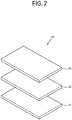
- FIG. 2 illustrates a structure of the display panel 131 according to an exemplary embodiment.
- the display panel 131 includes a substrate 21, a semiconductor layer 22, and a light output layer 23.
- the substrate 21 has a flat panel shape of silicone materials, and the semiconductor layer 22 and the light output layer 23 are stacked on the substrate 21.
- the light output layer 23 outputs light according to control of an electrical driving signal applied by the semiconductor layer 22.
- a type of the light output layer 23 is determined based on a display mode of the display unit 13.
- the light output layer 23 may be configured as a liquid crystal layer.
- the light output layer 23 may be configured as an organic electroluminescence (EL) layer.
- the liquid crystal layer outputs light by selectively transmitting light from a light source unit 72 in FIG. 7 .
- the organic EL layer outputs light by emitting light based on an applied signal.
- the semiconductor layer 22 is arranged in a matrix form corresponding to a plurality of pixels of an image displayed on the display unit 13 and drives the light output layer 23 by receiving a driving signal.
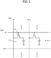
- FIG. 3 illustrates an equivalent circuit of the semiconductor 22 layer according to an exemplary embodiment.
- the semiconductor layer 22 is provided corresponding to each pixel 31 and includes a plurality of switching elements 32 switching based on a driving signal for driving the light output layer 23.
- the switching elements 32 may be configured as a thin film transistor (TFT).
- the semiconductor layer 22 includes a plurality of lines Gn, Gn+1, etc. and Dn, Dn+1, etc. to transmit the driving signal to drive the light output layer 23.
- the driving signal includes a gate signal and a data signal, and the plurality of lines Gn, Gn+i, etc. and Dn, Dn+1, etc. include gate lines Gn, Gn+i, etc. to transmit the gate signal and data lines Dn, Dn+1, etc. to transmit the data signal.
- the display panel 131 further includes a driver circuit (not shown) to output the driving signal to the plurality of lines Gn, Gn+1, etc. and Dn, Dn+1, etc. based on an image signal.
- the display panel 131 may further include a color filter to determine a color of light output from the light output unit 23 and a polarizing layer to polarize the output light.
- FIG. 4 illustrates a gate line according to a related art.
- the gate line 42 in a semiconductor layer 41 has a predetermined width and extends across the semiconductor layer 41.
- the gate line 42 receives a gate signal 43 that is a driving signal from a driver circuit from opposite ends thereof.
- the gate line 42 shown in FIG. 4 has a constant width in a lengthwise direction.
- FIG. 5 illustrates distortion of a gate signal according to a related art.
- the gate signal is gradually influenced by the resistance of the gate line 52 as the gate signal is transmitted from an end portion 53 of the gate line 52 to a central portion 54, waveforms 55, 56 and 57 of the gate signal are more distorted from the end portion 53 of the gate line 52 to the central portion 54.
- the gate signal of the gate line 52 is distorted, difference in charging rate occurs based on a portion of the gate line 52, causing deterioration in image quality.
- FIG. 6 illustrates a gate line according to an exemplary embodiment.
- the gate line 62 of an embodiment has a thickness increasing in a lengthwise direction of the gate line 62 from an end portion 63 to a central portion 64. That is, defining a width of the gate line 62 at the end portion 63 as a, a width thereof at the central portion 64 as c, and a width thereof at a portion between the end portion 63 and the central portion 64 as b.
- the width a is greater than the width b which is greater than the width c as shown in FIG. 6 .
- the thickness of the gate line 62 may be adjusted considering the distortion of the waveform 65 of the gate signal. For example, the thickness of the gate line 62 at the end portion 63 may be 30 to 50% of the width thereof at the central portion 64.
- the pixel regions 66 to 68 refer to an area where light is transmitted through the semiconductor layer 41. As shown in FIG. 6 , the sizes of the pixel regions 66 to 68 gradually decrease from the end portion 63 to the central portion 64. Accordingly, an extent of transmission of light through the semiconductor layer 41 may gradually decrease from the end portion 63 to the central portion 64.
- FIG. 7 illustrates a cross section of the display unit 13 according to an exemplary embodiment.
- the display unit 13 according to an embodiment further includes a light source unit 72 and a light guide plate 73.
- the light source unit 72 provides light to the display panel 131.
- the light source unit 72 may be configured as a fluorescent lamp, a light emitting diode (LED), or the like and be disposed on a lateral side of the light guide plate 73.
- the light guide plate 73 guides light from the light source unit 72 to be transmitted to the display panel 131.
- the light guide plate 73 includes a pattern to refract the light from the light source unit 72 so that the light is evenly transmitted to the display panel 131.
- the pattern may be disposed on a bottom surface 76 of the light guide plate 73 and be formed by various methods, for example, etching and dotting.
- the pattern is provided to compensate for reduction in the extent of transmission of light due to decrease in the sizes of the pixel regions 66 to 68 illustrated in FIG. 6 . That is, the pattern of the light guide plate 73 is provided to increase output brightness of the light guide plate 73 from a region 74 corresponding to the end portion 63 of the gate line 62 to a region 75 corresponding to the central portion 64 of the gate line 62.
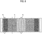
- FIG. 8 is a plan view of a light guide plate 81, viewed from the display panel 131 according to an exemplary embodiment. As shown in FIG. 8 , output brightness of the light guide plate 81 increases from a region 84 corresponding to the end portion 63 of the gate line 62 to a region 86 corresponding to the central portion 64 of the gate line 62.
- FIG. 9 is a graph illustrating a size of a pixel region, output brightness of a light guide plate, and overall transmittance based on a region of the display unit 13.
- A, B, and C refer to regions corresponding to the three portions a, b, and c of the gate line 62 shown in FIG. 6 , respectively.
- the sizes of the pixel regions 66 to 68 gradually decrease (see 91) while the output brightness of the light guide plate 73 gradually increases (see 92).
- a width of a data line may be adjusted.
- the image processing apparatus 12 adjusts brightness of an image based on a region thereof, thereby compensating for the reduction in the extent of light transmittance due to the decrease in the sizes of the pixel regions 66 to 68.
Landscapes
- Physics & Mathematics (AREA)
- Engineering & Computer Science (AREA)
- General Physics & Mathematics (AREA)
- Nonlinear Science (AREA)
- Theoretical Computer Science (AREA)
- Chemical & Material Sciences (AREA)
- Mathematical Physics (AREA)
- Crystallography & Structural Chemistry (AREA)
- Optics & Photonics (AREA)
- Computer Hardware Design (AREA)
- Microelectronics & Electronic Packaging (AREA)
- Devices For Indicating Variable Information By Combining Individual Elements (AREA)
- Electroluminescent Light Sources (AREA)
- Control Of El Displays (AREA)
- Control Of Indicators Other Than Cathode Ray Tubes (AREA)
Claims (5)
- Appareil d'affichage comportant :une unité de traitement d'image (12) configurée pour traiter un signal d'image ; etune unité d'affichage comportant un panneau d'affichage (131) configuré pour afficher une image en fonction du signal d'image,le panneau d'affichage (131) comportant :un substrat (21) ayant une forme de panneau plat ;une couche semi-conductrice (22) comportant une pluralité d'éléments de commutation (32) agencés en une forme de matrice et associés à une pluralité de pixels (31), chaque pixel étant défini par une région de pixels correspondante (66 ; 67 ; 68) qui représente une zone au travers de laquelle de la lumière est transmise, une pluralité de lignes (62) agencées pour s'étendre en travers de la couche semi-conductrice et pour transmettre le signal d'entraînement à la pluralité d'éléments de commutation (32), et une couche d'émission de lumière (23) disposée sur la couche semi-conductrice et émettant de la lumière par un entraînement électrique ; dans lequel les éléments de commutation sont agencés pour effectuer une commutation en fonction d'un signal d'entraînement à des fins d'entraînement de la couche d'émission de lumière (23),dans lequel au moins l'une des lignes (62) a une largeur au niveau d'une partie centrale (64) supérieure aux largeurs au niveau de ses deux extrémités,dans lequel la largeur de ladite au moins l'une des lignes va progressivement en augmentant dans la direction allant dans le sens de la longueur depuis ses deux extrémités jusqu'à la partie centrale (64) de telle sorte que la taille de la région de pixels correspondante va progressivement en diminuant depuis les deux parties d'extrémité jusqu'à la partie centrale, dans lequel ladite au moins l'une des lignes est configurée pour recevoir le signal d'entraînement en provenance des deux extrémités de celle-ci,dans lequel l'unité d'affichage comporte par ailleurs une unité de source de lumière (72) configurée pour fournir de la lumière et une plaque de guidage de lumière (73) configurée pour guider la lumière fournie en provenance de l'unité de source de lumière à des fins d'émission jusque sur le panneau d'affichage, etdans lequel la plaque de guidage de lumière comporte un motif à des fins de compensation des variations au niveau du facteur de transmission de lumière au travers des régions de pixels en raison de la différence de largeur de ladite au moins l'une des lignes.
- Appareil d'affichage comportant :une unité de traitement d'image (12) configurée pour traiter un signal d'image ; etune unité d'affichage comportant un panneau d'affichage (131) configuré pour afficher une image en fonction du signal d'image,le panneau d'affichage (131) comportant :un substrat (21) ayant une forme de panneau plat ;une couche semi-conductrice (22) comportant une pluralité d'éléments de commutation (32) agencés en une forme de matrice et associés à une pluralité de pixels (31), chaque pixel étant défini par une région de pixels correspondante (66 ; 67 ; 68) qui représente une zone au travers de laquelle de la lumière est générée ou transmise,une pluralité de lignes (62) agencées pour s'étendre en travers de la couche semi-conductrice (22) et pour transmettre le signal d'entraînement à la pluralité d'éléments de commutation (32), etune couche d'émission de lumière (23) disposée sur la couche semi-conductrice (22) et émettant de la lumière par un entraînement électrique ;
dans lequelles éléments de commutation (32) sont agencés pour effectuer une commutation en fonction d'un signal d'entraînement à des fins d'entraînement de la couche d'émission de lumière (23),
dans lequelau moins l'une des lignes (62) a une largeur au niveau d'une partie centrale (64) supérieure aux largeurs au niveau de ses deux extrémités,
dans lequella largeur de ladite au moins l'une des lignes va progressivement en augmentant dans la direction allant dans le sens de la longueur depuis ses deux extrémités jusqu'à la partie centrale (64) de telle sorte que la taille de la région de pixels correspondante va progressivement en diminuant depuis les deux parties d'extrémité jusqu'à la partie centrale,
dans lequelladite au moins l'une des lignes est configurée pour recevoir le signal d'entraînement en provenance des deux extrémités de celle-ci, et
dans lequell'unité de traitement d'image est configurée pour émettre le signal d'image avec un ajustement de la luminosité d'une partie correspondante d'une image à des fins de compensation des variations au niveau de la lumière générée par ou transmise au travers des régions de pixels en raison de la différence de largeur de ladite au moins l'une des lignes. - Appareil d'affichage selon la revendication 1 ou la revendication 2, dans lequel le signal d'entraînement comporte un signal de gâchette agencé à des fins d'application sur une gâchette des éléments de commutation, et les lignes comportent une pluralité de lignes à gâchette à des fins de transmission du signal de gâchette.
- Appareil d'affichage selon l'une quelconque des revendications 1 à 3, dans lequel la couche d'émission de lumière comporte une couche de cristaux liquides.
- Appareil d'affichage selon la revendication 2 ou la revendication 3, dans lequel la couche d'émission de lumière comporte une couche électroluminescente organique.
Applications Claiming Priority (1)
| Application Number | Priority Date | Filing Date | Title |
|---|---|---|---|
| KR1020120102037A KR20140035613A (ko) | 2012-09-14 | 2012-09-14 | 디스플레이패널 및 이를 포함하는 디스플레이장치 |
Publications (2)
| Publication Number | Publication Date |
|---|---|
| EP2708942A1 EP2708942A1 (fr) | 2014-03-19 |
| EP2708942B1 true EP2708942B1 (fr) | 2018-01-10 |
Family
ID=48914099
Family Applications (1)
| Application Number | Title | Priority Date | Filing Date |
|---|---|---|---|
| EP13178760.8A Not-in-force EP2708942B1 (fr) | 2012-09-14 | 2013-07-31 | Panneau d'affichage et appareil d'affichage comprenant celui-ci |
Country Status (4)
| Country | Link |
|---|---|
| US (1) | US9196223B2 (fr) |
| EP (1) | EP2708942B1 (fr) |
| KR (1) | KR20140035613A (fr) |
| CN (1) | CN103676372B (fr) |
Families Citing this family (5)
| Publication number | Priority date | Publication date | Assignee | Title |
|---|---|---|---|---|
| US10409102B2 (en) * | 2016-09-08 | 2019-09-10 | Japan Display Inc. | Display device |
| CN107807480B (zh) * | 2016-09-08 | 2021-04-20 | 株式会社日本显示器 | 显示装置 |
| CN106783890A (zh) * | 2017-02-07 | 2017-05-31 | 京东方科技集团股份有限公司 | 一种阵列基板及其制备方法、显示装置 |
| JP7330539B2 (ja) | 2018-03-27 | 2023-08-22 | ナチュールズ デザイン,インコーポレイテッド | 呼吸マスクと共に使用するためのライナ及び保持部材 |
| TWI767654B (zh) * | 2021-04-16 | 2022-06-11 | 友達光電股份有限公司 | 顯示裝置及其驅動方法 |
Citations (2)
| Publication number | Priority date | Publication date | Assignee | Title |
|---|---|---|---|---|
| US5148301A (en) * | 1990-02-27 | 1992-09-15 | Casio Computer Co., Ltd. | Liquid crystal display device having a driving circuit inside the seal boundary |
| US5757450A (en) * | 1994-09-08 | 1998-05-26 | Hitachi, Ltd. | Liquid crystal display with color filters and sizes of inclined linear wiring and terminal electrodes adjusted for equal resistances |
Family Cites Families (12)
| Publication number | Priority date | Publication date | Assignee | Title |
|---|---|---|---|---|
| TW495635B (en) * | 1997-07-11 | 2002-07-21 | Hitachi Ltd | Liquid crystal display device |
| US7164405B1 (en) | 1998-06-27 | 2007-01-16 | Lg.Philips Lcd Co., Ltd. | Method of driving liquid crystal panel and apparatus |
| JP2000338523A (ja) | 1999-05-25 | 2000-12-08 | Nec Corp | 液晶表示装置 |
| US7088323B2 (en) * | 2000-12-21 | 2006-08-08 | Lg.Philips Lcd Co., Ltd. | Liquid crystal display device and method for fabricating the same |
| US6947022B2 (en) | 2002-02-11 | 2005-09-20 | National Semiconductor Corporation | Display line drivers and method for signal propagation delay compensation |
| US7291923B1 (en) * | 2003-07-24 | 2007-11-06 | Xilinx, Inc. | Tapered signal lines |
| JP4086035B2 (ja) * | 2004-12-09 | 2008-05-14 | セイコーエプソン株式会社 | 自動画像補正回路 |
| KR100933455B1 (ko) | 2005-06-27 | 2009-12-23 | 엘지디스플레이 주식회사 | 액정표시장치 |
| KR20080053599A (ko) | 2006-12-11 | 2008-06-16 | 삼성전자주식회사 | 액정 표시 장치 |
| TWI396911B (zh) * | 2008-01-08 | 2013-05-21 | Au Optronics Corp | 畫素結構 |
| US8957926B2 (en) * | 2009-06-11 | 2015-02-17 | Sharp Kabushiki Kaisha | Liquid crystal display apparatus |
| JP5386555B2 (ja) * | 2011-07-28 | 2014-01-15 | 株式会社ジャパンディスプレイ | 液晶表示装置 |
-
2012
- 2012-09-14 KR KR1020120102037A patent/KR20140035613A/ko not_active Ceased
-
2013
- 2013-07-22 US US13/947,497 patent/US9196223B2/en not_active Expired - Fee Related
- 2013-07-31 EP EP13178760.8A patent/EP2708942B1/fr not_active Not-in-force
- 2013-08-13 CN CN201310350085.1A patent/CN103676372B/zh not_active Expired - Fee Related
Patent Citations (2)
| Publication number | Priority date | Publication date | Assignee | Title |
|---|---|---|---|---|
| US5148301A (en) * | 1990-02-27 | 1992-09-15 | Casio Computer Co., Ltd. | Liquid crystal display device having a driving circuit inside the seal boundary |
| US5757450A (en) * | 1994-09-08 | 1998-05-26 | Hitachi, Ltd. | Liquid crystal display with color filters and sizes of inclined linear wiring and terminal electrodes adjusted for equal resistances |
Also Published As
| Publication number | Publication date |
|---|---|
| KR20140035613A (ko) | 2014-03-24 |
| EP2708942A1 (fr) | 2014-03-19 |
| US20140078027A1 (en) | 2014-03-20 |
| US9196223B2 (en) | 2015-11-24 |
| CN103676372A (zh) | 2014-03-26 |
| CN103676372B (zh) | 2018-06-08 |
Similar Documents
| Publication | Publication Date | Title |
|---|---|---|
| KR102082779B1 (ko) | 플렉서블 디스플레이 장치 및 그 제어 방법 | |
| US8228263B2 (en) | Stacked LCD unit | |
| US10062334B2 (en) | Backlight dimming control for a display utilizing quantum dots | |
| US9208709B2 (en) | Backlight for a display | |
| US20080238860A1 (en) | Liquid crystal display apparatus | |
| KR101656742B1 (ko) | 액정표시장치 | |
| EP2708942B1 (fr) | Panneau d'affichage et appareil d'affichage comprenant celui-ci | |
| US10714036B2 (en) | Electronic device, display device and display control method | |
| US10210786B2 (en) | Display device, method of driving display device, and electronic device having display device | |
| JP4292242B2 (ja) | 帰還回路部を備えた液晶表示装置 | |
| JP4799061B2 (ja) | 液晶表示装置及びその駆動方法 | |
| JP2011203322A (ja) | 液晶表示装置 | |
| US8848003B2 (en) | Method of chromaticity adjustment of display device | |
| US9653027B2 (en) | Display apparatus | |
| KR101633113B1 (ko) | 액정표시장치 | |
| KR102404464B1 (ko) | 액정 디스플레이 장치 및 이의 구동 방법 | |
| KR101787745B1 (ko) | 액정표시장치 | |
| US20110234938A1 (en) | Display apparatus and backlight unit | |
| US20160365038A1 (en) | Display panel and display apparatus | |
| US20120120125A1 (en) | Lcd apparatus and method for compensating temperature | |
| KR20200057256A (ko) | 디스플레이 장치 및 그 구동 방법 | |
| KR102146829B1 (ko) | 표시 장치 | |
| US10255838B2 (en) | Semiconductor device and electronic device | |
| KR102408806B1 (ko) | 액정 디스플레이 장치 및 이의 구동 방법 | |
| JP4732070B2 (ja) | フィードフォワード回路部が具備される液晶表示装置 |
Legal Events
| Date | Code | Title | Description |
|---|---|---|---|
| PUAI | Public reference made under article 153(3) epc to a published international application that has entered the european phase |
Free format text: ORIGINAL CODE: 0009012 |
|
| AK | Designated contracting states |
Kind code of ref document: A1 Designated state(s): AL AT BE BG CH CY CZ DE DK EE ES FI FR GB GR HR HU IE IS IT LI LT LU LV MC MK MT NL NO PL PT RO RS SE SI SK SM TR |
|
| AX | Request for extension of the european patent |
Extension state: BA ME |
|
| 17P | Request for examination filed |
Effective date: 20140918 |
|
| RBV | Designated contracting states (corrected) |
Designated state(s): AL AT BE BG CH CY CZ DE DK EE ES FI FR GB GR HR HU IE IS IT LI LT LU LV MC MK MT NL NO PL PT RO RS SE SI SK SM TR |
|
| 17Q | First examination report despatched |
Effective date: 20150611 |
|
| STAA | Information on the status of an ep patent application or granted ep patent |
Free format text: STATUS: EXAMINATION IS IN PROGRESS |
|
| GRAP | Despatch of communication of intention to grant a patent |
Free format text: ORIGINAL CODE: EPIDOSNIGR1 |
|
| STAA | Information on the status of an ep patent application or granted ep patent |
Free format text: STATUS: GRANT OF PATENT IS INTENDED |
|
| INTG | Intention to grant announced |
Effective date: 20170926 |
|
| GRAS | Grant fee paid |
Free format text: ORIGINAL CODE: EPIDOSNIGR3 |
|
| GRAA | (expected) grant |
Free format text: ORIGINAL CODE: 0009210 |
|
| STAA | Information on the status of an ep patent application or granted ep patent |
Free format text: STATUS: THE PATENT HAS BEEN GRANTED |
|
| RAP1 | Party data changed (applicant data changed or rights of an application transferred) |
Owner name: SAMSUNG ELECTRONICS CO., LTD. |
|
| AK | Designated contracting states |
Kind code of ref document: B1 Designated state(s): AL AT BE BG CH CY CZ DE DK EE ES FI FR GB GR HR HU IE IS IT LI LT LU LV MC MK MT NL NO PL PT RO RS SE SI SK SM TR |
|
| REG | Reference to a national code |
Ref country code: CH Ref legal event code: EP Ref country code: AT Ref legal event code: REF Ref document number: 963020 Country of ref document: AT Kind code of ref document: T Effective date: 20180115 |
|
| REG | Reference to a national code |
Ref country code: IE Ref legal event code: FG4D |
|
| REG | Reference to a national code |
Ref country code: DE Ref legal event code: R096 Ref document number: 602013032034 Country of ref document: DE |
|
| REG | Reference to a national code |
Ref country code: NL Ref legal event code: MP Effective date: 20180110 |
|
| REG | Reference to a national code |
Ref country code: AT Ref legal event code: MK05 Ref document number: 963020 Country of ref document: AT Kind code of ref document: T Effective date: 20180110 |
|
| PG25 | Lapsed in a contracting state [announced via postgrant information from national office to epo] |
Ref country code: NL Free format text: LAPSE BECAUSE OF FAILURE TO SUBMIT A TRANSLATION OF THE DESCRIPTION OR TO PAY THE FEE WITHIN THE PRESCRIBED TIME-LIMIT Effective date: 20180110 |
|
| PG25 | Lapsed in a contracting state [announced via postgrant information from national office to epo] |
Ref country code: ES Free format text: LAPSE BECAUSE OF FAILURE TO SUBMIT A TRANSLATION OF THE DESCRIPTION OR TO PAY THE FEE WITHIN THE PRESCRIBED TIME-LIMIT Effective date: 20180110 Ref country code: LT Free format text: LAPSE BECAUSE OF FAILURE TO SUBMIT A TRANSLATION OF THE DESCRIPTION OR TO PAY THE FEE WITHIN THE PRESCRIBED TIME-LIMIT Effective date: 20180110 Ref country code: NO Free format text: LAPSE BECAUSE OF FAILURE TO SUBMIT A TRANSLATION OF THE DESCRIPTION OR TO PAY THE FEE WITHIN THE PRESCRIBED TIME-LIMIT Effective date: 20180410 Ref country code: CY Free format text: LAPSE BECAUSE OF FAILURE TO SUBMIT A TRANSLATION OF THE DESCRIPTION OR TO PAY THE FEE WITHIN THE PRESCRIBED TIME-LIMIT Effective date: 20180110 Ref country code: HR Free format text: LAPSE BECAUSE OF FAILURE TO SUBMIT A TRANSLATION OF THE DESCRIPTION OR TO PAY THE FEE WITHIN THE PRESCRIBED TIME-LIMIT Effective date: 20180110 Ref country code: FI Free format text: LAPSE BECAUSE OF FAILURE TO SUBMIT A TRANSLATION OF THE DESCRIPTION OR TO PAY THE FEE WITHIN THE PRESCRIBED TIME-LIMIT Effective date: 20180110 |
|
| PG25 | Lapsed in a contracting state [announced via postgrant information from national office to epo] |
Ref country code: IS Free format text: LAPSE BECAUSE OF FAILURE TO SUBMIT A TRANSLATION OF THE DESCRIPTION OR TO PAY THE FEE WITHIN THE PRESCRIBED TIME-LIMIT Effective date: 20180510 Ref country code: PL Free format text: LAPSE BECAUSE OF FAILURE TO SUBMIT A TRANSLATION OF THE DESCRIPTION OR TO PAY THE FEE WITHIN THE PRESCRIBED TIME-LIMIT Effective date: 20180110 Ref country code: RS Free format text: LAPSE BECAUSE OF FAILURE TO SUBMIT A TRANSLATION OF THE DESCRIPTION OR TO PAY THE FEE WITHIN THE PRESCRIBED TIME-LIMIT Effective date: 20180110 Ref country code: SE Free format text: LAPSE BECAUSE OF FAILURE TO SUBMIT A TRANSLATION OF THE DESCRIPTION OR TO PAY THE FEE WITHIN THE PRESCRIBED TIME-LIMIT Effective date: 20180110 Ref country code: LV Free format text: LAPSE BECAUSE OF FAILURE TO SUBMIT A TRANSLATION OF THE DESCRIPTION OR TO PAY THE FEE WITHIN THE PRESCRIBED TIME-LIMIT Effective date: 20180110 Ref country code: AT Free format text: LAPSE BECAUSE OF FAILURE TO SUBMIT A TRANSLATION OF THE DESCRIPTION OR TO PAY THE FEE WITHIN THE PRESCRIBED TIME-LIMIT Effective date: 20180110 Ref country code: GR Free format text: LAPSE BECAUSE OF FAILURE TO SUBMIT A TRANSLATION OF THE DESCRIPTION OR TO PAY THE FEE WITHIN THE PRESCRIBED TIME-LIMIT Effective date: 20180411 Ref country code: BG Free format text: LAPSE BECAUSE OF FAILURE TO SUBMIT A TRANSLATION OF THE DESCRIPTION OR TO PAY THE FEE WITHIN THE PRESCRIBED TIME-LIMIT Effective date: 20180410 |
|
| REG | Reference to a national code |
Ref country code: DE Ref legal event code: R097 Ref document number: 602013032034 Country of ref document: DE |
|
| PG25 | Lapsed in a contracting state [announced via postgrant information from national office to epo] |
Ref country code: RO Free format text: LAPSE BECAUSE OF FAILURE TO SUBMIT A TRANSLATION OF THE DESCRIPTION OR TO PAY THE FEE WITHIN THE PRESCRIBED TIME-LIMIT Effective date: 20180110 Ref country code: AL Free format text: LAPSE BECAUSE OF FAILURE TO SUBMIT A TRANSLATION OF THE DESCRIPTION OR TO PAY THE FEE WITHIN THE PRESCRIBED TIME-LIMIT Effective date: 20180110 Ref country code: EE Free format text: LAPSE BECAUSE OF FAILURE TO SUBMIT A TRANSLATION OF THE DESCRIPTION OR TO PAY THE FEE WITHIN THE PRESCRIBED TIME-LIMIT Effective date: 20180110 Ref country code: IT Free format text: LAPSE BECAUSE OF FAILURE TO SUBMIT A TRANSLATION OF THE DESCRIPTION OR TO PAY THE FEE WITHIN THE PRESCRIBED TIME-LIMIT Effective date: 20180110 |
|
| PGFP | Annual fee paid to national office [announced via postgrant information from national office to epo] |
Ref country code: DE Payment date: 20180620 Year of fee payment: 6 Ref country code: GB Payment date: 20180621 Year of fee payment: 6 |
|
| PLBE | No opposition filed within time limit |
Free format text: ORIGINAL CODE: 0009261 |
|
| STAA | Information on the status of an ep patent application or granted ep patent |
Free format text: STATUS: NO OPPOSITION FILED WITHIN TIME LIMIT |
|
| PG25 | Lapsed in a contracting state [announced via postgrant information from national office to epo] |
Ref country code: DK Free format text: LAPSE BECAUSE OF FAILURE TO SUBMIT A TRANSLATION OF THE DESCRIPTION OR TO PAY THE FEE WITHIN THE PRESCRIBED TIME-LIMIT Effective date: 20180110 Ref country code: SM Free format text: LAPSE BECAUSE OF FAILURE TO SUBMIT A TRANSLATION OF THE DESCRIPTION OR TO PAY THE FEE WITHIN THE PRESCRIBED TIME-LIMIT Effective date: 20180110 Ref country code: SK Free format text: LAPSE BECAUSE OF FAILURE TO SUBMIT A TRANSLATION OF THE DESCRIPTION OR TO PAY THE FEE WITHIN THE PRESCRIBED TIME-LIMIT Effective date: 20180110 Ref country code: CZ Free format text: LAPSE BECAUSE OF FAILURE TO SUBMIT A TRANSLATION OF THE DESCRIPTION OR TO PAY THE FEE WITHIN THE PRESCRIBED TIME-LIMIT Effective date: 20180110 |
|
| 26N | No opposition filed |
Effective date: 20181011 |
|
| PG25 | Lapsed in a contracting state [announced via postgrant information from national office to epo] |
Ref country code: SI Free format text: LAPSE BECAUSE OF FAILURE TO SUBMIT A TRANSLATION OF THE DESCRIPTION OR TO PAY THE FEE WITHIN THE PRESCRIBED TIME-LIMIT Effective date: 20180110 |
|
| REG | Reference to a national code |
Ref country code: CH Ref legal event code: PL |
|
| PG25 | Lapsed in a contracting state [announced via postgrant information from national office to epo] |
Ref country code: LU Free format text: LAPSE BECAUSE OF NON-PAYMENT OF DUE FEES Effective date: 20180731 Ref country code: MC Free format text: LAPSE BECAUSE OF FAILURE TO SUBMIT A TRANSLATION OF THE DESCRIPTION OR TO PAY THE FEE WITHIN THE PRESCRIBED TIME-LIMIT Effective date: 20180110 |
|
| REG | Reference to a national code |
Ref country code: BE Ref legal event code: MM Effective date: 20180731 |
|
| PG25 | Lapsed in a contracting state [announced via postgrant information from national office to epo] |
Ref country code: LI Free format text: LAPSE BECAUSE OF NON-PAYMENT OF DUE FEES Effective date: 20180731 Ref country code: CH Free format text: LAPSE BECAUSE OF NON-PAYMENT OF DUE FEES Effective date: 20180731 Ref country code: FR Free format text: LAPSE BECAUSE OF NON-PAYMENT OF DUE FEES Effective date: 20180731 |
|
| REG | Reference to a national code |
Ref country code: IE Ref legal event code: MM4A |
|
| PG25 | Lapsed in a contracting state [announced via postgrant information from national office to epo] |
Ref country code: BE Free format text: LAPSE BECAUSE OF NON-PAYMENT OF DUE FEES Effective date: 20180731 |
|
| PG25 | Lapsed in a contracting state [announced via postgrant information from national office to epo] |
Ref country code: IE Free format text: LAPSE BECAUSE OF NON-PAYMENT OF DUE FEES Effective date: 20180731 |
|
| PG25 | Lapsed in a contracting state [announced via postgrant information from national office to epo] |
Ref country code: MT Free format text: LAPSE BECAUSE OF NON-PAYMENT OF DUE FEES Effective date: 20180731 |
|
| REG | Reference to a national code |
Ref country code: DE Ref legal event code: R119 Ref document number: 602013032034 Country of ref document: DE |
|
| GBPC | Gb: european patent ceased through non-payment of renewal fee |
Effective date: 20190731 |
|
| PG25 | Lapsed in a contracting state [announced via postgrant information from national office to epo] |
Ref country code: TR Free format text: LAPSE BECAUSE OF FAILURE TO SUBMIT A TRANSLATION OF THE DESCRIPTION OR TO PAY THE FEE WITHIN THE PRESCRIBED TIME-LIMIT Effective date: 20180110 |
|
| PG25 | Lapsed in a contracting state [announced via postgrant information from national office to epo] |
Ref country code: DE Free format text: LAPSE BECAUSE OF NON-PAYMENT OF DUE FEES Effective date: 20200201 Ref country code: GB Free format text: LAPSE BECAUSE OF NON-PAYMENT OF DUE FEES Effective date: 20190731 |
|
| PG25 | Lapsed in a contracting state [announced via postgrant information from national office to epo] |
Ref country code: PT Free format text: LAPSE BECAUSE OF FAILURE TO SUBMIT A TRANSLATION OF THE DESCRIPTION OR TO PAY THE FEE WITHIN THE PRESCRIBED TIME-LIMIT Effective date: 20180110 Ref country code: HU Free format text: LAPSE BECAUSE OF FAILURE TO SUBMIT A TRANSLATION OF THE DESCRIPTION OR TO PAY THE FEE WITHIN THE PRESCRIBED TIME-LIMIT; INVALID AB INITIO Effective date: 20130731 |
|
| PG25 | Lapsed in a contracting state [announced via postgrant information from national office to epo] |
Ref country code: MK Free format text: LAPSE BECAUSE OF NON-PAYMENT OF DUE FEES Effective date: 20180110 |