EP2711151A1 - Procédé de fabrication de wafers - Google Patents
Procédé de fabrication de wafers Download PDFInfo
- Publication number
- EP2711151A1 EP2711151A1 EP12185757.7A EP12185757A EP2711151A1 EP 2711151 A1 EP2711151 A1 EP 2711151A1 EP 12185757 A EP12185757 A EP 12185757A EP 2711151 A1 EP2711151 A1 EP 2711151A1
- Authority
- EP
- European Patent Office
- Prior art keywords
- gluing
- wafers
- fluid
- cutting
- wire
- Prior art date
- Legal status (The legal status is an assumption and is not a legal conclusion. Google has not performed a legal analysis and makes no representation as to the accuracy of the status listed.)
- Withdrawn
Links
- 235000012431 wafers Nutrition 0.000 title claims abstract description 128
- 238000004519 manufacturing process Methods 0.000 title claims abstract description 7
- 238000004026 adhesive bonding Methods 0.000 claims abstract description 152
- 239000012530 fluid Substances 0.000 claims abstract description 89
- 238000005520 cutting process Methods 0.000 claims abstract description 52
- 238000000034 method Methods 0.000 claims abstract description 27
- 238000004140 cleaning Methods 0.000 claims description 31
- 239000002173 cutting fluid Substances 0.000 claims description 7
- 230000008961 swelling Effects 0.000 claims description 7
- 239000002904 solvent Substances 0.000 claims description 5
- 239000011358 absorbing material Substances 0.000 claims description 3
- 239000003292 glue Substances 0.000 description 9
- 239000000853 adhesive Substances 0.000 description 5
- 230000001070 adhesive effect Effects 0.000 description 5
- 230000033001 locomotion Effects 0.000 description 5
- 239000000463 material Substances 0.000 description 5
- 239000002002 slurry Substances 0.000 description 5
- XLYOFNOQVPJJNP-UHFFFAOYSA-N water Substances O XLYOFNOQVPJJNP-UHFFFAOYSA-N 0.000 description 5
- 239000011449 brick Substances 0.000 description 4
- 230000000694 effects Effects 0.000 description 4
- 238000010438 heat treatment Methods 0.000 description 4
- 239000002184 metal Substances 0.000 description 4
- 238000000926 separation method Methods 0.000 description 4
- 239000003082 abrasive agent Substances 0.000 description 3
- 238000009826 distribution Methods 0.000 description 3
- 239000007788 liquid Substances 0.000 description 3
- 238000009827 uniform distribution Methods 0.000 description 3
- XUIMIQQOPSSXEZ-UHFFFAOYSA-N Silicon Chemical compound [Si] XUIMIQQOPSSXEZ-UHFFFAOYSA-N 0.000 description 2
- 230000004888 barrier function Effects 0.000 description 2
- 238000006243 chemical reaction Methods 0.000 description 2
- 239000002178 crystalline material Substances 0.000 description 2
- 239000011521 glass Substances 0.000 description 2
- 238000011065 in-situ storage Methods 0.000 description 2
- 239000000758 substrate Substances 0.000 description 2
- 230000001419 dependent effect Effects 0.000 description 1
- 229910003460 diamond Inorganic materials 0.000 description 1
- 239000010432 diamond Substances 0.000 description 1
- 238000005516 engineering process Methods 0.000 description 1
- 238000011010 flushing procedure Methods 0.000 description 1
- 230000003993 interaction Effects 0.000 description 1
- 230000001788 irregular Effects 0.000 description 1
- 238000002844 melting Methods 0.000 description 1
- 230000008018 melting Effects 0.000 description 1
- 239000002245 particle Substances 0.000 description 1
- 230000006798 recombination Effects 0.000 description 1
- 238000005215 recombination Methods 0.000 description 1
- 229910052594 sapphire Inorganic materials 0.000 description 1
- 239000010980 sapphire Substances 0.000 description 1
- 239000004065 semiconductor Substances 0.000 description 1
- 230000035939 shock Effects 0.000 description 1
- 229910052710 silicon Inorganic materials 0.000 description 1
- 239000010703 silicon Substances 0.000 description 1
- 239000011856 silicon-based particle Substances 0.000 description 1
- 238000010792 warming Methods 0.000 description 1
Images


Classifications
-
- B—PERFORMING OPERATIONS; TRANSPORTING
- B28—WORKING CEMENT, CLAY, OR STONE
- B28D—WORKING STONE OR STONE-LIKE MATERIALS
- B28D5/00—Fine working of gems, jewels, crystals, e.g. of semiconductor material; apparatus or devices therefor
- B28D5/0058—Accessories specially adapted for use with machines for fine working of gems, jewels, crystals, e.g. of semiconductor material
- B28D5/0082—Accessories specially adapted for use with machines for fine working of gems, jewels, crystals, e.g. of semiconductor material for supporting, holding, feeding, conveying or discharging work
Definitions
- heat of the cutting wire is efficiently transmitted to the gluing layer (adding heat from the wires). Since the wires are warm themselves during the cutting process, they may be placed just below the gluing layer to be dissolved so that their warmth deteriorates the glue as well (additionally to the effect of the de-gluing fluid).
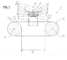
- Fig. 1 shows a wire saw 2 for cutting a plurality of wafers from an ingot 4 (also called brick or core).
- the wire saw 2 comprises a support base 21 for positioning ingot 4 with respect to a wire web 18 which is formed by a cutting wire.
- Ingot 4 is by gluing attached to a beam 19 (also called sacrificial substrate), which in turn is attached to a fixture attachment 20 usually made of metal.
- the beam 19 is mounted to the fixture attachment 20 which in turn is detachably mounted to the support base 21 of the wire saw 2.
- the ingot 4 is pushed through the wire web 18, causing the cutting wire to bend downwards (not shown). Because of this bow of the cutting wire, the top edges of the ingot are cut before the middle part of the ingot is completely cut. It is the purpose of the sacrificial substrate or beam 19 to keep the fixture attachment 20 at a distance of the ingot 4, so that the fixture attachment 20 is not cut.
- the beam 19 - which is relatively inexpensive - is replaced after each cut.
- the de-gluing fluid 7 may be a heated cutting fluid also used for/during the cutting step to wet the wire web 18.
Landscapes
- Engineering & Computer Science (AREA)
- Mechanical Engineering (AREA)
- Processing Of Stones Or Stones Resemblance Materials (AREA)
- Mechanical Treatment Of Semiconductor (AREA)
- Finish Polishing, Edge Sharpening, And Grinding By Specific Grinding Devices (AREA)
Priority Applications (3)
| Application Number | Priority Date | Filing Date | Title |
|---|---|---|---|
| EP12185757.7A EP2711151A1 (fr) | 2012-09-24 | 2012-09-24 | Procédé de fabrication de wafers |
| TW102134028A TW201429662A (zh) | 2012-09-24 | 2013-09-23 | 晶圓製造方法 |
| PCT/IB2013/002093 WO2014045108A1 (fr) | 2012-09-24 | 2013-09-23 | Procédé de fabrication de plaquettes |
Applications Claiming Priority (1)
| Application Number | Priority Date | Filing Date | Title |
|---|---|---|---|
| EP12185757.7A EP2711151A1 (fr) | 2012-09-24 | 2012-09-24 | Procédé de fabrication de wafers |
Publications (1)
| Publication Number | Publication Date |
|---|---|
| EP2711151A1 true EP2711151A1 (fr) | 2014-03-26 |
Family
ID=47143518
Family Applications (1)
| Application Number | Title | Priority Date | Filing Date |
|---|---|---|---|
| EP12185757.7A Withdrawn EP2711151A1 (fr) | 2012-09-24 | 2012-09-24 | Procédé de fabrication de wafers |
Country Status (3)
| Country | Link |
|---|---|
| EP (1) | EP2711151A1 (fr) |
| TW (1) | TW201429662A (fr) |
| WO (1) | WO2014045108A1 (fr) |
Cited By (2)
| Publication number | Priority date | Publication date | Assignee | Title |
|---|---|---|---|---|
| TWI777451B (zh) * | 2021-03-15 | 2022-09-11 | 環球晶圓股份有限公司 | 晶棒切片裝置及晶棒切片方法 |
| WO2022218843A1 (fr) * | 2021-04-15 | 2022-10-20 | Fraunhofer-Gesellschaft zur Förderung der angewandten Forschung e. V. | Procédé de fixation d'un bloc de matériau pour l'usinage mécanique |
Citations (14)
| Publication number | Priority date | Publication date | Assignee | Title |
|---|---|---|---|---|
| JPH07153724A (ja) | 1993-11-29 | 1995-06-16 | Sharp Corp | シリコンインゴットのスライス加工方法 |
| JPH0919921A (ja) | 1995-07-07 | 1997-01-21 | Tokyo Seimitsu Co Ltd | ワイヤソー |
| JPH09207126A (ja) | 1996-01-31 | 1997-08-12 | Nippei Toyama Corp | ワイヤソーのためのワーク支持装置、清浄方法及びワイヤソー |
| DE19900671C2 (de) | 1999-01-11 | 2002-04-25 | Fraunhofer Ges Forschung | Verfahren und Vorrichtung zum Vereinzeln von scheibenförmigen Substraten, insbesondere zur Waferherstellung |
| DE102004058194A1 (de) | 2004-12-02 | 2005-08-11 | Siltronic Ag | Sägeleiste und Verfahren zum Abtrennen von Halbleiterscheiben von einem Kristallstück |
| DE102005028112A1 (de) * | 2005-06-13 | 2006-12-21 | Schmid Technology Systems Gmbh | Verfahren zur Positionierung und Lageerhaltung von Substraten, insbesondere von dünnen Siliziumwafern nach dem Drahtsägen zu deren Vereinzelung |
| EP2110216A1 (fr) | 2008-04-14 | 2009-10-21 | Applied Materials, Inc. | Dispositif de scie à fil et son procédé de fonctionnement |
| EP2153960A2 (fr) | 2008-08-14 | 2010-02-17 | Wacker Schott Solar Gmbh | Support, procédé et dispositif de fabrication de tranches de silicium, ainsi que l'utilisation de la tranche de silicium fabriquée |
| WO2010133682A1 (fr) | 2009-05-22 | 2010-11-25 | Gebr. Schmid Gmbh & Co. | Support pour un lingot de silicium |
| WO2011009927A1 (fr) | 2009-07-23 | 2011-01-27 | Gebr. Schmid Gmbh & Co. | Dispositif de nettoyage de substrats sur un support |
| WO2011009917A2 (fr) | 2009-07-23 | 2011-01-27 | Gebr. Schmid Gmbh & Co. | Procédé et dispositif pour nettoyer des substrats sur un support |
| DE102010050897A1 (de) | 2010-07-09 | 2012-01-12 | Interpane Entwicklungs-Und Beratungsgesellschaft Mbh | Trägervorrichtung und Verfahren zum Schneiden eines an der Trägervorrichtung befestigten Materialblocks |
| WO2012007381A1 (fr) | 2010-07-15 | 2012-01-19 | Gebr. Schmid Gmbh & Co. | Support pour bloc de silicium, ensemble support comprenant ce support et procédé de fabrication de cet ensemble support |
| DE102010052635A1 (de) | 2010-11-29 | 2012-05-31 | Rena Gmbh | Halte-Reinigungsvorrichtung und Verfahren zum abschnittsweisen Reinigen gesägter Wafer |
-
2012
- 2012-09-24 EP EP12185757.7A patent/EP2711151A1/fr not_active Withdrawn
-
2013
- 2013-09-23 WO PCT/IB2013/002093 patent/WO2014045108A1/fr not_active Ceased
- 2013-09-23 TW TW102134028A patent/TW201429662A/zh unknown
Patent Citations (14)
| Publication number | Priority date | Publication date | Assignee | Title |
|---|---|---|---|---|
| JPH07153724A (ja) | 1993-11-29 | 1995-06-16 | Sharp Corp | シリコンインゴットのスライス加工方法 |
| JPH0919921A (ja) | 1995-07-07 | 1997-01-21 | Tokyo Seimitsu Co Ltd | ワイヤソー |
| JPH09207126A (ja) | 1996-01-31 | 1997-08-12 | Nippei Toyama Corp | ワイヤソーのためのワーク支持装置、清浄方法及びワイヤソー |
| DE19900671C2 (de) | 1999-01-11 | 2002-04-25 | Fraunhofer Ges Forschung | Verfahren und Vorrichtung zum Vereinzeln von scheibenförmigen Substraten, insbesondere zur Waferherstellung |
| DE102004058194A1 (de) | 2004-12-02 | 2005-08-11 | Siltronic Ag | Sägeleiste und Verfahren zum Abtrennen von Halbleiterscheiben von einem Kristallstück |
| DE102005028112A1 (de) * | 2005-06-13 | 2006-12-21 | Schmid Technology Systems Gmbh | Verfahren zur Positionierung und Lageerhaltung von Substraten, insbesondere von dünnen Siliziumwafern nach dem Drahtsägen zu deren Vereinzelung |
| EP2110216A1 (fr) | 2008-04-14 | 2009-10-21 | Applied Materials, Inc. | Dispositif de scie à fil et son procédé de fonctionnement |
| EP2153960A2 (fr) | 2008-08-14 | 2010-02-17 | Wacker Schott Solar Gmbh | Support, procédé et dispositif de fabrication de tranches de silicium, ainsi que l'utilisation de la tranche de silicium fabriquée |
| WO2010133682A1 (fr) | 2009-05-22 | 2010-11-25 | Gebr. Schmid Gmbh & Co. | Support pour un lingot de silicium |
| WO2011009927A1 (fr) | 2009-07-23 | 2011-01-27 | Gebr. Schmid Gmbh & Co. | Dispositif de nettoyage de substrats sur un support |
| WO2011009917A2 (fr) | 2009-07-23 | 2011-01-27 | Gebr. Schmid Gmbh & Co. | Procédé et dispositif pour nettoyer des substrats sur un support |
| DE102010050897A1 (de) | 2010-07-09 | 2012-01-12 | Interpane Entwicklungs-Und Beratungsgesellschaft Mbh | Trägervorrichtung und Verfahren zum Schneiden eines an der Trägervorrichtung befestigten Materialblocks |
| WO2012007381A1 (fr) | 2010-07-15 | 2012-01-19 | Gebr. Schmid Gmbh & Co. | Support pour bloc de silicium, ensemble support comprenant ce support et procédé de fabrication de cet ensemble support |
| DE102010052635A1 (de) | 2010-11-29 | 2012-05-31 | Rena Gmbh | Halte-Reinigungsvorrichtung und Verfahren zum abschnittsweisen Reinigen gesägter Wafer |
Cited By (2)
| Publication number | Priority date | Publication date | Assignee | Title |
|---|---|---|---|---|
| TWI777451B (zh) * | 2021-03-15 | 2022-09-11 | 環球晶圓股份有限公司 | 晶棒切片裝置及晶棒切片方法 |
| WO2022218843A1 (fr) * | 2021-04-15 | 2022-10-20 | Fraunhofer-Gesellschaft zur Förderung der angewandten Forschung e. V. | Procédé de fixation d'un bloc de matériau pour l'usinage mécanique |
Also Published As
| Publication number | Publication date |
|---|---|
| TW201429662A (zh) | 2014-08-01 |
| WO2014045108A1 (fr) | 2014-03-27 |
Similar Documents
| Publication | Publication Date | Title |
|---|---|---|
| US8261730B2 (en) | In-situ wafer processing system and method | |
| KR100902626B1 (ko) | 공작물의 쏘잉 방법 및 장치 | |
| CN204658729U (zh) | 晶片清洁系统和丝锯 | |
| TWI278027B (en) | Substrate slicing method | |
| CN1816908B (zh) | 芯片焊接 | |
| KR101408552B1 (ko) | 박형 실리콘 로드의 제조를 위한 방법 및 장치 | |
| KR20160032678A (ko) | SiC 잉곳의 슬라이스 방법 | |
| KR101916518B1 (ko) | 기판 처리 방법 | |
| WO2010058389A1 (fr) | Procédé et dispositif pour faciliter la séparation de gaufrettes tranchées | |
| TW200950909A (en) | Mounting plate for a wire sawing device, wire sawing device comprising the same, and wire sawing process carried out by the device | |
| TW201101525A (en) | Method for manufacturing integrated thin-film solar cell | |
| EP2711151A1 (fr) | Procédé de fabrication de wafers | |
| KR102163438B1 (ko) | 절삭 방법 | |
| TWI589419B (zh) | 載體裝置以及將固定在此載體裝置上的材料塊切割的方法 | |
| TWI742276B (zh) | 晶片的製造方法 | |
| TWI485760B (zh) | 將薄片特別是晶圓從脆材料切離的方法與裝置 | |
| JPH10340869A (ja) | マルチ切断ワイヤソーのウェーハ回収方法 | |
| JP6325175B2 (ja) | 平行化切断ビームを用いて超硬度材料のプレートを作製する方法 | |
| EP2711978A1 (fr) | Méthode de fabrication de plaquettes | |
| CN104183476B (zh) | 切削残余部除去装置 | |
| CN113574646A (zh) | 用于碎裂多个晶圆组件的系统 | |
| JP3716555B2 (ja) | マルチ切断ワイヤソーの被加工物切断方法 | |
| JP2003146678A (ja) | 脆性材料の切断方法及び切断装置 | |
| CN102875011A (zh) | 石英晶片化砣装置 | |
| RU2429964C1 (ru) | Способ проволочной резки кремниевого слитка на пластины |
Legal Events
| Date | Code | Title | Description |
|---|---|---|---|
| PUAI | Public reference made under article 153(3) epc to a published international application that has entered the european phase |
Free format text: ORIGINAL CODE: 0009012 |
|
| AK | Designated contracting states |
Kind code of ref document: A1 Designated state(s): AL AT BE BG CH CY CZ DE DK EE ES FI FR GB GR HR HU IE IS IT LI LT LU LV MC MK MT NL NO PL PT RO RS SE SI SK SM TR |
|
| AX | Request for extension of the european patent |
Extension state: BA ME |
|
| STAA | Information on the status of an ep patent application or granted ep patent |
Free format text: STATUS: THE APPLICATION IS DEEMED TO BE WITHDRAWN |
|
| 18D | Application deemed to be withdrawn |
Effective date: 20140929 |