EP2717451A2 - Resonante Gleichstromversorgungsvorrichtung und Steuerverfahren dafür - Google Patents
Resonante Gleichstromversorgungsvorrichtung und Steuerverfahren dafür Download PDFInfo
- Publication number
- EP2717451A2 EP2717451A2 EP13183083.8A EP13183083A EP2717451A2 EP 2717451 A2 EP2717451 A2 EP 2717451A2 EP 13183083 A EP13183083 A EP 13183083A EP 2717451 A2 EP2717451 A2 EP 2717451A2
- Authority
- EP
- European Patent Office
- Prior art keywords
- resonant
- voltage
- circuit
- output
- current
- Prior art date
- Legal status (The legal status is an assumption and is not a legal conclusion. Google has not performed a legal analysis and makes no representation as to the accuracy of the status listed.)
- Granted
Links
Images



Classifications
-
- H—ELECTRICITY
- H02—GENERATION; CONVERSION OR DISTRIBUTION OF ELECTRIC POWER
- H02M—APPARATUS FOR CONVERSION BETWEEN AC AND AC, BETWEEN AC AND DC, OR BETWEEN DC AND DC, AND FOR USE WITH MAINS OR SIMILAR POWER SUPPLY SYSTEMS; CONVERSION OF DC OR AC INPUT POWER INTO SURGE OUTPUT POWER; CONTROL OR REGULATION THEREOF
- H02M3/00—Conversion of DC power input into DC power output
- H02M3/22—Conversion of DC power input into DC power output with intermediate conversion into AC
- H02M3/24—Conversion of DC power input into DC power output with intermediate conversion into AC by static converters
- H02M3/28—Conversion of DC power input into DC power output with intermediate conversion into AC by static converters using discharge tubes with control electrode or semiconductor devices with control electrode to produce the intermediate AC
- H02M3/325—Conversion of DC power input into DC power output with intermediate conversion into AC by static converters using discharge tubes with control electrode or semiconductor devices with control electrode to produce the intermediate AC using devices of a triode or a transistor type requiring continuous application of a control signal
- H02M3/335—Conversion of DC power input into DC power output with intermediate conversion into AC by static converters using discharge tubes with control electrode or semiconductor devices with control electrode to produce the intermediate AC using devices of a triode or a transistor type requiring continuous application of a control signal using semiconductor devices only
- H02M3/33569—Conversion of DC power input into DC power output with intermediate conversion into AC by static converters using discharge tubes with control electrode or semiconductor devices with control electrode to produce the intermediate AC using devices of a triode or a transistor type requiring continuous application of a control signal using semiconductor devices only having several active switching elements
- H02M3/33576—Conversion of DC power input into DC power output with intermediate conversion into AC by static converters using discharge tubes with control electrode or semiconductor devices with control electrode to produce the intermediate AC using devices of a triode or a transistor type requiring continuous application of a control signal using semiconductor devices only having several active switching elements having at least one active switching element at the secondary side of an isolation transformer
-
- H—ELECTRICITY
- H02—GENERATION; CONVERSION OR DISTRIBUTION OF ELECTRIC POWER
- H02M—APPARATUS FOR CONVERSION BETWEEN AC AND AC, BETWEEN AC AND DC, OR BETWEEN DC AND DC, AND FOR USE WITH MAINS OR SIMILAR POWER SUPPLY SYSTEMS; CONVERSION OF DC OR AC INPUT POWER INTO SURGE OUTPUT POWER; CONTROL OR REGULATION THEREOF
- H02M1/00—Details of apparatus for conversion
- H02M1/36—Means for starting or stopping converters
-
- H—ELECTRICITY
- H02—GENERATION; CONVERSION OR DISTRIBUTION OF ELECTRIC POWER
- H02M—APPARATUS FOR CONVERSION BETWEEN AC AND AC, BETWEEN AC AND DC, OR BETWEEN DC AND DC, AND FOR USE WITH MAINS OR SIMILAR POWER SUPPLY SYSTEMS; CONVERSION OF DC OR AC INPUT POWER INTO SURGE OUTPUT POWER; CONTROL OR REGULATION THEREOF
- H02M1/00—Details of apparatus for conversion
- H02M1/0048—Circuits or arrangements for reducing losses
- H02M1/0054—Transistor switching losses
- H02M1/0058—Transistor switching losses by employing soft switching techniques, i.e. commutation of transistors when applied voltage is zero or when current flow is zero
-
- Y—GENERAL TAGGING OF NEW TECHNOLOGICAL DEVELOPMENTS; GENERAL TAGGING OF CROSS-SECTIONAL TECHNOLOGIES SPANNING OVER SEVERAL SECTIONS OF THE IPC; TECHNICAL SUBJECTS COVERED BY FORMER USPC CROSS-REFERENCE ART COLLECTIONS [XRACs] AND DIGESTS
- Y02—TECHNOLOGIES OR APPLICATIONS FOR MITIGATION OR ADAPTATION AGAINST CLIMATE CHANGE
- Y02B—CLIMATE CHANGE MITIGATION TECHNOLOGIES RELATED TO BUILDINGS, e.g. HOUSING, HOUSE APPLIANCES OR RELATED END-USER APPLICATIONS
- Y02B70/00—Technologies for an efficient end-user side electric power management and consumption
- Y02B70/10—Technologies improving the efficiency by using switched-mode power supplies [SMPS], i.e. efficient power electronics conversion e.g. power factor correction or reduction of losses in power supplies or efficient standby modes
Definitions
- the present invention relates to DC power supply apparatuses and more particularly to a DC power supply apparatus that is installed in a railway vehicle and that is materialized by means of a DC-DC conversion including semiconductor switching elements, and a control method thereof.
- an isolated DC-DC converter In the case of a DC power supply apparatus, if arbitrary changing the magnitude of the DC voltage or stabilizing the unstable DC power supply is needed, or if generation of a DC power supply electrically isolated from the input of the DC power supply apparatus is needed, an isolated DC-DC converter is used.
- the isolated DC-DC converter includes a primary circuit for generating an alternate current from a direct current, an isolated transformer, and a secondary (rectifier) circuit for converting the alternate current into a direct current.
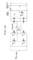
- Fig. 10 shows a circuit configuration disclosed in Patent Literature 1.
- This DC-DC converter includes a primary circuit for converting an alternate current from a direct current, a transformer, a secondary circuit for converting the alternate current into a direct current, and a smoothing filter, and feeds a DC power to a DC load.
- This DC-DC converter includes a series circuit of a resonant capacitor and a switching element (referred to as a resonant switch hereinafter) between the output terminals of the secondary circuit in order to reduce a switching loss generated in the primary circuit.
- a resonant circuit is formed by the resonant capacitor and a leakage inductor on the secondary winding side of the transformer, and by turning on the resonant switch ahead of the turnoffs of main switching elements of the primary circuit, by reducing the secondary current of the transformer that should be cut off by the main switching elements to zero using a charge-discharge current of the resonant capacitor, and by reducing the primary current of the transformer to only the level of the exciting current of the transformer, a pseudo zero current cutoff (referred to as a zero current cutoff hereinafter) is realized, with the result that the turnoff loss on the primary circuit side can be greatly reduced.
- the first problem is a problem in that, if the load coupled to the converter becomes light when the converter is continuously running, the pulse width is made small by the primary circuit so that the energy supplied by the pulse becomes small.
- the supplied energy has a lower limit. If an energy consumed by the load is smaller than the lower limit of the supplied energy, the value of the filter capacitor voltage on the output side of the DC-DC converter cannot be held constant, so that there arises a problem in that the value of the voltage across the filter capacitor becomes excessive.
- the second problem is a problem in that, when the value of the filter capacitor voltage on the output side of the DC-DC converter is low, for example, when the capacitor of the filter on the output side of the DC-DC converter is initially charged, because the voltage difference between the voltage across the secondary terminals of the transformer and the voltage across the filter capacitor on the output side and an output current flows in accordance with this voltage difference, it becomes difficult to suppress the output current, with the result that there arises a problem in that the output current becomes excessive.
- Patent Literature 2 discloses a pulse number reduction means in which the number of pulses output by a duty signal output means per unit time is reduced so that the output voltage of a smoothing circuit may become a target voltage in the case where the output voltage of the smoothing circuit is larger than the target voltage.
- Patent Literature 3 discloses another pulse number reduction means in which a predefined number of continuous pulses, that is, pulses residing in one cycle are thinning out in a lot if an output voltage exceeds a predefined reference voltage, and if the output voltage still exceeds the predefined reference voltage in spite of the above thinning-out, pulses residing in another cycle are repeatedly thinning out.
- a predefined number of continuous pulses that is, pulses residing in one cycle are thinning out in a lot if an output voltage exceeds a predefined reference voltage, and if the output voltage still exceeds the predefined reference voltage in spite of the above thinning-out, pulses residing in another cycle are repeatedly thinning out.
- Patent Literatures 2 and 3 are applied to a soft switching type DC-DC converter, on which the present invention is based, it is easy to prevent the voltage of a filter capacitor on the DC-DC converter output side from becoming excessive when a load is a light load if the filter capacitor is charged to a predefined voltage value.
- the filter capacitor voltage on the output side (particularly in the case where the initial charging of the filter capacitor is performed when the filter capacitor voltage is zero), because the charging of the capacitor is performed with the use of the resonant energy induced by a resonant circuit, particularly if the inductance of the filter reactor is relatively smaller in comparison with the capacitance of the filter capacitor, the output current rapidly increases before the filter capacitor is sufficiently charged in the pulse thinning-out operation conducted by the related arts, which leads to a problem in that the apparatus may be broken down owing to the excessive current in the worst case. In addition, if the output current becomes larger than a resonant current flowing through the resonant circuit, it becomes impossible to execute the zero current cutoff by the soft switching.
- a positive pulse voltage and a negative pulse voltage are alternately applied to the transformer; however, when the pulse thinning-out operation is performed, it is necessary to pay close attention to the polarity of the last pulse just before the start of the pulse thinning-out operation and the polarity of the first pulse just after the end of the pulse thinning-out operation.
- the transformer is magnetized in a biased manner when the stop time of pulses caused by the thinning out the pulses is short. If the biased magnetization of the transformer is intensified, the transformer gets to a magnetic saturation state, and there arises a problem in that the exciting current increases and the voltage waveform is distorted.
- a DC power supply apparatus includes, as a main circuit, a primary circuit for converting a DC power into an AC power; a transformer for bringing in the AC power output by the primary circuit; a secondary circuit for converting the AC power output by the transformer into a DC power; a resonant circuit that is coupled to the DC output side of the secondary circuit, and that includes a series circuit of a resonant switching element and a resonant capacitor; and a filter circuit for smoothing the output of the secondary circuit, and the present invention further includes, as a control circuit, a control device for supplying pulse-width modulated gate signals to main switching elements in the primary circuit and the resonant switching element and, if needed, thins out on-pulses by stopping supplying the gate signals to the main switching elements and the resonant switching element.
- This process of thinning out the on-pulses may include a means for determining the number of times of outputting on-pulses on the basis of the circuit constants of the DC-DC converter and the input power supply voltage when the voltage of the filter capacitor coupled with the output side of the secondary circuit, that is, the DC output voltage becomes larger than a DC output voltage command value by a predefined voltage, or when the DC output voltage is smaller than a predefined voltage.
- the process of thinning out the on-pulses may include a means that memorizes the polarity of the last pulse output just before the start of the thinning-out, and that stops or restarts the output of pulses in the middle of one cycle so that the polarity of the first pulse output just after the end of the thinning-out processing is opposite to the memorized polarity of the last pulse.
- the present invention can prevent an excessive current from occurring in the initial charging of the filter capacitor on the output side of the DC-DC converter by performing fine-grained thinning-out processing while preventing the biased magnetization of the transformer owing to the thinning-out operation from occurring, which enables the reliability of the DC power supply apparatus to be improved economically.
- the breakdown of the apparatus can be prevented because an excessive current in the initial charging is suppressed, and the reliability of the system can be improved.
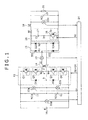
- Fig. 1 is a diagram showing a configuration example of a main circuit of a DC power supply apparatus applicable to first and second embodiments of the present invention.
- This DC power supply apparatus comprises a DC-DC converter for supplying an output DC voltage, which has a value different from the value of an input DC voltage, to a load 20 in which the output DC voltage is isolated by a combination of a primary circuit 13 that brings in the voltage of a DC voltage source 10 and converts a direct current to an alternate current, a transformer 14, and a secondary circuit 15 for converting an alternate current to a direct current.
- the primary circuit 13 is a three-level circuit including a series circuit of two filter capacitors 11 (FC11) and 12 (FC12) that is coupled in parallel to the DC voltage source 10.
- four main switching elements Q1 to Q4 are coupled in series, and a combination of series-coupled main switching elements Q1 and Q2 and a combination of series-coupled main switching elements Q3 and Q4 respectively form an upper arm and a lower arm.
- the upper arm and the lower arm are respectively coupled in parallel to the filter capacitors 11 (FC11) and 12 (FC12).
- a series circuit of clamp diodes D5 and D6 are coupled between the series-coupled point between the main switching elements in the upper arm and the main switching elements in the lower arm.
- the series-coupled point between these diodes D5 and D6 is coupled to the series-coupled point between the two filter capacitors 11 (FC11) and 12 (FC12).
- the series-coupled point "a" between the upper and lower arms and the series-coupled point “b” between the filter capacitors 11 (FC11) and 12 (FC12) make a pair of AC output terminals for an AC output, and are respectively coupled to two ends of a primary winding of the transformer 14.
- a fourth voltage sensor 22d is coupled to the DC voltage source 10 in order to detect the voltage of this DC voltage source
- a first voltage sensor 22a and a second voltage sensor 22b are respectively coupled to the filter capacitors 11 (FC11) and 12 (FC12) in order to detect the voltages across the filter capacitors 11 (FC11) and 12 (FC12).
- the transformer 14 for bringing in the AC output power of the primary circuit 13 outputs stepped-down AC power to the secondary circuit 15.
- a series circuit of a resonant switch 16 (Qz) and a resonant capacitor 17 is coupled to the DC output side of the secondary circuit 15, and when the resonant switch 16 is turned on, a resonant circuit is formed by the resonant switch 16 and a resonant reactor Lz of the inductance of the transformer 14. It will be assumed that the series circuit of the resonant switch 16 (Qz) and the resonant capacitor 17 is referred to as a resonant circuit 21 hereinafter.
- a current sensor 23 for detecting the output current of the transformer 14 is installed.
- a filter reactor 18 (Ld) and a filter capacitor 19 (FC2) are installed in order to smooth the DC power output by the secondary circuit 15, and the voltage across this filter capacitor 19 is supplied to the load 20.
- a third voltage sensor 22c is installed in order to detect the voltage across the filter capacitor 19 (FC2).
- the DC power supply apparatus includes, as a control circuit, a control device 24 that brings in the output signals of the first voltage sensor 22a to the fourth voltage sensor 22d, the output signal of the current sensor 23, and outputs gate pulse signals G1 to G4 , and Gz that are respectively supplied to the main switching elements Q1 to Q4 that comprise the primary circuit 13, and the switching element Qz that comprises the resonant switch 16.
- This DC-DC converter can temporarily reduce a secondary current I2 of the transformer 14 to zero and a primary current I1 to only the level of the exciting current of the transformer 14 by activating the resonant switch 16 to the timings of the turnoffs of the main switching elements Q1 and Q4 of the primary circuit 13, and by superimposing a resonant current Iz onto the secondary current I2 of the transformer 14.
- the turnoff loss in the primary circuit 13 can be greatly reduced.
- the primary current I1 and the secondary current I2 are zero, while the main switching elements Q1 to Q4 that comprise the primary circuit are off, back-flow currents continue to flow through diodes that comprise the secondary circuit 15.
- the main switching elements Q1 and Q2 or the main switching elements Q3 and Q4, which comprise the primary circuit 13 is turned on, the primary current I1 and the secondary current I2 begin to flow, and the magnitude of the secondary current I2 coincides with that of a load current Id.
- a current whose magnitude is equal to the magnitude of the secondary current I2 flows through one half of the diodes that comprise the secondary circuit 15 and a zero current flows through the other half of the diodes.
- Fig. 2 is a diagram showing the operation waveforms in the main circuit of the DC power supply apparatus shown in Fig. 1 . With reference to these waveforms, the normal operation of the DC power supply apparatus shown in Fig. 1 will be described.
- the main switching element Q1 is in the off-state, and the main switching element Q2 is in the on-state.
- the above state changes at the time t1, that is, the main switching element Q1 is turned on, then a current Ip flows through the main switching elements Q1 and Q2. At this time, a current Ir flows through diodes D21 and D24 of the secondary circuit 15.
- the resonant switch Qz is turned on. After that, the resonant current Iz flows owing to the resonance between the resonant reactor Lz and a resonant capacitor Cz, and the resonant capacitor Cz is charged. Owing to this resonance operation, the current Ip that flows through the main switching elements Q1 and Q2, and the current Ir that flows through the diodes D21 and D24 also increase.
- the resonant capacitor Cz is in a discharging state, and the load current Id is supplied from the resonant circuit 21, so the current Ir that flows through the diodes D21 and D24 is zero.
- the current Ip that flows through the main switching elements Q1 and Q2 is also reduced only to the exciting current of the transformer Tr. Therefore, by turning off the main switching element Q1 and the resonant switch Qz, soft switching can be realized.
- the main switching element Q3 is turned on. At this time, if discharging from the resonant capacitor Cz has been finished, the load current Id flows back through the diodes D21 to D24 of the secondary circuit 15.
- the main switching element Q2 is turned off. In this case, the current flowing through the main switching element Q2 is almost zero because the current is a very small current that flows back owing commutation in the normal operation of the DC-DC converter, which leads to a very small switching loss.
- the main switching element Q4 is turned on, and a current In flows through the main switching elements Q3 and Q4. In this case, a current Io flows through the diodes D22 and D23 of the secondary circuit 15.
- the resonant switch Qz is turned on. After this turn-on of the resonant switch Qz, the resonant current Iz flows owing to the resonance between the resonant reactor Lz and the resonant capacitor Cz, and the resonant capacitor Cz is charged. Owing to this resonance operation, the current In that flows through the main switching elements Q3 and Q4, and the current Io that flows through the diodes D22 and D23 also increase.
- the resonant capacitor Cz is in a discharging state.
- the load current is supplied from the resonant circuit 21, so the current Ir that flows through the diodes D22 and D23 is zero.
- the current In that flows through the main switching elements Q3 and Q4 is also reduced only to the exciting current of the transformer Tr. Therefore, by turning off the main switching element Q4 and the resonant switch Qz, a zero current cutoff can be realized, with the result that a switching loss caused by the turnoff can be made maximally small.
- the main switching element Q2 is turned on. At this time, because discharging from the resonant capacitor Cz has been finished, the load current Id flows back through the diodes D21 to D24 of the secondary circuit 15.
- the main switching element Q3 is turned off. In this case, the current flowing through the main switching element Q3 is almost zero because the current is a very small current that flows back owing commutation in the normal operation of the DC-DC converter, which leads to a very small switching loss.
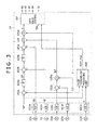
- Fig. 3 is a functional block diagram of a control device according to the first embodiment of the present invention, and shows an concrete example of the control device 24 shown in Fig. 1 .
- the control device 24 of the DC power supply apparatus includes: a first A/D converter 101a for bringing in the output signal of the third voltage sensor 22c; a second A/D converter 101b for bringing in the output signal of the first current sensor 23; a third A/D converter 101c for bringing in the output signal of the first voltage sensor 22a; a fourth A/D converter 101d for bringing in the output signal of the second voltage sensor 22b; a fifth A/D converter 101e for bringing in the output signal of the fourth voltage sensor 22d; a first subtractor 102a for calculating a difference between a DC output voltage command Vd* and the output signal (DC output voltage) Vd of the first A/D converter 101a; a first PI controller 104a for bringing in the output signal of the first subtractor 102a and outputting a load current command I
- the above-described gate pulse control 107 outputs the gate pulse signals G1 to G4 that have pulse widths corresponding to the conduction ratio ⁇ , and outputs the gate pulse signal Gz at a predefined timing when the on-command ONc is on.
- the gate pulse control 107 turns off the gate pulse signals G1 to G4 that are sent respectively to the main switching elements Q1 to Q4, and the gate pulse signal Gz sent to the resonant switch Qz.
- the gate pulse control 107 memorizes the gate pulse signal that is last output at the timing when the pulse-off signal POFF_FLG is turned on while the on-command ONc is being on.
- the gate pulse control 107 outputs a gate pulse signal whose polarity is opposite to that of the gate pulse signal output just before the pulse-off. It will be assumed that the pulse-off is executed by outputting the gate pulse signals G1 and G2 in the on-state. Afterward, when the gate pulse signals are output in the on-state again, the gate pulse control 107 runs in such a way that the gate pulse signals G3 and G4 is output in the on-state first.
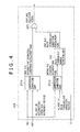
- FIG. 4 is a functional block diagram of the pulse thinning-out processing unit 108 according to the first embodiment of the present invention.
- a comparison computing unit 201a brings in the DC output voltage Vd, the DC output voltage command Vd*, and an intermittent operation reference voltage Vd_CINT_BS, and if the DC output voltage Vd is larger than the sum of the DC output voltage command Vd* and an intermittent operation reference voltage Vd_CINT_BS, the intermittent operation condition fulfillment flag CINT_FLG is output in the on-state.
- the intermittent operation condition fulfillment flag CINT_FLG is output in the off-state.
- a comparison computing unit 201b brings in the DC output voltage Vd and a pulse thinning-out operation voltage Vd_PINT_LV, and outputs a charging incompletion flag DNCHG_FLG if the DC output voltage Vd is lower than the pulse thinning-out operation voltage Vd_PINT_LV.
- a pulse thinning-out number computing unit 202 brings in the charging incompletion flag DNCHG_FLG and the voltage E of the DC voltage source, and outputs a pulse thinning-out condition fulfillment flag.
- the pulse thinning-out number computing unit 202 determines the number of pulses that can be continuously output on the basis of the voltage E of the DC voltage source when the charging incompletion flag DNCHG_FLG is on, and if the number of the output pulse becomes equal to or larger than the determined number, the pulse thinning-out number computing unit 202 outputs the pulse thinning-out condition fulfillment flag in the on-state. Afterward, the pulse thinning-out number computing unit 202 determines a time period during which pulses are continuously put in the off-state, and after a predefined time elapses, the pulse thinning-out number computing unit 202 outputs the pulse thinning-out condition fulfillment flag PINT_FLG in the off-state.
- a logical adder 203 brings in the intermittent operation condition fulfillment flag CINT_FLG and the pulse thinning-out condition fulfillment flag PINT_FLG, and outputs the result of the logical addition as a pulse-off signal POFF_FLG. Therefore, at the timing when a pulse-off condition fulfillment flag is turned on, the output of pulses by the main switching elements Q1, Q4, and by the resonant switch Qz stop, that is, the main switching elements Q1, Q4, and the resonant switch Qz remain in the off-state, with the result that a pulse thinning-out operation is performed.
- a method for configuring the number of times of outputting on-pulses and a pulse thinning-out time period in the pulse thinning-out number computing unit 202, and an operation example of the initial charging of the filter capacitor 19 will be described in detail hereinafter.
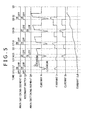
- the conduction ration ⁇ is set to the minimum conduction ratio that is limited in accordance with three quarters of the resonant cycle owing to the soft switching. Therefore, in contrast to the voltage and current waveforms of the normal operation shown in Fig. 2 , the voltage and current waveforms in this case become waveforms shown in Fig. 5 that are peculiar to a charging operation.
- This charging operation will be described with reference to Fig. 5 . Descriptions of the operations of the main switching elements Q2 and Q3 are omitted for simplicity in Fig. 5 for the sake of simplicity.
- Equation 2 the charging voltage of the resonant capacitor 17 is given by Equation 2.
- V cz 1 C z ⁇ i z ⁇ dt
- the pulse on time period ton is a time period corresponding to the minimum conduction ratio ⁇ that is limited in accordance with three quarters of the resonant cycle of the resonant circuit.
- I Lda E a 2 ⁇ n - 0 L da ⁇ t ON
- E Ldx 1 2 ⁇ L da ⁇ I Lda 2
- the current ILdb_p2 flowing through the filter reactor 18 after the second pulse is output can be obtained by adding ILda_p2, which is caused by the second pulse and given by Equation 5, to ILdb_p1, which is caused by the first pulse and given by Equation 7, by substituting the additional value of ILda_p2 and ILdb_p1 into ILda of Equation 6, by calculating the energy ELdx_p2 caused by the second pulse with the use of Equation 6, and by substituting the energy ELdx_p2 caused by the second pulse into ELdx of Equation 7.
- the current ILdb shown at the time t16 in Fig. 5 is the current flowing through the filter reactor 18 caused by the second pulse. For the third pulse and the pulses that follow, the above calculation is repeated, and the current ILdb that flows through the filter reactor 18 corresponding to the number of times of outputting on-pulses can be obtained.
- the resonant cycle of the filter reactor 18 and the filter capacitor 19 is sufficiently larger compared with that of the resonant reactor Lz and the resonant capacitor 17 (that is, the inductance of the filter reactor 18 and the capacity of the filter capacitor 19 are sufficiently larger compared with the inductance of the resonant reactor Lz and the capacity of the resonance capacitor respectively), and the capacity of the filter capacitor 19 is large. Because the capacity of the filter capacitor 19 is very large, the filter capacitor 19 is not quickly charged as shown in Fig. 6 . The voltage Vd across the filter capacitor 19 therefore does not increase quickly.
- the charging current shown by Equation 7, that is, ILd shown in Fig. 6 is incremented every time the switching is performed (every time an on-pulse is output), that is, ILd is incremented in accordance with the resonant operation. Therefore, there is a problem in that the current ILd flowing through the filter reactor 18 increases rapidly to be excessive in the initial charging when the voltage of the filter capacitor 19 is increased from zero.
- the number of times of continuously outputting on-pulses can be made larger than that of the case where the voltage Ea of the DC voltage source is equal to the rated voltage.
- the maximum number of times of continuously outputting on-pulses to limit the current flowing thorough the filter reactor 18 varies on the basis of the voltage of the DC voltage source, it is advantageous to make the number of times of outputting on-pulses configurable on the basis of the DC voltage E when the DC voltage source varies in a wide range.
- the DC output voltage command Vd* is set to be launched with a predefined variation from a target value, and after a predefined number of pulses are output with the use of the pulse thinning-out operation, the current flowing through the filter reactor 18 decreases and at the same time the charging voltage across the filter capacitor 19 gradually increases. Owing to these phenomena, the intermittent operation condition fulfillment flag CINT_FLG is output in the on-state during the time period of pulse-off, so that the pulse-off state continues. It is necessary that the time period of pulse-off set by the pulse thinning-out number computing unit 202 should last until the time when the current flowing through the filter reactor 18 decreases to some extent and the voltage across the filter capacitor 19 increases to some extent during the pulse-off.
- the gradient of the current flowing through the filter reactor 18 is equal to the output voltage across the filter reactor/the inductance of the filter reactor 18.
- the pulse thinning-out number computing unit 202 should secure a time period until the current flowing through the filter reactor 18 decrease to zero as the time period of pulse-off.
- the pulse thinning-out condition fulfillment flag PINT_FLG that is the output of the pulse thinning-out number computing unit 202 is turned off, and afterward the DC output voltage command Vd* increases, and the intermittent operation condition fulfillment flag CINT_FLG is output in the on-state, which makes the output of pulses is restarted and the charging operation continues.
- the voltage across the filter capacitor 19 has risen to a certain voltage value.
- the gate pulse control 107 configures this pulse thinning-out operation so that the polarity of the last pulse just before the start of the pulse thinning-out operation and the polarity of the first pulse when the output of pulses is restarted just after the end of the pulse thinning-out operation are opposite to each other as shown at the times t14, t15, t21, and t22, with the result that the biased magnetization of the transformer 14 can be prevented from occurring.
- the current flowing through the filter reactor can be suppressed not to be an excessive current, and at the same time the biased magnetization of the transformer can be prevented from occurring.
- This configuration does not need a voltage sensor for detecting the current flowing through the filter reactor 18 in comparison with the configuration in which an excessive current is suppressed by thinning-out pulses when the current flowing through the filter reactor 18 becomes equal to or larger than a predefined value through the detection of the current. Therefore the cost of the DC power supply apparatus can be reduced, and the credibility of the apparatus can be economically improved.
- Fig. 9 is a functional block diagram of a pulse thinning-out processing unit 108 according to the second embodiment of the present invention.
- a different point from Fig. 4 resides in the fact that the DC output voltage Vd is input into the pulse thinning-out number computing unit 202.
- the DC output voltage Vd is used in such a way that the switching from the on-state to off-state of the output of the pulse thinning-out condition fulfillment flag PINT_FLG in the pulse thinning-out number computing unit 202 is performed not after the predefined time period elapses, but it is performed on the basis of the DC output voltage Vd.
- the voltage value to which the charging voltage will reach is estimated on the basis of the number of times of outputting on-pulses in the pulse thinning-out number computing unit 202 and the DC output voltage Vd at the time when the first on-pulse is output.
- PINT_FLG the switching from the on-state to off-state of the output of the pulse thinning-out condition fulfillment flag PINT_FLG is performed, so that the charging operation continues. Because the current flowing through the filter reactor 18 has been small at the time point when the charging voltage almost reaches the estimated voltage value, the output of pulses is restarted and the charging operation is continued again at this time point.
- the estimated voltage is a voltage that the DC output voltage Vd reaches after the DC output voltage Vd is increased almost by a charging voltage ⁇ Vc that is induced by energy of the current ILdb calculated by Equation 7 with the use of the number of times of outputting on-pulses.
Landscapes
- Engineering & Computer Science (AREA)
- Power Engineering (AREA)
- Dc-Dc Converters (AREA)
- Inverter Devices (AREA)
Applications Claiming Priority (1)
| Application Number | Priority Date | Filing Date | Title |
|---|---|---|---|
| JP2012222639A JP6018870B2 (ja) | 2012-10-05 | 2012-10-05 | 直流電源装置およびその制御方法 |
Publications (3)
| Publication Number | Publication Date |
|---|---|
| EP2717451A2 true EP2717451A2 (de) | 2014-04-09 |
| EP2717451A3 EP2717451A3 (de) | 2016-11-23 |
| EP2717451B1 EP2717451B1 (de) | 2019-03-06 |
Family
ID=49165522
Family Applications (1)
| Application Number | Title | Priority Date | Filing Date |
|---|---|---|---|
| EP13183083.8A Not-in-force EP2717451B1 (de) | 2012-10-05 | 2013-09-05 | Resonante Gleichstromversorgungsvorrichtung und Steuerverfahren dafür |
Country Status (3)
| Country | Link |
|---|---|
| EP (1) | EP2717451B1 (de) |
| JP (1) | JP6018870B2 (de) |
| CN (1) | CN103715896B (de) |
Cited By (2)
| Publication number | Priority date | Publication date | Assignee | Title |
|---|---|---|---|---|
| CN111361416A (zh) * | 2018-12-26 | 2020-07-03 | 中车唐山机车车辆有限公司 | 列车中压供电系统的控制方法,控制装置及列车 |
| US12057779B2 (en) | 2019-06-19 | 2024-08-06 | Robert Bosch Gmbh | Circuit apparatus and method for controlling a secondary side of a direct voltage converter |
Families Citing this family (9)
| Publication number | Priority date | Publication date | Assignee | Title |
|---|---|---|---|---|
| JP6424733B2 (ja) * | 2015-05-15 | 2018-11-21 | 株式会社デンソー | 電力変換器制御装置 |
| KR101884686B1 (ko) | 2016-05-23 | 2018-08-30 | 숭실대학교산학협력단 | 능동 클램프 풀브릿지 컨버터 및 그 구동방법 |
| WO2017204426A1 (ko) * | 2016-05-23 | 2017-11-30 | 숭실대학교산학협력단 | 능동 클램프 풀브릿지 컨버터 및 그 구동방법 |
| KR101961412B1 (ko) * | 2017-03-15 | 2019-03-22 | 전북대학교산학협력단 | 3레벨 양방향 직류-직류 컨버터 |
| CN106849724A (zh) * | 2017-04-17 | 2017-06-13 | 中车青岛四方车辆研究所有限公司 | 辅助逆变电源 |
| CN107612409B (zh) * | 2017-09-27 | 2020-04-21 | 西安理工大学 | 带偏磁控制的精简矩阵变换器模型预测控制方法 |
| KR102105405B1 (ko) | 2018-03-21 | 2020-04-28 | 엘에스일렉트릭(주) | 고압 인버터 초기충전 시스템 및 그 제어방법 |
| CN110133351B (zh) * | 2019-04-30 | 2021-03-05 | 国网经济技术研究院有限公司 | 一种双输出光学电流互感器及其信号处理方法 |
| JP7599894B2 (ja) * | 2020-10-13 | 2024-12-16 | 株式会社東芝 | 電力変換装置 |
Citations (3)
| Publication number | Priority date | Publication date | Assignee | Title |
|---|---|---|---|---|
| JPH04368464A (ja) | 1991-06-12 | 1992-12-21 | Sanyo Denki Co Ltd | 直流電源装置 |
| JP2004159473A (ja) | 2002-11-08 | 2004-06-03 | Toyota Industries Corp | 絶縁型電圧変換回路 |
| JP2009296763A (ja) | 2008-06-04 | 2009-12-17 | Denso Corp | スイッチング電源装置 |
Family Cites Families (11)
| Publication number | Priority date | Publication date | Assignee | Title |
|---|---|---|---|---|
| JPH06237577A (ja) * | 1993-02-10 | 1994-08-23 | Meidensha Corp | コンデンサ充電電源装置 |
| US6349044B1 (en) * | 1999-09-09 | 2002-02-19 | Virginia Tech Intellectual Properties, Inc. | Zero voltage zero current three level dc-dc converter |
| JP2001275351A (ja) * | 2000-03-24 | 2001-10-05 | Sony Corp | スイッチング電源回路 |
| JP2002095249A (ja) * | 2000-09-08 | 2002-03-29 | Sanken Electric Co Ltd | スイッチング電源装置 |
| CN100405723C (zh) * | 2006-12-08 | 2008-07-23 | 南京航空航天大学 | 零电压开关pwm组合型三电平直流变换器 |
| WO2009011374A1 (ja) * | 2007-07-18 | 2009-01-22 | Murata Manufacturing Co., Ltd. | 絶縁型dc-dcコンバータ |
| CN102428639B (zh) * | 2009-04-09 | 2015-04-15 | 意法半导体股份有限公司 | 在谐振转换器中防止硬开关的方法和电路 |
| ITGE20090096A1 (it) * | 2009-12-10 | 2011-06-11 | Rgm Spa | Circuito di alimentazione in continua |
| JP5564400B2 (ja) * | 2010-03-11 | 2014-07-30 | 株式会社日立製作所 | 直流電源装置,電力変換装置 |
| JP5314724B2 (ja) * | 2011-03-03 | 2013-10-16 | 株式会社日立製作所 | 直流電源装置 |
| CN102281006A (zh) * | 2011-03-31 | 2011-12-14 | 东北大学 | 一种新型三电平软开关变换器 |
-
2012
- 2012-10-05 JP JP2012222639A patent/JP6018870B2/ja not_active Expired - Fee Related
-
2013
- 2013-09-05 EP EP13183083.8A patent/EP2717451B1/de not_active Not-in-force
- 2013-09-30 CN CN201310459811.3A patent/CN103715896B/zh not_active Expired - Fee Related
Patent Citations (3)
| Publication number | Priority date | Publication date | Assignee | Title |
|---|---|---|---|---|
| JPH04368464A (ja) | 1991-06-12 | 1992-12-21 | Sanyo Denki Co Ltd | 直流電源装置 |
| JP2004159473A (ja) | 2002-11-08 | 2004-06-03 | Toyota Industries Corp | 絶縁型電圧変換回路 |
| JP2009296763A (ja) | 2008-06-04 | 2009-12-17 | Denso Corp | スイッチング電源装置 |
Cited By (2)
| Publication number | Priority date | Publication date | Assignee | Title |
|---|---|---|---|---|
| CN111361416A (zh) * | 2018-12-26 | 2020-07-03 | 中车唐山机车车辆有限公司 | 列车中压供电系统的控制方法,控制装置及列车 |
| US12057779B2 (en) | 2019-06-19 | 2024-08-06 | Robert Bosch Gmbh | Circuit apparatus and method for controlling a secondary side of a direct voltage converter |
Also Published As
| Publication number | Publication date |
|---|---|
| EP2717451A3 (de) | 2016-11-23 |
| JP6018870B2 (ja) | 2016-11-02 |
| EP2717451B1 (de) | 2019-03-06 |
| CN103715896A (zh) | 2014-04-09 |
| CN103715896B (zh) | 2016-02-03 |
| JP2014075928A (ja) | 2014-04-24 |
Similar Documents
| Publication | Publication Date | Title |
|---|---|---|
| EP2717451B1 (de) | Resonante Gleichstromversorgungsvorrichtung und Steuerverfahren dafür | |
| CA3044742C (en) | Synchronous rectification of llc converters based on homopolarity | |
| US10374516B2 (en) | Non zero-voltage switching (ZVS) detection in resonant converters | |
| US8964414B2 (en) | DC power supply including resonant circuit for reducing switching losses | |
| US9374011B2 (en) | Secondary controller for use in synchronous flyback converter | |
| EP3522350B1 (de) | Leistungswandlervorrichtung | |
| US20180294731A1 (en) | Control device and control method | |
| US9487098B2 (en) | Power conversion apparatus | |
| US9871455B2 (en) | Current resonance type power supply device | |
| WO2013114758A1 (ja) | 共振形dc-dcコンバータの制御装置 | |
| EP2814165B1 (de) | Gleichstromversorgung | |
| US8787055B2 (en) | Inverter device | |
| US12355273B2 (en) | Power receiving device and contactless power transmission system | |
| JP4110477B2 (ja) | Dc−dcコンバータ | |
| JP7206452B2 (ja) | 電力変換装置及び電力変換装置の制御方法 | |
| US11563368B2 (en) | Power conversion device | |
| JP5797142B2 (ja) | 直流電源装置およびその制御方法 | |
| US12368368B2 (en) | Isolated resonant conversion control method, apparatus and system, and readable storage medium based on switching frequency of input-side switch transistor | |
| JP6623994B2 (ja) | 電力変換装置及び送電機器 | |
| EP4274076A1 (de) | Nullspannungsschaltung | |
| WO2014097677A1 (ja) | 双方向dc-dc変換装置及び変換装置 | |
| EP3852260A1 (de) | Leistungswandler und steuerungsverfahren für einen leistungswandler | |
| JP4398122B2 (ja) | 同期整流システムと整流方法 | |
| JPH04285476A (ja) | 電力変換装置 | |
| KR20180047479A (ko) | Dc-dc 컨버터 및 이의 구동 방법 |
Legal Events
| Date | Code | Title | Description |
|---|---|---|---|
| PUAI | Public reference made under article 153(3) epc to a published international application that has entered the european phase |
Free format text: ORIGINAL CODE: 0009012 |
|
| 17P | Request for examination filed |
Effective date: 20130918 |
|
| AK | Designated contracting states |
Kind code of ref document: A2 Designated state(s): AL AT BE BG CH CY CZ DE DK EE ES FI FR GB GR HR HU IE IS IT LI LT LU LV MC MK MT NL NO PL PT RO RS SE SI SK SM TR |
|
| AX | Request for extension of the european patent |
Extension state: BA ME |
|
| PUAL | Search report despatched |
Free format text: ORIGINAL CODE: 0009013 |
|
| AK | Designated contracting states |
Kind code of ref document: A3 Designated state(s): AL AT BE BG CH CY CZ DE DK EE ES FI FR GB GR HR HU IE IS IT LI LT LU LV MC MK MT NL NO PL PT RO RS SE SI SK SM TR |
|
| AX | Request for extension of the european patent |
Extension state: BA ME |
|
| RIC1 | Information provided on ipc code assigned before grant |
Ipc: H02M 1/36 20070101ALI20161019BHEP Ipc: H02M 3/335 20060101AFI20161019BHEP |
|
| GRAP | Despatch of communication of intention to grant a patent |
Free format text: ORIGINAL CODE: EPIDOSNIGR1 |
|
| RIC1 | Information provided on ipc code assigned before grant |
Ipc: H02M 1/36 20070101ALI20181031BHEP Ipc: H02M 3/335 20060101AFI20181031BHEP |
|
| STAA | Information on the status of an ep patent application or granted ep patent |
Free format text: STATUS: GRANT OF PATENT IS INTENDED |
|
| INTG | Intention to grant announced |
Effective date: 20181206 |
|
| GRAS | Grant fee paid |
Free format text: ORIGINAL CODE: EPIDOSNIGR3 |
|
| GRAA | (expected) grant |
Free format text: ORIGINAL CODE: 0009210 |
|
| STAA | Information on the status of an ep patent application or granted ep patent |
Free format text: STATUS: THE PATENT HAS BEEN GRANTED |
|
| AK | Designated contracting states |
Kind code of ref document: B1 Designated state(s): AL AT BE BG CH CY CZ DE DK EE ES FI FR GB GR HR HU IE IS IT LI LT LU LV MC MK MT NL NO PL PT RO RS SE SI SK SM TR |
|
| REG | Reference to a national code |
Ref country code: GB Ref legal event code: FG4D |
|
| REG | Reference to a national code |
Ref country code: CH Ref legal event code: EP Ref country code: AT Ref legal event code: REF Ref document number: 1105895 Country of ref document: AT Kind code of ref document: T Effective date: 20190315 |
|
| REG | Reference to a national code |
Ref country code: DE Ref legal event code: R096 Ref document number: 602013051733 Country of ref document: DE |
|
| REG | Reference to a national code |
Ref country code: IE Ref legal event code: FG4D |
|
| REG | Reference to a national code |
Ref country code: NL Ref legal event code: MP Effective date: 20190306 |
|
| REG | Reference to a national code |
Ref country code: LT Ref legal event code: MG4D |
|
| PG25 | Lapsed in a contracting state [announced via postgrant information from national office to epo] |
Ref country code: FI Free format text: LAPSE BECAUSE OF FAILURE TO SUBMIT A TRANSLATION OF THE DESCRIPTION OR TO PAY THE FEE WITHIN THE PRESCRIBED TIME-LIMIT Effective date: 20190306 Ref country code: SE Free format text: LAPSE BECAUSE OF FAILURE TO SUBMIT A TRANSLATION OF THE DESCRIPTION OR TO PAY THE FEE WITHIN THE PRESCRIBED TIME-LIMIT Effective date: 20190306 Ref country code: NO Free format text: LAPSE BECAUSE OF FAILURE TO SUBMIT A TRANSLATION OF THE DESCRIPTION OR TO PAY THE FEE WITHIN THE PRESCRIBED TIME-LIMIT Effective date: 20190606 Ref country code: LT Free format text: LAPSE BECAUSE OF FAILURE TO SUBMIT A TRANSLATION OF THE DESCRIPTION OR TO PAY THE FEE WITHIN THE PRESCRIBED TIME-LIMIT Effective date: 20190306 |
|
| PG25 | Lapsed in a contracting state [announced via postgrant information from national office to epo] |
Ref country code: NL Free format text: LAPSE BECAUSE OF FAILURE TO SUBMIT A TRANSLATION OF THE DESCRIPTION OR TO PAY THE FEE WITHIN THE PRESCRIBED TIME-LIMIT Effective date: 20190306 Ref country code: HR Free format text: LAPSE BECAUSE OF FAILURE TO SUBMIT A TRANSLATION OF THE DESCRIPTION OR TO PAY THE FEE WITHIN THE PRESCRIBED TIME-LIMIT Effective date: 20190306 Ref country code: RS Free format text: LAPSE BECAUSE OF FAILURE TO SUBMIT A TRANSLATION OF THE DESCRIPTION OR TO PAY THE FEE WITHIN THE PRESCRIBED TIME-LIMIT Effective date: 20190306 Ref country code: BG Free format text: LAPSE BECAUSE OF FAILURE TO SUBMIT A TRANSLATION OF THE DESCRIPTION OR TO PAY THE FEE WITHIN THE PRESCRIBED TIME-LIMIT Effective date: 20190606 Ref country code: GR Free format text: LAPSE BECAUSE OF FAILURE TO SUBMIT A TRANSLATION OF THE DESCRIPTION OR TO PAY THE FEE WITHIN THE PRESCRIBED TIME-LIMIT Effective date: 20190607 Ref country code: LV Free format text: LAPSE BECAUSE OF FAILURE TO SUBMIT A TRANSLATION OF THE DESCRIPTION OR TO PAY THE FEE WITHIN THE PRESCRIBED TIME-LIMIT Effective date: 20190306 |
|
| REG | Reference to a national code |
Ref country code: AT Ref legal event code: MK05 Ref document number: 1105895 Country of ref document: AT Kind code of ref document: T Effective date: 20190306 |
|
| PG25 | Lapsed in a contracting state [announced via postgrant information from national office to epo] |
Ref country code: EE Free format text: LAPSE BECAUSE OF FAILURE TO SUBMIT A TRANSLATION OF THE DESCRIPTION OR TO PAY THE FEE WITHIN THE PRESCRIBED TIME-LIMIT Effective date: 20190306 Ref country code: PT Free format text: LAPSE BECAUSE OF FAILURE TO SUBMIT A TRANSLATION OF THE DESCRIPTION OR TO PAY THE FEE WITHIN THE PRESCRIBED TIME-LIMIT Effective date: 20190706 Ref country code: AL Free format text: LAPSE BECAUSE OF FAILURE TO SUBMIT A TRANSLATION OF THE DESCRIPTION OR TO PAY THE FEE WITHIN THE PRESCRIBED TIME-LIMIT Effective date: 20190306 Ref country code: IT Free format text: LAPSE BECAUSE OF FAILURE TO SUBMIT A TRANSLATION OF THE DESCRIPTION OR TO PAY THE FEE WITHIN THE PRESCRIBED TIME-LIMIT Effective date: 20190306 Ref country code: CZ Free format text: LAPSE BECAUSE OF FAILURE TO SUBMIT A TRANSLATION OF THE DESCRIPTION OR TO PAY THE FEE WITHIN THE PRESCRIBED TIME-LIMIT Effective date: 20190306 Ref country code: RO Free format text: LAPSE BECAUSE OF FAILURE TO SUBMIT A TRANSLATION OF THE DESCRIPTION OR TO PAY THE FEE WITHIN THE PRESCRIBED TIME-LIMIT Effective date: 20190306 Ref country code: SK Free format text: LAPSE BECAUSE OF FAILURE TO SUBMIT A TRANSLATION OF THE DESCRIPTION OR TO PAY THE FEE WITHIN THE PRESCRIBED TIME-LIMIT Effective date: 20190306 Ref country code: ES Free format text: LAPSE BECAUSE OF FAILURE TO SUBMIT A TRANSLATION OF THE DESCRIPTION OR TO PAY THE FEE WITHIN THE PRESCRIBED TIME-LIMIT Effective date: 20190306 |
|
| PG25 | Lapsed in a contracting state [announced via postgrant information from national office to epo] |
Ref country code: SM Free format text: LAPSE BECAUSE OF FAILURE TO SUBMIT A TRANSLATION OF THE DESCRIPTION OR TO PAY THE FEE WITHIN THE PRESCRIBED TIME-LIMIT Effective date: 20190306 Ref country code: PL Free format text: LAPSE BECAUSE OF FAILURE TO SUBMIT A TRANSLATION OF THE DESCRIPTION OR TO PAY THE FEE WITHIN THE PRESCRIBED TIME-LIMIT Effective date: 20190306 |
|
| REG | Reference to a national code |
Ref country code: DE Ref legal event code: R097 Ref document number: 602013051733 Country of ref document: DE |
|
| PG25 | Lapsed in a contracting state [announced via postgrant information from national office to epo] |
Ref country code: AT Free format text: LAPSE BECAUSE OF FAILURE TO SUBMIT A TRANSLATION OF THE DESCRIPTION OR TO PAY THE FEE WITHIN THE PRESCRIBED TIME-LIMIT Effective date: 20190306 Ref country code: IS Free format text: LAPSE BECAUSE OF FAILURE TO SUBMIT A TRANSLATION OF THE DESCRIPTION OR TO PAY THE FEE WITHIN THE PRESCRIBED TIME-LIMIT Effective date: 20190706 |
|
| PLBE | No opposition filed within time limit |
Free format text: ORIGINAL CODE: 0009261 |
|
| STAA | Information on the status of an ep patent application or granted ep patent |
Free format text: STATUS: NO OPPOSITION FILED WITHIN TIME LIMIT |
|
| PG25 | Lapsed in a contracting state [announced via postgrant information from national office to epo] |
Ref country code: DK Free format text: LAPSE BECAUSE OF FAILURE TO SUBMIT A TRANSLATION OF THE DESCRIPTION OR TO PAY THE FEE WITHIN THE PRESCRIBED TIME-LIMIT Effective date: 20190306 |
|
| 26N | No opposition filed |
Effective date: 20191209 |
|
| PG25 | Lapsed in a contracting state [announced via postgrant information from national office to epo] |
Ref country code: SI Free format text: LAPSE BECAUSE OF FAILURE TO SUBMIT A TRANSLATION OF THE DESCRIPTION OR TO PAY THE FEE WITHIN THE PRESCRIBED TIME-LIMIT Effective date: 20190306 |
|
| PG25 | Lapsed in a contracting state [announced via postgrant information from national office to epo] |
Ref country code: TR Free format text: LAPSE BECAUSE OF FAILURE TO SUBMIT A TRANSLATION OF THE DESCRIPTION OR TO PAY THE FEE WITHIN THE PRESCRIBED TIME-LIMIT Effective date: 20190306 |
|
| PG25 | Lapsed in a contracting state [announced via postgrant information from national office to epo] |
Ref country code: MC Free format text: LAPSE BECAUSE OF FAILURE TO SUBMIT A TRANSLATION OF THE DESCRIPTION OR TO PAY THE FEE WITHIN THE PRESCRIBED TIME-LIMIT Effective date: 20190306 |
|
| REG | Reference to a national code |
Ref country code: CH Ref legal event code: PL |
|
| PG25 | Lapsed in a contracting state [announced via postgrant information from national office to epo] |
Ref country code: CH Free format text: LAPSE BECAUSE OF NON-PAYMENT OF DUE FEES Effective date: 20190930 Ref country code: LI Free format text: LAPSE BECAUSE OF NON-PAYMENT OF DUE FEES Effective date: 20190930 Ref country code: IE Free format text: LAPSE BECAUSE OF NON-PAYMENT OF DUE FEES Effective date: 20190905 Ref country code: LU Free format text: LAPSE BECAUSE OF NON-PAYMENT OF DUE FEES Effective date: 20190905 |
|
| REG | Reference to a national code |
Ref country code: BE Ref legal event code: MM Effective date: 20190930 |
|
| PG25 | Lapsed in a contracting state [announced via postgrant information from national office to epo] |
Ref country code: BE Free format text: LAPSE BECAUSE OF NON-PAYMENT OF DUE FEES Effective date: 20190930 |
|
| PG25 | Lapsed in a contracting state [announced via postgrant information from national office to epo] |
Ref country code: FR Free format text: LAPSE BECAUSE OF NON-PAYMENT OF DUE FEES Effective date: 20190930 |
|
| PG25 | Lapsed in a contracting state [announced via postgrant information from national office to epo] |
Ref country code: CY Free format text: LAPSE BECAUSE OF FAILURE TO SUBMIT A TRANSLATION OF THE DESCRIPTION OR TO PAY THE FEE WITHIN THE PRESCRIBED TIME-LIMIT Effective date: 20190306 |
|
| PG25 | Lapsed in a contracting state [announced via postgrant information from national office to epo] |
Ref country code: MT Free format text: LAPSE BECAUSE OF FAILURE TO SUBMIT A TRANSLATION OF THE DESCRIPTION OR TO PAY THE FEE WITHIN THE PRESCRIBED TIME-LIMIT Effective date: 20190306 Ref country code: HU Free format text: LAPSE BECAUSE OF FAILURE TO SUBMIT A TRANSLATION OF THE DESCRIPTION OR TO PAY THE FEE WITHIN THE PRESCRIBED TIME-LIMIT; INVALID AB INITIO Effective date: 20130905 |
|
| PG25 | Lapsed in a contracting state [announced via postgrant information from national office to epo] |
Ref country code: MK Free format text: LAPSE BECAUSE OF FAILURE TO SUBMIT A TRANSLATION OF THE DESCRIPTION OR TO PAY THE FEE WITHIN THE PRESCRIBED TIME-LIMIT Effective date: 20190306 |
|
| PGFP | Annual fee paid to national office [announced via postgrant information from national office to epo] |
Ref country code: GB Payment date: 20220728 Year of fee payment: 10 Ref country code: DE Payment date: 20220803 Year of fee payment: 10 |
|
| REG | Reference to a national code |
Ref country code: DE Ref legal event code: R119 Ref document number: 602013051733 Country of ref document: DE |
|
| GBPC | Gb: european patent ceased through non-payment of renewal fee |
Effective date: 20230905 |
|
| PG25 | Lapsed in a contracting state [announced via postgrant information from national office to epo] |
Ref country code: GB Free format text: LAPSE BECAUSE OF NON-PAYMENT OF DUE FEES Effective date: 20230905 |
|
| PG25 | Lapsed in a contracting state [announced via postgrant information from national office to epo] |
Ref country code: GB Free format text: LAPSE BECAUSE OF NON-PAYMENT OF DUE FEES Effective date: 20230905 Ref country code: DE Free format text: LAPSE BECAUSE OF NON-PAYMENT OF DUE FEES Effective date: 20240403 |