EP2729819B1 - Capteur de courant - Google Patents
Capteur de courant Download PDFInfo
- Publication number
- EP2729819B1 EP2729819B1 EP12751602.9A EP12751602A EP2729819B1 EP 2729819 B1 EP2729819 B1 EP 2729819B1 EP 12751602 A EP12751602 A EP 12751602A EP 2729819 B1 EP2729819 B1 EP 2729819B1
- Authority
- EP
- European Patent Office
- Prior art keywords
- thin film
- magnetic thin
- bus bar
- current sensor
- base
- Prior art date
- Legal status (The legal status is an assumption and is not a legal conclusion. Google has not performed a legal analysis and makes no representation as to the accuracy of the status listed.)
- Not-in-force
Links
Images


Classifications
-
- G—PHYSICS
- G01—MEASURING; TESTING
- G01R—MEASURING ELECTRIC VARIABLES; MEASURING MAGNETIC VARIABLES
- G01R19/00—Arrangements for measuring currents or voltages or for indicating presence or sign thereof
- G01R19/0092—Measuring current only
-
- G—PHYSICS
- G01—MEASURING; TESTING
- G01R—MEASURING ELECTRIC VARIABLES; MEASURING MAGNETIC VARIABLES
- G01R15/00—Details of measuring arrangements of the types provided for in groups G01R17/00 - G01R29/00, G01R33/00 - G01R33/26 or G01R35/00
- G01R15/14—Adaptations providing voltage or current isolation, e.g. for high-voltage or high-current networks
- G01R15/24—Adaptations providing voltage or current isolation, e.g. for high-voltage or high-current networks using light-modulating devices
- G01R15/245—Adaptations providing voltage or current isolation, e.g. for high-voltage or high-current networks using light-modulating devices using magneto-optical modulators, e.g. based on the Faraday or Cotton-Mouton effect
- G01R15/246—Adaptations providing voltage or current isolation, e.g. for high-voltage or high-current networks using light-modulating devices using magneto-optical modulators, e.g. based on the Faraday or Cotton-Mouton effect based on the Faraday, i.e. linear magneto-optic, effect
-
- G—PHYSICS
- G01—MEASURING; TESTING
- G01R—MEASURING ELECTRIC VARIABLES; MEASURING MAGNETIC VARIABLES
- G01R19/00—Arrangements for measuring currents or voltages or for indicating presence or sign thereof
- G01R19/145—Indicating the presence of current or voltage
- G01R19/15—Indicating the presence of current
-
- G—PHYSICS
- G01—MEASURING; TESTING
- G01R—MEASURING ELECTRIC VARIABLES; MEASURING MAGNETIC VARIABLES
- G01R33/00—Arrangements or instruments for measuring magnetic variables
- G01R33/02—Measuring direction or magnitude of magnetic fields or magnetic flux
- G01R33/032—Measuring direction or magnitude of magnetic fields or magnetic flux using magneto-optic devices, e.g. Faraday or Cotton-Mouton effect
- G01R33/0322—Measuring direction or magnitude of magnetic fields or magnetic flux using magneto-optic devices, e.g. Faraday or Cotton-Mouton effect using the Faraday or Voigt effect
-
- H—ELECTRICITY
- H02—GENERATION; CONVERSION OR DISTRIBUTION OF ELECTRIC POWER
- H02M—APPARATUS FOR CONVERSION BETWEEN AC AND AC, BETWEEN AC AND DC, OR BETWEEN DC AND DC, AND FOR USE WITH MAINS OR SIMILAR POWER SUPPLY SYSTEMS; CONVERSION OF DC OR AC INPUT POWER INTO SURGE OUTPUT POWER; CONTROL OR REGULATION THEREOF
- H02M1/00—Details of apparatus for conversion
- H02M1/0003—Details of control, feedback or regulation circuits
- H02M1/0009—Devices or circuits for detecting current in a converter
Definitions
- the invention relates to a current sensor and, more particularly, to a current sensor that detects a current through light with the use of a magnetic thin film.
- a current measuring device As for a current measuring device using light, there is suggested a current measuring device (for example, see Japanese Patent Application Publication No. 7-174790 ( JP 7-174790 A )).
- a current measuring device light emitted from a light source is converted by a polarizer into linearly polarized light, the polarization direction of the linearly polarized light is rotated by a magneto-optical element owing to the magneto-optical effect, the linearly polarized light having any polarization direction is split by an analyzer into two orthogonal polarization components and then emitted in different directions, and then the intensities of light beams, split into two polarization components, are respectively separately converted by two photoreceptors into electric signals.
- US 5 663 652 discloses an apparatus and method for measuring the current distribution in an integrated circuit with high time resolution.
- the apparatus incorporates a magneto-optic film, a linearly polarized light beam and a means for measuring the magneto-optic polarization rotation of a light beam and circuitry for synchronizing test pulses in an integrated circuit.
- the invention provides a current sensor that suppresses variations in the characteristic of the sensor to make it possible to improve the accuracy of detecting a current.
- the invention provides a current sensor as defined in claim 1, or any one of the dependent claims.
- An aspect of the invention relates to a current sensor for detecting a current that flows through a bus bar.
- the current sensor includes: a base that is attached to the bus bar; a magnetic thin film that is mounted on the base; a luminescent device that irradiates light to the magnetic thin film; a photoreceptor device that detects light that is irradiated from the luminescent device to the magnetic thin film and that is reflected from the magnetic thin film; a computing device that converts an optical signal, detected by the photoreceptor device, into the current that flows through the bus bar; and a rotation restricting portion that restricts relative rotation of the magnetic thin film with respect to the bus bar.
- the rotation restricting portion includes a mounting position restricting portion that restricts a mounting position of the magnetic thin film on the base and a base fixing portion that restricts relative rotation of the base with respect to the bus bar.
- the mounting position restricting portion may have a wall portion that surrounds the magnetic thin film.
- the base fixing portion may have a reference pin that protrudes from the base toward the bus bar and that is inserted in a reference hole , formed in the bus bar.
- the current sensor may further include a restricting member that restricts an angle of a passage of incident light, irradiated to the magnetic thin film, with respect to a surface of the magnetic thin film and an angle of a passage of reflected light, reflected from the magnetic thin film, with respect to the surface of the magnetic thin film.
- the current sensor is able to suppress variations in the characteristic of the sensor to thereby make it possible to improve the accuracy of detecting a current.
- FIG. 1 is a cross-sectional view that shows the configuration of a current sensor 1 according to the present embodiment.
- FIG. 2 is a plan view of the current sensor 1.
- FIG. 3 is a cross-sectional view of the current sensor 1, taken along the line III-III in FIG. 2 .
- FIG. 4 is an exploded perspective view of the current sensor 1. The configuration of the current sensor 1 according to the present embodiment will be described with reference to FIG. 1 to FIG. 4 .
- the current sensor 1 is used to detect a current that flows through a long slender rod-shaped electrically conductive bus bar 100.
- the current sensor 1 includes a magnetic thin film 20.
- the magnetic thin film 20 is made of a material having a magnetocrystalline anisotropy.
- the magnetic thin film 20 is mounted on a base 10.
- the base 10 has a planar (plate-like) body portion 12 and a pair of leg portions 16.
- the magnetic thin film 20 is mounted on the body portion 12.
- the pair of leg portions 16 protrude from one of the faces of the body portion 12.
- the body portion 12 has a planar rectangular recess 14 at the other face that is opposite to the face from which the leg portions 16 protrude.
- the recess 14 is formed such that part of the body portion 12 is recessed.
- Each of the leg portions 16 has a pawl 18 at its distal end.
- the base 10 is, for example, made of a resin material.
- the bus bar 100 has through holes 102 that extend (or penetrate) through the bus bar 100 in the thickness direction.
- the leg portions 16 are respectively inserted through the through holes 102, and the pawls 18 at the lower ends of the leg portions 16 extending through the through holes 102 are engaged with the opposite face of the bus bar 100.
- the base 10 is fixed to the bus bar 100. Note that it is not limited to the configuration that the base 10 is fixed to the bus bar 100 by the engagement of the pawls 18 with the through holes 102; for example, the base 10 may be fixedly screwed to the bus bar 100.
- the bus bar 100 has a pair of through holes 103 that serve as reference holes.
- the through holes 103 extend (or penetrate) through the bus bar 100 in the thickness direction.
- the body portion 12 of the base 10 has a pair of through holes 13 that extend (or penetrate) through the body portion 12 in the thickness direction.
- the through holes 13 and 103 are formed such that the through holes 13 and the through holes 103 respectively overlap each other in a state where the leg portions 16 of the base 10 are fitted to the through holes 102 of the bus bar 100 to place the body portion 12 on the surface of the bus bar 100.
- Pins 40 that serve as reference pins are arranged so as to extend through the through holes 13 and 103 in a state where the base 10 is assembled to the bus bar 100.
- An accommodation member 30 is fitted to the recess 14 formed in the body portion 12 of the base 10.
- the accommodation member 30 accommodates the magnetic thin film 20.
- the magnetic thin film 20 is mounted on the base 10 via the accommodation member 30.
- the accommodation member 30 has an accommodation hole that is used to accommodate the magnetic thin film 20.
- the accommodation hole is formed so that the back face of the magnetic thin film 20 contacts with the bottom face 32 of the accommodation hole and the lateral end face of the magnetic thin film 20 faces the inner wall surface 34 of the accommodation hole.
- the planar shape of the accommodation hole is also a square shape.
- the dimensions (other than the thickness) of the accommodation hole are respectively equal to the longitudinal and lateral lengths across the magnetic thin film 20 or (as long as the magnetic thin film 20 does not lose the function as a magnetic thin film) are respectively slightly smaller than the longitudinal and lateral lengths across the magnetic thin film 20 so that the magnetic thin film 20 is fitted to the accommodation hole. Therefore, a misalignment of the magnetic thin film 20, accommodated inside the accommodation hole, with respect to the accommodation member 30 is suppressed.
- the shape of the accommodation member 30 is rectangular in plan view.
- the square planar-shaped accommodation hole is formed at the center of the accommodation member 30.
- the thickness of the accommodation member 30 is gradually increased from the accommodation hole toward the edge of the accommodation member (tapered portions).
- the tapered portions function as restricting members 36.
- the restricting members 36 restrict the angle of the passage of incident light, irradiated toward the surface 22 of the magnetic thin film 20 accommodated in the accommodation hole, with respect to the surface 22 of the magnetic thin film 20, and the angle of the passage of reflected light, that the incident light is reflected from the surface 22 of the magnetic thin film 20, with respect to the surface 22 of the magnetic thin film 20.
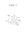
- FIG. 5 is a schematic view that shows the configuration of an optical system used in the current sensor 1. Note that FIG. 5 and FIG. 6 and FIG. 7 (described later) only show the bus bar 100 for transferring output current and the magnetic thin film 20 mounted on the bus bar 100 within the configuration of the current sensor 1, described with reference to FIG. 1 to FIG. 4 , for the sake of simplification.
- the current sensor 1 detects a current flowing through the bus bar 100 with the use of the magnetic thin film 20 fixedly attached to the bus bar 100.
- light generated by a luminescent device 50 is irradiated toward the magnetic thin film 20 via a polarizing prism 52 and a condenser lens 54.
- Reflected light reflected from the surface of the magnetic thin film 20 enters a beam splitter 58 via the condenser lens 54 and a quarter wave length plate 56, split by the beam splitter 58 into two light beams, and then the two light beams respectively enter photodiodes 61 and 62.
- the photodiodes 61 and 62 are included in a photoreceptor device 60.
- the photoreceptor device 60 detects light that is irradiated from the luminescent device 50 toward the magnetic thin film 20 and that is reflected from the magnetic thin film 20.
- the photodiodes 61 and 62 respectively detect the intensities of light beams, which respectively enter the photodiodes 61 and 62, and inputs the detected intensities to a differential amplifier 70.
- the differential amplifier 70 is a computing device that converts optical signals, respectively detected by the photodiodes 61 and 62, into a current that flows through the bus bar 100.
- the magnetic moment of the magnetic thin film 20 rotates to change the intensities of light beams that are split by the beam splitter 58 and that respectively enter the two photodiodes 61 and 62, causing a differential between the intensities of light beams that enter the photodiodes 61 and 62.
- the output appears from the differential amplifier 70.
- FIG. 6 is a schematic plan view that shows the current sensor 1 in a state where the magnetic thin film 20 is positioned.
- FIG. 7 is a schematic plan view that shows the current sensor 1 in a state where there is a misalignment of the magnetic thin film 20.
- the magnetic thin film 20 has a crystal orientation that is easy to be magnetized (axis of easy magnetization) and a crystal orientation that is hard to be magnetized (axis of hard magnetization).
- axis of easy magnetization is indicated by the alternate long and two short dashes line EMA
- axis of hard magnetization is indicated by the alternate long and two short dashes line HMA.
- the state where the magnetic thin film 20 is positioned is a state where the relative position of the magnetic thin film 20 with respect to the bus bar 100 is set such that the axis of easy magnetization EMA is aligned in the direction CD of current that flows through the bus bar 100 and the axis of hard magnetization HMA is aligned in the direction MD of the magnetic field in the magnetic thin film 20.
- the positioned state shown in FIG. 6 is an ideal state where the magnetic field generated by current flowing through the bus bar 100 is applied to the magnetic thin film 20 in the direction along the axis of hard magnetization HMA.
- the state where the magnetic thin film 20 is misaligned is a state where the magnetic thin film 20 is relatively rotated by an angle ⁇ with respect to the bus bar 100 and, as a result, the axis of easy magnetization EMA and the axis of hard magnetization HMA respectively deviate by the angle ⁇ from the direction of the current and the direction MD of the magnetic field.
- a magnetic field having a magnitude that is obtained by multiplying sin ⁇ by the magnitude of the magnetic field applied to the magnetic thin film 20 in the ideal state is applied to the magnetic thin film 20 in the direction along the axis of easy magnetization EMA.
- the magnetized direction of the magnetic thin film 20 is not aligned in one direction as compared with the ideal state, and the direction in which the magnetic field is applied to the magnetic thin film 20 varies.
- the current sensor 1 has a different characteristic.
- the sensitivity of current detection decreases, and the measuring accuracy of the current sensor 1 decreases. Therefore, in order to improve the measuring accuracy of the current sensor 1, it is important to maintain the relative position of the magnetic thin film 20 with respect to the bus bar 100 in the ideal state shown in FIG. 6 .
- the current sensor 1 includes a rotation restricting portion that is used to restrict relative rotation of the magnetic thin film 20 with respect to the bus bar 100.
- the rotation restricting portion includes a mounting position restricting portion and a base fixing portion.
- the mounting position restricting portion restricts the mounting position of the magnetic thin film 20 on the base 10.
- the base fixing portion restricts relative rotation of the base 10 with respect to the bus bar 100.
- the accommodation member 30 that accommodates the magnetic thin film 20, shown in FIG. 1 to FIG. 4 functions as the mounting position restricting portion.
- the magnetic thin film 20 is surrounded by the inner wall surface 34 of the accommodation hole.
- the inner wall surface 34 of the accommodation hole functions as a vertical wall portion that surrounds the magnetic thin film 20 accommodated inside the accommodation hole.
- the accommodation member 30 fitted in the recess 14 formed in the base 10 has the vertical wall portion that is used to fix the magnetic thin film 20. By so doing, a misalignment of the magnetic thin film 20 with respect to the base 10 is restricted.
- the pins 40 shown in FIG. 1 to FIG. 4 function as the base fixing portion.
- the two pins 40 that serve as the reference pins are arranged through the through holes 13 and the through holes 103.
- the through holes 13 are formed in the base 10.
- the through holes 103 are formed in the bus bar 100 and serve as the reference holes.
- the reference pins may have any configuration as long as the reference pins protrude from the base 10 toward the bus bar 100 and are inserted through the through holes 103, and are not limited to the example in which the pins 40 that are separate members from the base 10 and the bus bar 100 are used.
- the body portion 12 of the base 10 may partially have protrusions that are inserted through the through holes 103.
- the through holes 103 may not extend through the bus bar 100 in the thickness direction or the reference pins may be inserted in closed-end holes recessed from the surface of the bus bar 100 at the side at which the body portion 12 of the base 10 is placed.
- the magnetic thin film 20 is positioned with respect to the bus bar 100 to restrict relative rotation of the magnetic thin film 20 with respect to the bus bar 100.
- the mounting position of the magnetic thin film 20 on the bus bar 100 is restricted to form a structure that minimizes variations at the time of assembling the magnetic thin film 20 to the bus bar 100.
- a misalignment of the magnetic thin film 20 with respect to the bus bar 100 may be suppressed, and variations in the characteristic of the current sensor 1 may be suppressed.
- the current sensor 1 has the restricting member that restricts the angle of incident light to the magnetic thin film 20 and the angle of reflected light from the magnetic thin film 20.
- the incident and reflected angles of light with respect to the magnetic thin film 20 are defined as the angle made between the travelling direction of the incident light and the normal to the surface of the magnetic thin film 20 and the angle made between the travelling direction of the reflected light and the normal to the surface of the magnetic thin film 20.
- the restricting members 36 having a sufficient height with respect to the thickness of the magnetic thin film 20 are arranged around the magnetic thin film 20.
- the current sensor 1 according to the embodiment of the invention may be particularly advantageously applied to an inverter current sensor that is used to detect a current flowing through an inverter used to drive an electric motor for an electric vehicle.
Landscapes
- Physics & Mathematics (AREA)
- Engineering & Computer Science (AREA)
- Power Engineering (AREA)
- General Physics & Mathematics (AREA)
- Condensed Matter Physics & Semiconductors (AREA)
- Measuring Instrument Details And Bridges, And Automatic Balancing Devices (AREA)
Claims (5)
- Capteur de courant pour détecter un courant qui circule à travers une barre omnibus comprenant un dispositif luminescent (50) qui rayonne de la lumière sur un film magnétique fin (20),
un dispositif photorécepteur (60) qui détecte la lumière qui est rayonnée à partir du dispositif luminescent (50) jusqu'au film magnétique fin (20) et qui est réfléchie à partir du film magnétique fin (20), et
un amplificateur différentiel (70) qui convertit un signal optique, détecté par le dispositif photorécepteur (60), en un courant qui circule à travers la barre omnibus,
caractérisé en ce qu'il comprend :des trous (102) qui s'étendent à travers la barre omnibus dans le sens de l'épaisseur ;une base (10) qui est prévue avec la barre omnibus, la base (10) ayant une paire de parties de patte (16) qui ont des cliquets (18) au niveau de leur extrémité distale et les parties de patte (16) étant respectivement insérées à travers les trous débouchants (102) de sorte que les cliquets (18) se mettent en prise avec la face opposée de la barre omnibus ;le film magnétique fin (20) étant monté sur la base (10) via un élément de logement (30) servant de partie de restriction de position de montage ; etune partie de restriction de rotation qui limite la rotation relative du film magnétique fin (20) par rapport à la barre omnibus,la partie de restriction de rotation comprenant une partie de restriction de position de montage qui limite une position de montage du film magnétique fin (20) sur la base (10) et la partie de restriction de rotation comprenant une partie de fixation de base qui limite la rotation relative de la base (10) par rapport à la barre omnibus. - Capteur de courant selon la revendication 1, dans lequel
la partie de restriction de position de montage a une partie de paroi qui entoure le film magnétique fin (20). - Capteur de courant selon la revendication 1, dans lequel
la partie de restriction de position de montage a un trou de logement sur lequel le film magnétique fin (20) est monté. - Capteur de courant selon la revendication 1, 2 ou 3, dans lequel
la partie de fixation de base a une broche de référence qui fait saillie de la base (10) vers la barre omnibus et qui est insérée dans un trou de référence formé dans la barre omnibus. - Capteur de courant selon l'une quelconque des revendications 1 à 4, comprenant en outre :un élément de restriction (36) qui limite un angle d'un passage de lumière incidente, rayonnée sur le film magnétique fin (20), par rapport à une surface du film magnétique fin (20) et un angle d'un passage de lumière réfléchie, réfléchie à partir du film magnétique fin (20), par rapport à la surface du film magnétique fin (20).
Applications Claiming Priority (2)
| Application Number | Priority Date | Filing Date | Title |
|---|---|---|---|
| JP2011149012A JP2013015437A (ja) | 2011-07-05 | 2011-07-05 | 電流センサ |
| PCT/IB2012/001320 WO2013005096A1 (fr) | 2011-07-05 | 2012-07-04 | Capteur de courant |
Publications (3)
| Publication Number | Publication Date |
|---|---|
| EP2729819A1 EP2729819A1 (fr) | 2014-05-14 |
| EP2729819B1 true EP2729819B1 (fr) | 2015-08-19 |
| EP2729819B8 EP2729819B8 (fr) | 2015-09-23 |
Family
ID=46755046
Family Applications (1)
| Application Number | Title | Priority Date | Filing Date |
|---|---|---|---|
| EP12751602.9A Not-in-force EP2729819B8 (fr) | 2011-07-05 | 2012-07-04 | Capteur de courant |
Country Status (5)
| Country | Link |
|---|---|
| US (1) | US20140132247A1 (fr) |
| EP (1) | EP2729819B8 (fr) |
| JP (1) | JP2013015437A (fr) |
| CN (1) | CN103635818A (fr) |
| WO (1) | WO2013005096A1 (fr) |
Families Citing this family (5)
| Publication number | Priority date | Publication date | Assignee | Title |
|---|---|---|---|---|
| JP6581081B2 (ja) * | 2014-06-04 | 2019-09-25 | 浜松ホトニクス株式会社 | 検査装置及び磁気光学結晶の配置方法 |
| DE102015009603B4 (de) * | 2015-07-24 | 2019-05-09 | Te Connectivity Germany Gmbh | Vorrichtung zum messen eines elektrischen stromes durch eine stromschiene |
| DE102019123472B3 (de) * | 2019-09-02 | 2021-03-04 | Infineon Technologies Ag | Sensorvorrichtungen mit Sensorchip und Stromschiene |
| DE102019125537B3 (de) * | 2019-09-23 | 2021-02-18 | Infineon Technologies Ag | Sensorvorrichtungen mit Sensorchip und Stromschiene |
| CN112666377A (zh) * | 2020-12-31 | 2021-04-16 | 国网河南省电力公司南阳供电公司 | 一种开关柜三相母线电流测量装置 |
Family Cites Families (13)
| Publication number | Priority date | Publication date | Assignee | Title |
|---|---|---|---|---|
| US4612500A (en) * | 1984-09-04 | 1986-09-16 | Westinghouse Electric Corp. | Temperature stabilized Faraday rotator current sensor by thermal mechanical means |
| US4947107A (en) * | 1988-06-28 | 1990-08-07 | Sundstrand Corporation | Magneto-optic current sensor |
| US5451863A (en) * | 1992-10-30 | 1995-09-19 | International Business Machines Corporation | Fiber optic probe with a magneto-optic film on an end surface for detecting a current in an integrated circuit |
| JPH07174790A (ja) | 1993-12-20 | 1995-07-14 | Toshiba Corp | 光による電流測定装置 |
| JP3032423B2 (ja) * | 1994-04-08 | 2000-04-17 | 株式会社三協精機製作所 | 回転検出装置 |
| JPH0950613A (ja) * | 1995-08-03 | 1997-02-18 | Sony Corp | 磁気抵抗効果素子及び磁界検出装置 |
| US6211673B1 (en) * | 1997-06-03 | 2001-04-03 | International Business Machines Corporation | Apparatus for use in magnetic-field detection and generation devices |
| JP3997666B2 (ja) * | 1999-08-31 | 2007-10-24 | 株式会社デンソー | 脈波センサ |
| JP4788922B2 (ja) | 2007-05-07 | 2011-10-05 | Tdk株式会社 | 電流センサ |
| JP5403792B2 (ja) * | 2008-08-29 | 2014-01-29 | 矢崎総業株式会社 | 電流検出装置の組付け構造 |
| JP5083135B2 (ja) * | 2008-09-10 | 2012-11-28 | 株式会社デンソー | 電流センサ及び電流センサの製造方法 |
| JP5225884B2 (ja) * | 2009-02-13 | 2013-07-03 | 矢崎総業株式会社 | 電流検出装置の組付け構造及び組付け方法 |
| CN101893655B (zh) * | 2009-05-21 | 2014-02-19 | 福州大学 | 一种数字光学电流传感器 |
-
2011
- 2011-07-05 JP JP2011149012A patent/JP2013015437A/ja active Pending
-
2012
- 2012-07-04 WO PCT/IB2012/001320 patent/WO2013005096A1/fr not_active Ceased
- 2012-07-04 CN CN201280033007.2A patent/CN103635818A/zh active Pending
- 2012-07-04 EP EP12751602.9A patent/EP2729819B8/fr not_active Not-in-force
- 2012-07-04 US US14/130,582 patent/US20140132247A1/en not_active Abandoned
Also Published As
| Publication number | Publication date |
|---|---|
| US20140132247A1 (en) | 2014-05-15 |
| EP2729819B8 (fr) | 2015-09-23 |
| WO2013005096A1 (fr) | 2013-01-10 |
| JP2013015437A (ja) | 2013-01-24 |
| EP2729819A1 (fr) | 2014-05-14 |
| CN103635818A (zh) | 2014-03-12 |
Similar Documents
| Publication | Publication Date | Title |
|---|---|---|
| EP2729819B1 (fr) | Capteur de courant | |
| US10036786B2 (en) | Magnetic field measuring apparatus and manufacturing method of magnetic field measuring apparatus | |
| CN103403500B (zh) | 旋转角度检测装置 | |
| US6707292B2 (en) | Magnetic circuit for a rotary position sensor | |
| US11614472B2 (en) | Current sensor based on the Faraday effect in an atomic gas | |
| CN103162836A (zh) | 一种光偏振微小转角的光学干涉检测装置及方法 | |
| JP2001059851A (ja) | 電流検出装置及び電流検出方法 | |
| EP0501726B1 (fr) | Dispositif de mesure de champs magnétiques | |
| CN103038647B (zh) | 电流检测装置 | |
| JP2007057324A (ja) | 光ファイバ型計測システム | |
| Ghosh et al. | Observation of the Faraday effect via beam deflection in a longitudinal magnetic field | |
| KR20160086463A (ko) | 수직 광자기 컬 효과 현미경을 이용한 나노 박막에서의 수직자기 이방 자기장 측정 방법 | |
| WO2017018953A1 (fr) | Porte-échantillon multi-fonctionnel et système de détection à haute résolution destiné à des mesures d'effet kerr magnéto-optique | |
| JP4836862B2 (ja) | 光電圧センサ | |
| US20220034642A1 (en) | Rotary angle detecting device | |
| JP2770538B2 (ja) | 磁性流体磁気センサ | |
| JP3233129B2 (ja) | 磁気検出装置 | |
| JP2012229954A (ja) | 光ファイバ電流センサ | |
| CN223551177U (zh) | 一种高精度偏振度测试仪 | |
| US20250072803A1 (en) | Optically pumped magnetometer and magnetoencephalograph | |
| JP6603634B2 (ja) | 電界センサ | |
| KR20230139294A (ko) | 편광 현미경 장치 및 시야내 보정 해석 방법 | |
| CN120539642A (zh) | 基于法拉第磁致旋光效应的磁场测量装置和测量方法 | |
| JP2013253890A (ja) | 光プローブ電流センサ | |
| JPH11337370A (ja) | 磁気検出装置 |
Legal Events
| Date | Code | Title | Description |
|---|---|---|---|
| PUAI | Public reference made under article 153(3) epc to a published international application that has entered the european phase |
Free format text: ORIGINAL CODE: 0009012 |
|
| 17P | Request for examination filed |
Effective date: 20140102 |
|
| AK | Designated contracting states |
Kind code of ref document: A1 Designated state(s): AL AT BE BG CH CY CZ DE DK EE ES FI FR GB GR HR HU IE IS IT LI LT LU LV MC MK MT NL NO PL PT RO RS SE SI SK SM TR |
|
| 17Q | First examination report despatched |
Effective date: 20140515 |
|
| DAX | Request for extension of the european patent (deleted) | ||
| REG | Reference to a national code |
Ref country code: DE Ref legal event code: R079 Ref document number: 602012009833 Country of ref document: DE Free format text: PREVIOUS MAIN CLASS: G01R0015240000 Ipc: G01R0019150000 |
|
| RIC1 | Information provided on ipc code assigned before grant |
Ipc: G01R 33/032 20060101ALI20150211BHEP Ipc: G01R 19/15 20060101AFI20150211BHEP Ipc: G01R 19/00 20060101ALI20150211BHEP Ipc: G01R 15/24 20060101ALI20150211BHEP |
|
| GRAP | Despatch of communication of intention to grant a patent |
Free format text: ORIGINAL CODE: EPIDOSNIGR1 |
|
| INTG | Intention to grant announced |
Effective date: 20150324 |
|
| GRAS | Grant fee paid |
Free format text: ORIGINAL CODE: EPIDOSNIGR3 |
|
| GRAA | (expected) grant |
Free format text: ORIGINAL CODE: 0009210 |
|
| RAP1 | Party data changed (applicant data changed or rights of an application transferred) |
Owner name: TOYOTA JIDOSHA KABUSHIKI KAISHA |
|
| AK | Designated contracting states |
Kind code of ref document: B1 Designated state(s): AL AT BE BG CH CY CZ DE DK EE ES FI FR GB GR HR HU IE IS IT LI LT LU LV MC MK MT NL NO PL PT RO RS SE SI SK SM TR |
|
| RAP1 | Party data changed (applicant data changed or rights of an application transferred) |
Owner name: TOYOTA JIDOSHA KABUSHIKI KAISHA |
|
| REG | Reference to a national code |
Ref country code: GB Ref legal event code: FG4D |
|
| RIN1 | Information on inventor provided before grant (corrected) |
Inventor name: KIKUCHI, NAOTO Inventor name: SEO, YUSUKE Inventor name: TAKAGI, KENICHI |
|
| REG | Reference to a national code |
Ref country code: CH Ref legal event code: EP |
|
| REG | Reference to a national code |
Ref country code: IE Ref legal event code: FG4D |
|
| REG | Reference to a national code |
Ref country code: AT Ref legal event code: REF Ref document number: 744186 Country of ref document: AT Kind code of ref document: T Effective date: 20150915 |
|
| RIN2 | Information on inventor provided after grant (corrected) |
Inventor name: KIKUCHI, NAOTO Inventor name: SEO, YUSUKE Inventor name: TAKAGI, KENICHI |
|
| REG | Reference to a national code |
Ref country code: DE Ref legal event code: R096 Ref document number: 602012009833 Country of ref document: DE |
|
| REG | Reference to a national code |
Ref country code: AT Ref legal event code: MK05 Ref document number: 744186 Country of ref document: AT Kind code of ref document: T Effective date: 20150819 |
|
| REG | Reference to a national code |
Ref country code: LT Ref legal event code: MG4D |
|
| REG | Reference to a national code |
Ref country code: NL Ref legal event code: MP Effective date: 20150819 |
|
| PG25 | Lapsed in a contracting state [announced via postgrant information from national office to epo] |
Ref country code: FI Free format text: LAPSE BECAUSE OF FAILURE TO SUBMIT A TRANSLATION OF THE DESCRIPTION OR TO PAY THE FEE WITHIN THE PRESCRIBED TIME-LIMIT Effective date: 20150819 Ref country code: GR Free format text: LAPSE BECAUSE OF FAILURE TO SUBMIT A TRANSLATION OF THE DESCRIPTION OR TO PAY THE FEE WITHIN THE PRESCRIBED TIME-LIMIT Effective date: 20151120 Ref country code: LV Free format text: LAPSE BECAUSE OF FAILURE TO SUBMIT A TRANSLATION OF THE DESCRIPTION OR TO PAY THE FEE WITHIN THE PRESCRIBED TIME-LIMIT Effective date: 20150819 Ref country code: LT Free format text: LAPSE BECAUSE OF FAILURE TO SUBMIT A TRANSLATION OF THE DESCRIPTION OR TO PAY THE FEE WITHIN THE PRESCRIBED TIME-LIMIT Effective date: 20150819 Ref country code: NO Free format text: LAPSE BECAUSE OF FAILURE TO SUBMIT A TRANSLATION OF THE DESCRIPTION OR TO PAY THE FEE WITHIN THE PRESCRIBED TIME-LIMIT Effective date: 20151119 |
|
| PG25 | Lapsed in a contracting state [announced via postgrant information from national office to epo] |
Ref country code: SE Free format text: LAPSE BECAUSE OF FAILURE TO SUBMIT A TRANSLATION OF THE DESCRIPTION OR TO PAY THE FEE WITHIN THE PRESCRIBED TIME-LIMIT Effective date: 20150819 Ref country code: HR Free format text: LAPSE BECAUSE OF FAILURE TO SUBMIT A TRANSLATION OF THE DESCRIPTION OR TO PAY THE FEE WITHIN THE PRESCRIBED TIME-LIMIT Effective date: 20150819 Ref country code: PL Free format text: LAPSE BECAUSE OF FAILURE TO SUBMIT A TRANSLATION OF THE DESCRIPTION OR TO PAY THE FEE WITHIN THE PRESCRIBED TIME-LIMIT Effective date: 20150819 Ref country code: PT Free format text: LAPSE BECAUSE OF FAILURE TO SUBMIT A TRANSLATION OF THE DESCRIPTION OR TO PAY THE FEE WITHIN THE PRESCRIBED TIME-LIMIT Effective date: 20151221 Ref country code: IS Free format text: LAPSE BECAUSE OF FAILURE TO SUBMIT A TRANSLATION OF THE DESCRIPTION OR TO PAY THE FEE WITHIN THE PRESCRIBED TIME-LIMIT Effective date: 20151219 Ref country code: RS Free format text: LAPSE BECAUSE OF FAILURE TO SUBMIT A TRANSLATION OF THE DESCRIPTION OR TO PAY THE FEE WITHIN THE PRESCRIBED TIME-LIMIT Effective date: 20150819 Ref country code: AT Free format text: LAPSE BECAUSE OF FAILURE TO SUBMIT A TRANSLATION OF THE DESCRIPTION OR TO PAY THE FEE WITHIN THE PRESCRIBED TIME-LIMIT Effective date: 20150819 Ref country code: ES Free format text: LAPSE BECAUSE OF FAILURE TO SUBMIT A TRANSLATION OF THE DESCRIPTION OR TO PAY THE FEE WITHIN THE PRESCRIBED TIME-LIMIT Effective date: 20150819 |
|
| PG25 | Lapsed in a contracting state [announced via postgrant information from national office to epo] |
Ref country code: NL Free format text: LAPSE BECAUSE OF FAILURE TO SUBMIT A TRANSLATION OF THE DESCRIPTION OR TO PAY THE FEE WITHIN THE PRESCRIBED TIME-LIMIT Effective date: 20150819 |
|
| PG25 | Lapsed in a contracting state [announced via postgrant information from national office to epo] |
Ref country code: DK Free format text: LAPSE BECAUSE OF FAILURE TO SUBMIT A TRANSLATION OF THE DESCRIPTION OR TO PAY THE FEE WITHIN THE PRESCRIBED TIME-LIMIT Effective date: 20150819 Ref country code: CZ Free format text: LAPSE BECAUSE OF FAILURE TO SUBMIT A TRANSLATION OF THE DESCRIPTION OR TO PAY THE FEE WITHIN THE PRESCRIBED TIME-LIMIT Effective date: 20150819 Ref country code: EE Free format text: LAPSE BECAUSE OF FAILURE TO SUBMIT A TRANSLATION OF THE DESCRIPTION OR TO PAY THE FEE WITHIN THE PRESCRIBED TIME-LIMIT Effective date: 20150819 Ref country code: SK Free format text: LAPSE BECAUSE OF FAILURE TO SUBMIT A TRANSLATION OF THE DESCRIPTION OR TO PAY THE FEE WITHIN THE PRESCRIBED TIME-LIMIT Effective date: 20150819 Ref country code: IT Free format text: LAPSE BECAUSE OF FAILURE TO SUBMIT A TRANSLATION OF THE DESCRIPTION OR TO PAY THE FEE WITHIN THE PRESCRIBED TIME-LIMIT Effective date: 20150819 |
|
| REG | Reference to a national code |
Ref country code: DE Ref legal event code: R097 Ref document number: 602012009833 Country of ref document: DE |
|
| PG25 | Lapsed in a contracting state [announced via postgrant information from national office to epo] |
Ref country code: RO Free format text: LAPSE BECAUSE OF FAILURE TO SUBMIT A TRANSLATION OF THE DESCRIPTION OR TO PAY THE FEE WITHIN THE PRESCRIBED TIME-LIMIT Effective date: 20150819 |
|
| PLBE | No opposition filed within time limit |
Free format text: ORIGINAL CODE: 0009261 |
|
| STAA | Information on the status of an ep patent application or granted ep patent |
Free format text: STATUS: NO OPPOSITION FILED WITHIN TIME LIMIT |
|
| 26N | No opposition filed |
Effective date: 20160520 |
|
| PG25 | Lapsed in a contracting state [announced via postgrant information from national office to epo] |
Ref country code: SI Free format text: LAPSE BECAUSE OF FAILURE TO SUBMIT A TRANSLATION OF THE DESCRIPTION OR TO PAY THE FEE WITHIN THE PRESCRIBED TIME-LIMIT Effective date: 20150819 |
|
| PG25 | Lapsed in a contracting state [announced via postgrant information from national office to epo] |
Ref country code: BE Free format text: LAPSE BECAUSE OF FAILURE TO SUBMIT A TRANSLATION OF THE DESCRIPTION OR TO PAY THE FEE WITHIN THE PRESCRIBED TIME-LIMIT Effective date: 20150819 |
|
| REG | Reference to a national code |
Ref country code: DE Ref legal event code: R119 Ref document number: 602012009833 Country of ref document: DE |
|
| REG | Reference to a national code |
Ref country code: CH Ref legal event code: PL |
|
| GBPC | Gb: european patent ceased through non-payment of renewal fee |
Effective date: 20160704 |
|
| PG25 | Lapsed in a contracting state [announced via postgrant information from national office to epo] |
Ref country code: MC Free format text: LAPSE BECAUSE OF FAILURE TO SUBMIT A TRANSLATION OF THE DESCRIPTION OR TO PAY THE FEE WITHIN THE PRESCRIBED TIME-LIMIT Effective date: 20150819 |
|
| PG25 | Lapsed in a contracting state [announced via postgrant information from national office to epo] |
Ref country code: CH Free format text: LAPSE BECAUSE OF NON-PAYMENT OF DUE FEES Effective date: 20160731 Ref country code: FR Free format text: LAPSE BECAUSE OF NON-PAYMENT OF DUE FEES Effective date: 20160801 Ref country code: DE Free format text: LAPSE BECAUSE OF NON-PAYMENT OF DUE FEES Effective date: 20170201 Ref country code: LI Free format text: LAPSE BECAUSE OF NON-PAYMENT OF DUE FEES Effective date: 20160731 |
|
| REG | Reference to a national code |
Ref country code: FR Ref legal event code: ST Effective date: 20170331 |
|
| REG | Reference to a national code |
Ref country code: IE Ref legal event code: MM4A |
|
| PG25 | Lapsed in a contracting state [announced via postgrant information from national office to epo] |
Ref country code: GB Free format text: LAPSE BECAUSE OF NON-PAYMENT OF DUE FEES Effective date: 20160704 |
|
| PG25 | Lapsed in a contracting state [announced via postgrant information from national office to epo] |
Ref country code: IE Free format text: LAPSE BECAUSE OF NON-PAYMENT OF DUE FEES Effective date: 20160704 |
|
| PG25 | Lapsed in a contracting state [announced via postgrant information from national office to epo] |
Ref country code: LU Free format text: LAPSE BECAUSE OF NON-PAYMENT OF DUE FEES Effective date: 20160704 |
|
| PG25 | Lapsed in a contracting state [announced via postgrant information from national office to epo] |
Ref country code: CY Free format text: LAPSE BECAUSE OF FAILURE TO SUBMIT A TRANSLATION OF THE DESCRIPTION OR TO PAY THE FEE WITHIN THE PRESCRIBED TIME-LIMIT Effective date: 20150819 Ref country code: HU Free format text: LAPSE BECAUSE OF FAILURE TO SUBMIT A TRANSLATION OF THE DESCRIPTION OR TO PAY THE FEE WITHIN THE PRESCRIBED TIME-LIMIT; INVALID AB INITIO Effective date: 20120704 Ref country code: SM Free format text: LAPSE BECAUSE OF FAILURE TO SUBMIT A TRANSLATION OF THE DESCRIPTION OR TO PAY THE FEE WITHIN THE PRESCRIBED TIME-LIMIT Effective date: 20150819 |
|
| PG25 | Lapsed in a contracting state [announced via postgrant information from national office to epo] |
Ref country code: MK Free format text: LAPSE BECAUSE OF FAILURE TO SUBMIT A TRANSLATION OF THE DESCRIPTION OR TO PAY THE FEE WITHIN THE PRESCRIBED TIME-LIMIT Effective date: 20150819 Ref country code: MT Free format text: LAPSE BECAUSE OF NON-PAYMENT OF DUE FEES Effective date: 20160731 |
|
| PG25 | Lapsed in a contracting state [announced via postgrant information from national office to epo] |
Ref country code: BG Free format text: LAPSE BECAUSE OF FAILURE TO SUBMIT A TRANSLATION OF THE DESCRIPTION OR TO PAY THE FEE WITHIN THE PRESCRIBED TIME-LIMIT Effective date: 20150819 |
|
| PG25 | Lapsed in a contracting state [announced via postgrant information from national office to epo] |
Ref country code: TR Free format text: LAPSE BECAUSE OF FAILURE TO SUBMIT A TRANSLATION OF THE DESCRIPTION OR TO PAY THE FEE WITHIN THE PRESCRIBED TIME-LIMIT Effective date: 20150819 Ref country code: AL Free format text: LAPSE BECAUSE OF FAILURE TO SUBMIT A TRANSLATION OF THE DESCRIPTION OR TO PAY THE FEE WITHIN THE PRESCRIBED TIME-LIMIT Effective date: 20150819 |