EP2733512A2 - Module optique et procédé de fabrication - Google Patents
Module optique et procédé de fabrication Download PDFInfo
- Publication number
- EP2733512A2 EP2733512A2 EP13184938.2A EP13184938A EP2733512A2 EP 2733512 A2 EP2733512 A2 EP 2733512A2 EP 13184938 A EP13184938 A EP 13184938A EP 2733512 A2 EP2733512 A2 EP 2733512A2
- Authority
- EP
- European Patent Office
- Prior art keywords
- lens
- printed circuit
- circuit board
- light
- bonding
- Prior art date
- Legal status (The legal status is an assumption and is not a legal conclusion. Google has not performed a legal analysis and makes no representation as to the accuracy of the status listed.)
- Withdrawn
Links
Images











Classifications
-
- G—PHYSICS
- G02—OPTICS
- G02B—OPTICAL ELEMENTS, SYSTEMS OR APPARATUS
- G02B6/00—Light guides; Structural details of arrangements comprising light guides and other optical elements, e.g. couplings
- G02B6/24—Coupling light guides
- G02B6/42—Coupling light guides with opto-electronic elements
-
- G—PHYSICS
- G02—OPTICS
- G02B—OPTICAL ELEMENTS, SYSTEMS OR APPARATUS
- G02B6/00—Light guides; Structural details of arrangements comprising light guides and other optical elements, e.g. couplings
- G02B6/24—Coupling light guides
- G02B6/42—Coupling light guides with opto-electronic elements
- G02B6/4201—Packages, e.g. shape, construction, internal or external details
- G02B6/4204—Packages, e.g. shape, construction, internal or external details the coupling comprising intermediate optical elements, e.g. lenses, holograms
- G02B6/4206—Optical features
-
- G—PHYSICS
- G02—OPTICS
- G02B—OPTICAL ELEMENTS, SYSTEMS OR APPARATUS
- G02B6/00—Light guides; Structural details of arrangements comprising light guides and other optical elements, e.g. couplings
- G02B6/24—Coupling light guides
- G02B6/42—Coupling light guides with opto-electronic elements
- G02B6/4201—Packages, e.g. shape, construction, internal or external details
- G02B6/4204—Packages, e.g. shape, construction, internal or external details the coupling comprising intermediate optical elements, e.g. lenses, holograms
- G02B6/4214—Packages, e.g. shape, construction, internal or external details the coupling comprising intermediate optical elements, e.g. lenses, holograms the intermediate optical element having redirecting reflective means, e.g. mirrors, prisms for deflecting the radiation from horizontal to down- or upward direction toward a device
-
- G—PHYSICS
- G02—OPTICS
- G02B—OPTICAL ELEMENTS, SYSTEMS OR APPARATUS
- G02B6/00—Light guides; Structural details of arrangements comprising light guides and other optical elements, e.g. couplings
- G02B6/24—Coupling light guides
- G02B6/42—Coupling light guides with opto-electronic elements
- G02B6/4201—Packages, e.g. shape, construction, internal or external details
- G02B6/4219—Mechanical fixtures for holding or positioning the elements relative to each other in the couplings; Alignment methods for the elements, e.g. measuring or observing methods especially used therefor
- G02B6/4236—Fixing or mounting methods of the aligned elements
- G02B6/4245—Mounting of the opto-electronic elements
-
- G—PHYSICS
- G02—OPTICS
- G02B—OPTICAL ELEMENTS, SYSTEMS OR APPARATUS
- G02B6/00—Light guides; Structural details of arrangements comprising light guides and other optical elements, e.g. couplings
- G02B6/24—Coupling light guides
- G02B6/42—Coupling light guides with opto-electronic elements
- G02B6/4201—Packages, e.g. shape, construction, internal or external details
- G02B6/4266—Thermal aspects, temperature control or temperature monitoring
- G02B6/4268—Cooling
-
- G—PHYSICS
- G02—OPTICS
- G02B—OPTICAL ELEMENTS, SYSTEMS OR APPARATUS
- G02B6/00—Light guides; Structural details of arrangements comprising light guides and other optical elements, e.g. couplings
- G02B6/24—Coupling light guides
- G02B6/42—Coupling light guides with opto-electronic elements
- G02B6/4201—Packages, e.g. shape, construction, internal or external details
- G02B6/4274—Electrical aspects
- G02B6/428—Electrical aspects containing printed circuit boards [PCB]
- G02B6/4281—Electrical aspects containing printed circuit boards [PCB] the printed circuit boards being flexible
-
- G—PHYSICS
- G02—OPTICS
- G02B—OPTICAL ELEMENTS, SYSTEMS OR APPARATUS
- G02B6/00—Light guides; Structural details of arrangements comprising light guides and other optical elements, e.g. couplings
- G02B6/24—Coupling light guides
- G02B6/42—Coupling light guides with opto-electronic elements
- G02B6/43—Arrangements comprising a plurality of opto-electronic elements and associated optical interconnections
-
- G—PHYSICS
- G02—OPTICS
- G02B—OPTICAL ELEMENTS, SYSTEMS OR APPARATUS
- G02B6/00—Light guides; Structural details of arrangements comprising light guides and other optical elements, e.g. couplings
- G02B6/24—Coupling light guides
- G02B6/42—Coupling light guides with opto-electronic elements
- G02B6/4201—Packages, e.g. shape, construction, internal or external details
- G02B6/4255—Moulded or casted packages
-
- Y—GENERAL TAGGING OF NEW TECHNOLOGICAL DEVELOPMENTS; GENERAL TAGGING OF CROSS-SECTIONAL TECHNOLOGIES SPANNING OVER SEVERAL SECTIONS OF THE IPC; TECHNICAL SUBJECTS COVERED BY FORMER USPC CROSS-REFERENCE ART COLLECTIONS [XRACs] AND DIGESTS
- Y10—TECHNICAL SUBJECTS COVERED BY FORMER USPC
- Y10T—TECHNICAL SUBJECTS COVERED BY FORMER US CLASSIFICATION
- Y10T156/00—Adhesive bonding and miscellaneous chemical manufacture
- Y10T156/10—Methods of surface bonding and/or assembly therefor
- Y10T156/1089—Methods of surface bonding and/or assembly therefor of discrete laminae to single face of additional lamina
Definitions
- the embodiments discussed herein are related an optical module and a fabrication method thereof.
- a small optical module is in demand that is several times as small as the optical module for the conventional backbone optical communication and that can be fabricated at a low cost.
- the one with a light emitting element and a light receiving element mounted face-down to a substrate is known.
- This optical module has the light emitting element and the light receiving element mounted face-down to the substrate transmitting the light and performs the optical communication with an optical waveguide formed beneath the substrate.
- the optical module As to a configuration enabling production at a lower cost, the optical module is known that has the light receiving element or the light emitting element mounted face-down to flexible printed circuits (FPC) board made of a polyimide, etc., thin film (see, e.g., Japanese Laid-Open Patent Publication No. 2012-068539 ).
- FPC flexible printed circuits
- a lens sheet with a lens formed on a surface thereof is disposed, by way of a bonding sheet, on the lower surface of the flexible printed circuit board to which the optical elements are flip-chip-mounted and further, the optical waveguide is disposed beneath the lens sheet.
- a heat sink is disposed on the upper side of the optical elements, in close contact with the optical elements and the flexible printed circuit board is held by pressure from the heat sink.
- an optical module includes a flexible printed circuit board on which at least any one among a light receiving element and a light emitting element is mounted face-down as an optical element, and that has a part that when the light receiving element is mounted, transmits incoming light to the light receiving element and when the light emitting element is mounted, transmits outgoing light from the light emitting element; a lens member that is disposed on the flexible printed circuit board, on a surface on which the optical element is not mounted, the lens member is integrally formed to have within a predetermined area, a lens that transmits at least any one among the incoming light and the outgoing light, and a convex part that abuts the flexible printed circuit board; a bonding member that is disposed in an area other than the predetermined area, between the flexible printed circuit board and the lens member, and that bonds the flexible printed circuit board and the lens member; and a cooling member that is disposed in a state that applies pressure to the optical element toward the flexible printed circuit board and cools the optical element.
- FIG. 1 is a top view of one example of a configuration of an optical module according to an embodiment.
- FIG. 2 is a side view of the optical module according to the embodiment.
- an optical module 100 has a printed circuit board 101, a flexible printed circuits (FPC) board 103, an optical waveguide 130, and a heat sink 140.
- the flexible printed circuit board is hereinafter referred to as a flexible board.
- the printed circuit board 101 is a printed circuit board that transmits electrical signals.
- the printed circuit board 101 has an electric connector 102 disposed to connect the printed circuit board 101 and the flexible board 103.
- the flexible board 103 is flexible and has a core layer having a film of polyimide, etc., and, on each surface thereof, an electrode layer with patterning.
- a light receiving element 111 and a light emitting element 112 are mounted face-down to the upper surface of the flexible board 103. Being mounted face-down indicates that a light receiving part 111a (see FIG. 3 ) of the light receiving element 111 or a light emitting part 112a (see FIG. 9 ) of the light emitting element 112 is so disposed as to face the flexible board 103. While this embodiment employs the optical module to which both of the light receiving element 111 and the light emitting element 112 are mounted, the optical module may be one to which either one is mounted (see, for example, FIGs. 19 and 20 ).
- the light receiving element 111 and the light emitting element 112 can be mounted face-down by a general method of element mounting such as a flip-chip bonder.
- a photodiode (PD) array can be used.
- a vertical cavity semiconductor emission laser (VCSEL) array can be used.
- a trans-impedance amplifier (TIA) 113 is arranged on the flexible board 103.
- the TIA 113 converts a current from the light receiving element 111 to a voltage.
- a driver IC 114 is arranged on the flexible board 103.
- the driver IC 114 drives the light emitting element 112 by supplying a drive current to the light emitting element 112.
- the TIA 113 and the driver IC 114 are electrically connected to the printed circuit board 101 by way of the flexible board 103 and the electric connector 102.
- the heat sink 140 is disposed, with a heat dissipating sheet 141 sandwiched in between.
- the heat dissipating sheet 141 is in close contact with the light receiving element 111 and the light emitting element 112 to enhance heat dissipation of the light receiving element 111 and the light emitting element 112. While the heat dissipating sheet 141 is used in this embodiment, heat dissipating grease can be used in place of the heat dissipating sheet 141.
- the heat sink 140 cools the light receiving element 111 and the light emitting element 112 by way of the heat dissipating sheet 141.
- the heat sink 140 for example, by being fastened to the flexible board 103 by clamps, screws, etc., is held in a state applying pressure to the light receiving element 111 and the light emitting element 112. While the heat sink 140 is used for the cooling of the light receiving element 111 and the light emitting element 112, a cooling means is not limited hereto and, for example, a Peltier element, etc., may be used to cool the light receiving element 111 and the light emitting element 112 in close contact therewith (applying pressure thereto).
- a lens sheet 120 is bonded to the back surface of the flexible board 103, with a bonding sheet 125 sandwiched in between.
- a transparent material is used for the lens sheet 120 and a condensing lens 120a (see FIG. 3 ) is formed as a part thereof.
- the optical waveguide 130 is connected to the lower face of the lens sheet 120 by way of a bonding layer 127.
- the optical waveguide 130 is a polymer waveguide and transmits signal light.
- the optical waveguide for example, guides the wave of the light entering the light receiving element 111 or the light to be output from the light emitting element 112.
- the optical waveguide 130 has a core 130a at a center and cladding 130b of a refraction index lower than that of the core 130a and arranged around the core 130a. This causes the signal light inside the core 130a to be transmitted while being completely reflected at the interface of the core 130a and the cladding 130b.
- a waveguide of polymer including, for example, epoxy resin and acrylate resin can be used.
- an inexpensive waveguide that transmits multimode can be used but other waveguides than this may also be used.
- the optical waveguide 130 has a mirror 133 formed at the position corresponding to the position at which the light receiving element 111 is arranged, below the light receiving element 111.
- the mirror 133 is formed by shaving the optical waveguide 130 by dicing or laser processing.
- the angle of inclination of the mirror 133 is, for example, 45 [degrees]. This enables the mirror 133 to bend the signal light transmitted within the optical waveguide 130 by 90 [degrees].
- FIG. 3 is an enlarged partial cross-sectional view along A-A' depicted in FIG. 1 .
- the flexible board 103 has a part thereof hollowed out that corresponds to light path K along which the signal light is transmitted.
- the flexible board 103 has a core layer 103b, a signal electrode 103a, and a ground electrode 103c.
- the core layer 103b for example, a material is used that has a low loss of the electrical signal at a high frequency and that is thin and transparent and, for example, polyimide is used.
- the core layer 103b is not limited to transparent materials and may be colored materials. If the material is a transparent material that can transmit the signal light, the core layer 103b may be one in which the part corresponding to light path K is not hollowed out (see FIG. 20 ).
- the signal electrode 103a is formed patterned, using a wiring conductor such as a copper foil, on one face of the core layer 103b.
- the signal electrode 103a which is not transparent, is wired so as to avoid light path K along which the signal light is transmitted.
- the ground electrode 103c is formed patterned, using the wiring conductor such as the copper foil, on the other face of the core layer 103b.
- the light receiving element 111 has a light receiving part 111a and a terminal 111b.
- the light receiving part 111a is arranged to face the lens sheet 120 and receives the signal light transmitted by the lens sheet 120.
- the light receiving element 111 converts the received signal light to a signal current.
- the light receiving part 111a is formed, for example, in a circular shape.
- the terminal 111b is connected to the signal electrode 103a and transmits the signal current through the connected signal electrode 103a.
- the light emitting element 112 has a light emitting part (112a) and a terminal (112b), though not depicted.
- the light emitting part (112a) is arranged to face the lens sheet 120 and outputs the signal light toward the lens sheet 120.
- the light emitting part (112a) converts the input signal current to the signal light.
- the light emitting part (112a) is formed, for example, in the circular shape.
- the terminal (112b) is connected to the signal electrode 103a and transmits the signal current through the connected signal electrode 103a.
- the bonding sheet 125 connects the flexible board 103 and the lens sheet 120.
- the bonding sheet 125 has an opening 125a formed at the position corresponding to light path K so that the signal light can be transmitted between the flexible board 103 and the lens sheet 120.
- the opening 125a for example, an opening formed by cutting is used.
- the lens sheet 120 is a transparent member.
- thermoplastic resin such as cycloolefin polymer (COP) and polycarbonate (PC) is used for the lens sheet 120.
- the lens sheet 120 has a lens 120a formed to condense light.
- the lens 120a depicted in FIG. 3 is, for example, a convex lens of a predetermined height.
- the lens 120a is not limited to the convex lens and may be a concave lens.
- the lens sheet 120 Around the lens 120a in the drawing, the lens sheet 120 has a convex part 120b formed that, for example, has a height equivalent to the thickness of the bonding sheet 125.
- the convex part 120b is disposed at the position corresponding to the void 125b where the bonding sheet 125 is not disposed over the lens sheet 120 and at the position at which the convex part 120b abuts against the flexible board 103.
- Plural convex parts 120b are disposed at the positions surrounding the lens. This makes it possible to support such part of the flexible board 103 for which the bonding sheet 125 is not disposed from the lens sheet 120 side, reducing the warp of the flexible board 103 caused by the pressure of the heat sink 140.
- the convex part 120b is not limited to this and may be a convex part that, for example, abuts against the flexible sheet to reduce the warp when the flexible board 103 is warped. Namely, the convex part 120b is not limited to the one having the thickness equivalent to that of the bonding sheet 125 and may be one having a thickness less than that of the bonding sheet 125.
- the arrangement position of the convex part 120b may be the position directly below or inside (light path K side) the terminal 111b on which the pressure from the heat sink 140 acts or may be the positions symmetrical with respect to the lens 120a. Such arrangement positions make it possible to further reduce the warp of the flexible board 103.
- the bonding layer 127 bonds the lens sheet 120 and the optical waveguide 130 together.
- a transparent material is used for the bonding layer 127.
- the thickness (height direction of FIG. 3 ) of the light receiving element 111 is, for example, 200 [ ⁇ m].
- the thickness of the core layer 103b is, for example, 25 [ ⁇ m] or less.
- the thickness of the signal electrode 103a and the ground electrode 103c is, for example, 20 [ ⁇ m] or less each.
- the thickness of the bonding sheet 125 is, for example, 50 [ ⁇ m].
- the thickness of the lens sheet 120 is a total of the thickness of the part at which the lens 120a is formed, the thickness of the part at which the convex part 120b is formed, and the thickness of a flat part 120c at which neither the lens 120a nor the convex part 120b is formed.
- the thickness of the part at which the lens 120a is formed is, for example, 100 [ ⁇ m] or less.
- the thickness of the part at which the convex part 120b is formed is, for example, 100 [ ⁇ m].
- the thickness of the flat part 120c is, for example, 50 [ ⁇ m].
- the thickness of the bonding layer 127 is, for example, 10 [ ⁇ m] or less.
- the thickness of the optical waveguide 130 is, for example, 100 [ ⁇ m] or less.
- the light receiving diameter of the light receiving part 111a is, for example, on the order of 30 [ ⁇ m].
- the above configuration enables the optical module 100 to condense the light output from a separate optical module to the light receiving part 111a.
- the above configuration also enables the optical module 100 to output the signal light outgoing from the light emitting element 112 not depicted to the separate optical module through the optical waveguide 130.
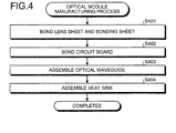
- FIG. 4 is a process flowchart of one example of a fabrication process of the optical module, using the flip-chip bonder. As depicted in FIG. 4 , in the fabrication process of the optical module, each of the following processes is performed, for example, by the flip-chip bonder.
- the process of bonding the lens sheet 120 and the bonding sheet 125 that are prepared beforehand is performed (step S401).
- the lens sheet 120 to be used at step S401 is one in which the lens 120a and the convex part 120b are integrally formed.
- the bonding sheet 125 to be used at step S401 is one in which the opening 125a is largely hollowed out by the cutting.
- the process is performed of bonding the flexible board 103 to the bonding sheet 125 of a formed body of the lens sheet 120 and the bonding sheet 125 bonded together at step S401 (step S402).
- the process is performed of mounting the optical waveguide 130 to the lens sheet 120 of the formed body of the flexible board 103, the lens sheet 120, and the bonding sheet 125 that were integrated at step S402 (step S403).
- the process is performed of mounting the heat sink 140 to the flexible board 103 of the formed body of the flexible board 103, the lens sheet 120, the bonding sheet 125, and the optical waveguide 130 that were integrated at step S403 (step S404). Then, the fabrication process is finished.
- step S401 since the lens sheet 120 with the convex part 120b formed thereon and the bonding sheet 125 with the opening 125a largely hollowed out by the cutting are used, the bonding sheet 125 and the lens sheet 120 can be bonded together even if the accurate alignment is not performed. This makes it possible to shorten the process time of step S401.
- processing may be such that the bonding of the flexible board 103 and the bonding sheet 125 at step S402 is performed firstly and the bonding of the lens sheet 120 at step S401 is performed thereafter.
- the alignment accuracy can be lowered.
- FIGs. 5A, 5B, and 5C are explanatory diagrams of one example of a fabrication process of the lens and the convex part.
- a mold 500 is used in the fabrication of the lens 120a and the convex part 120b.
- the mold 500 is intended to shape the arc-shaped lens 120a and the arc-shaped convex part 120b within a predetermined area.
- the distance between the lens 120a and the convex part 120b is specified to be, for example, 100 [ ⁇ m] or less. While details will be described later with reference to FIG. 6 , the mold 500 can form eight lenses 120a and four convex parts 120b simultaneously.
- the lens sheet 120 is pressurized against the mold 500 at high temperature. As depicted in FIG. 5C , by cooling the lens sheet 120 and pulling the lens sheet 120 away from the mold 500, the lens 120a and the convex part 120b are formed on the lens sheet 120.
- the convex part 120b as well as the lens 120a can be integrally formed in the process of forming the lens 120a. Namely, the convex part 120b can be formed without setting up a separate fabrication process. Since the convex part 120b is designed to have the same arc shape as that of the lens 120a, the mold is the easiest to fabricate and the cost can be reduced accordingly.
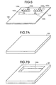
- FIG. 6 is an explanatory diagram of one example of the lens and the convex part. As depicted in FIG. 6 , two sets of four consecutive lenses 120a (eight in total) and a pair of convex parts 120b disposed around each set of lenses 120a (four in total) are formed in a predetermined area 120f on the lens sheet 120.
- the convex part 120b depicted here is one example.
- the number of the convex parts 120b is not limited to four but can be other numbers (see FIGs. 18 and 19 ) and the shape is not limited to the arc shape and may be a pillar shape (see FIG. 17 ).
- the way of the convex part 120b contacting with the flexible board 103 is not limited to a configuration of supporting by a point but can be a configuration of supporting by a line or a face (see FIGs. 13 to 16 ).
- FIGs. 7A and 7B is an explanatory diagram of one example of a fabrication process of the opening of the bonding sheet.
- the opening 125a is formed in the bonding sheet 125.
- the opening 125a is formed by cutting such as punching out of the bonding sheet 125 by use of edged tools such as a pinnacle blade.
- the minimum size of the cut-out part is rather large, on the order of 0.5 to 1.0 [mm].
- the opening 125a is formed at the position corresponding to the predetermined area 120f (see FIG. 6 ) in which the lenses 120a and the convex parts 120b are disposed on the lens sheet 120.
- the opening 125a can also be formed with high accuracy by a technique of masking the part other than the opening 125a of the bonding sheet 125 and dipping the bonding sheet 125 in an etching solution.
- this embodiment permits the opening 125a to be formed roughly, the punching-out technique can be used and the time required for the formation of the opening 125a can be shortened.
- FIGs. 8A and 8B are explanatory diagrams of one example of a process of bonding of the lens sheet and the bonding sheet.
- the process depicted in FIGs. 8A and 8B is the process depicted at step S401 of FIG. 4 .
- the process depicted in FIGs. 8A and 8B is the process of bonding together the lens sheet 120 formed in the process depicted in FIGs. 5A, 5B, and 5C and the bonding sheet 125 formed in the process depicted in FIGs. 7A and 7B .
- the lens sheet 120 and the bonding sheet 125 are bonded together in such a manner that the lenses 120a and the convex parts 120b will appear out of the opening 125a of the bonding sheet 125.
- the lens sheet 120 and the bonding sheet 125 are bonded together in such a manner that the bonding sheet 125 will not be layered over the lenses 120a or the convex parts 120b.
- the body formed by bonding of the lens sheet 120 and the bonding sheet 125 is used for the subsequent process (process at step S402 of FIG. 4 ).
- the lens sheet 120 and the bonding sheet 125 can be bonded together without the high-accuracy alignment in the process of bonding together of the lens sheet 120 and the bonding sheet 125. This makes it possible to shorten the process time in the bonding together of the lens sheet 120 and the bonding sheet 125.
- FIG. 9 is an explanatory diagram of one example of a process of bonding the flexible board.
- the process depicted in FIG. 9 is the process depicted at step S402 of FIG. 4 .
- the body formed by bonding together of the lens sheet 120 and the bonding sheet 125 depicted in FIGs. 8A and 8B and the flexible board 103 are aligned and bonded together by the flip-chip bonder.
- the light receiving element 111, the light emitting element 112, the TIA 113, and the driver IC 114 have been flip-chip-mounted to the flexible board 103.
- An electric wiring 103e is disposed on the flexible board 103.
- the alignment of the light receiving element 111 (light emitting element 112) and the lens 120a is performed with high accuracy.
- the body formed by bonding together of the lens sheet 120, the bonding sheet 125, and the flexible board 103 is used for the subsequent process (process at step S403 of FIG. 4 ).
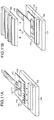
- FIGs. 10A and 10B are explanatory diagrams of one example of a process of mounting the optical waveguide.
- the process depicted in FIGs. 10A and 10B is the process depicted at step S403 of FIG. 4 .
- the optical waveguide 130 is mounted by the flip-chip bonder to the body formed by bonding together of the lens sheet 120, the bonding sheet 125, and the flexible board 103 depicted in FIG. 9 .
- the alignment of the lens 120a and the optical waveguide 130 is performed with high accuracy.
- the formed body including the lens sheet 120, the bonding sheet 125, the flexible board 103, and the optical waveguide 130 is used for the subsequent step (process at step S404 of FIG. 4 ).
- FIGs. 11A and 11B are explanatory diagrams of one example of a process of mounting the heat sink.
- the process depicted in FIGs. 11A and 11B is the process depicted at step S404 of FIG. 4 .
- the electric wiring 103e is connected to the electric connector 102.
- the heat sink 140 to cool the light receiving element 111 and the light emitting element 112 is mounted to the flexible board 103 by way of the heat dissipating sheet 141.
- the heat sink 140 is mounted to the flexible board 103 by clamps, screws, etc., not depicted.
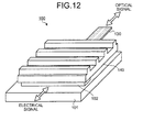
- FIG. 12 is an explanatory diagram of one example of a fabricated optical module.
- the heat sink 140 is mounted and is held in such a state as to pressurize the flexible board 103 by clamps, screws, etc., not depicted.
- the optical module 100 is arranged, for example, on a server board and is used as a device to convert the electrical signal to the light signal or convert the light signal to the electrical signal.
- the disposition of the convex part 120b on the lens sheet 120 makes it possible to reduce the warp, caused by the pressure of the heat sink 140, of such part of the flexible board 103 that corresponds to the void 125b.
- This makes it possible to reduce the misalignment of the light receiving element 111 with respect to the lens 120a.
- this can reduce the displacement of the light receiving element 111 in the height direction (direction in which the convex part 120b protrudes), the tilt of the light receiving element 111, and the horizontal displacement of the light receiving element 111 with respect to the lens. Therefore, an optical coupling loss can be reduced.
- the opening 125a can be formed rather largely in the process of forming the opening 125a of the bonding sheet 125 and the process time can be shortened in the process of forming the opening 125a.
- the opening 125a can be caused to come to the position of the lens 120a even if the accuracy is lowered of the bonding of the bonding sheet 125 and the lens sheet 120. This makes it possible to lower the accuracy of the bonding of the bonding sheet 125 and the lens sheet 120, shortening the process time at the time of the bonding of the bonding sheet 125 and the lens sheet 120. For this reason, the time consumed for the fabrication of the optical module 100 can be shortened.
- this embodiment uses the lens sheet 120 with the lens 120a and the convex part 120b integrally formed, it is made possible to make the lens 120a and the convex part 120b in the same process. Therefore, the convex part 120b can be formed without adding a separate process for making the convex part 120b. This makes it possible to make the convex part 120b while suppressing increases in the time consumed for the fabrication of the optical module 100.
- the reduction of the optical coupling loss as well as the shortening of the fabrication time can be achieved.
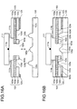
- FIGs. 13A and 13B are explanatory diagrams of variation 1 of the embodiment.
- Variation 1 differs from the above embodiment in the shape of the convex part 120b.
- the planar convex part 120b is formed on the lens sheet 120.
- the convex part 120b is thicker than the flat part 120c and is formed by the surface protruding above the flat part 120c.
- the convex part 120b may be arranged, for example, in a doughnut shape to surround the lens 120a.
- the convex part 120b is disposed at the position corresponding to the void 125b where the bonding sheet 125 is not disposed over the lens sheet 120 and at the position at which the convex part 120b abuts against the flexible board 103. This makes it possible to support such part of the flexible board 103 at which the bonding sheet 125 is not disposed from the lens sheet 120 side, reducing the warp of the flexible board 103 caused by the pressure of the heat sink 140.
- the lens 120a is disposed on the convex part 120b, using the upper surface of the convex part 120b formed in the planar state as a reference plane serving as a reference in the height direction.
- the distance between the lens 120a and the light receiving element 111 is set depending on the light receiving element to be used and a target focal spot size. For this reason, in variation 1, the lens 120a can be disposed close to the light receiving element 111 as compared with the case of disposing the lens 120a on the basis of the flat part 120c as in the above embodiment.
- Variation 1 it is made possible to set the distance short between the lens 120a and the light receiving element 111.
- Variation 1 makes it possible to expand the area supporting from the lens sheet 120 side such part of the flexible board 103 that corresponds to the void 125b, effectively reducing the warp of the flexible board 103. This makes it possible to reduce the misalignment of light receiving element 111 with respect to the lens 120a.
- FIGs. 14A and 14B are explanatory diagrams of variation 2 of the embodiment.
- the same components as those described in the above embodiment or variation 1 are given the same reference numerals used above, and the description thereof is omitted.
- Variation 2 differs from variation 1 in the lens 120a.
- the lens 120a is disposed on a reference surface 120d higher than the convex part 120b.
- Variation 2 enables the lens 120a to be disposed close to the light receiving element 111, as compared with variation 1. Therefore, variation 2 makes it possible to expand the area supporting from the lens sheet 120 side, a part of the flexible board 103 that corresponds to the void 125b, effectively reducing the warp of the flexible board 103. This makes it possible to set the distance shorter between the lens 120a and the light receiving element 111 while reducing the misalignment of the light receiving element 111 with respect to the lens 120a.
- the convex part 120b is specified to be in the planar state and thicker than the flat part 120c
- the convex part 120b is not limited to this and may be the arc-shaped convex part disposed on the flat part 120c as depicted in the above embodiment.
- configuration may be such that, continuous with the flat part 120c, the reference surface 120d is disposed to be is higher than the ark-shaped convex part 120b and on the reference surface 120d, the lens 120a will be disposed.
- FIGs. 15A and 15B are explanatory diagrams of variation 3 of the embodiment.
- the same components as those described in the above embodiment or variations 1 and 2 are given the same reference numerals used above, and description thereof is omitted.
- Variation 3 differs from variation 2 in the height of the reference surface 120d of the lens 120a.
- the lens 120a is disposed on the reference surface 120d that is lower than the convex part 120b and is also lower than the flat part 120c.
- Variation 3 enables the lens 120a to be disposed away from the light receiving element 111, as compared with the embodiment and variation 1. Therefore, variation 3 makes it possible to expand the area supporting from the lens sheet 120 side such part of the flexible board 103 that corresponds to the void 125b, effectively reducing the warp of the flexible board 103. This makes it possible to set the distance longer between the lens 120a and the light receiving element 111 while reducing the misalignment of the light receiving element 111 with respect to the lens 120a.
- the convex part 120b is specified to be in the planar state and thicker than the flat part 120c
- the convex part 120b is not limited to this and may be the arc-shaped convex part disposed on the flat part 120c as depicted in the above embodiment.
- configuration may be such that, continuous with the flat part 120c, the reference surface 120d is disposed to be lower than the flat part 120c and on the reference surface 120d, the lens 120a is disposed.
- the position of the lens 120a can be set freely depending on an optical element to be used and the target focal spot size.
- FIGs. 16A and 16B are explanatory diagrams of variation 4 of the embodiment.
- Variation 4 differs from the embodiment in that the convex part 120b abuts against the core layer 103b.
- the flexible board 103 has a non-formed part where the ground electrode 103c is not formed.
- the thickness of the convex part 120b formed on the lens sheet 120 may be determined as a total thickness of the thickness of the flat part 120c, the thickness of the bonding sheet 125, and the thickness of the ground electrode 103c.
- FIG. 17 is an explanatory diagram of variation 5 of the embodiment.
- Variation 5 differs from the embodiment in the shape of such part of the convex part 120b that abuts against the flexible board 103.
- the convex part 120b is formed in a pillar shape.
- An anti-slip part 120e is formed on the part (end) of the convex part 120b that abuts against the ground electrode 103c.
- the anti-slip part 120e is simply a knurled concavo-convex pattern formed on the part (end) of the convex part 120b that abuts against the ground electrode 103c. With the anti-slip part 120e shaped in the mold 500 that fabricates the convex part 120b, the anti-slip part 120e can be mold-formed simultaneously with the convex part 120b (see FIGs. 5A, 5B, and 5C ).
- Such a configuration can increase the frictional force by the anti-slip part 120e of the convex part 120b and can reduce the displacement of the light receiving element 111 (light emitting element 112).
- the surface of the ground electrode 103c has unevenness formed by the copper foil and has an anti-slip function due to the copper foil. For this reason, by causing the surface of the ground electrode 103c and the anti-slip part 120e to abut against each other, the frictional force can be further heightened.
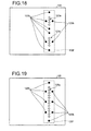
- FIG. 18 is an explanatory diagram of variation 6 of the embodiment.
- Variation 6 differs from the embodiment in the arrangement location and the number of the convex parts 120b. Though both of the lens 120a and the convex part 120b are transparent, the convex part 120b is indicated by a black circle for convenience of description in FIG. 18 .
- the convex part 120b is formed at each of four corners of a sequence of the lenses 120a (total eight convex parts 120b).
- the number of the convex parts 120b is larger by four than in the above embodiment. This can increase the number of places at which the part of the flexible board 103 where the bonding sheet 125 is not disposed is supported from the lens sheet 120 side. This makes it possible to reduce the warp of the flexible board 103 and to reduce the misalignment of the light receiving element 111 with respect to the lens 120a.
- FIG. 19 is an explanatory diagram of variation 7 of the embodiment.
- Variation 7 differs from variation 6 in the arrangement location of the lens 120a and the convex part 120b.
- 12 consecutive lenses 120a and eight convex parts 120b around them are formed within the predetermined area 120f on the lens sheet 120.
- the lens 120a is disposed depending on the number and the location of the optical element to be used (light receiving part 111a of light receiving element 111 and light emitting part 112a of light emitting element 112).
- Variation 7 depicts the lens sheet 120 to be used when 12 consecutive optical elements are disposed.
- a lens sheet 120 Even when the 12 consecutively disposed optical elements are used, such part of the flexible board 103 that corresponds to the void 125b can be supported from the lens sheet 120 side by the convex parts 120b. Therefore, it is made possible to effectively reduce the warp of the flexible board 103 caused by the pressure of the heat sink 140 and to reduce the misalignment of the light receiving element 111 with respect to the lens 120a.
- FIG. 20 is an explanatory diagram of variation 8 of the embodiment.
- Variation 8 differs from the above embodiment in the shape of the core layer 103b of the flexible board 103.
- the core layer 103b is a transparent member and is not the one having a hollowed-out part at the position corresponding to light path K.
- the core layer 103b transmits the signal light of light path K.
- the configuration using the core layer 103b of variation 8 can have the warp of the flexible board 103 caused by the pressure of the heat sink 140 at the void 125b where the bonding sheet 125 is not disposed.
- the core layer 103b according to variation 8 if the warp is caused to the flexible board 103, the core layer 103b becomes a point of reflection and the optical coupling loss becomes large.
- the lens sheet 120 with the convex part 120b disposed thereon it is made possible to support such part of the flexible board 103 that corresponds to the void 125b from the lens sheet 120 side, to reduce the warp of the flexible board 103, and to reduce the misalignment of the light receiving element 111 with respect to the lens 120a.
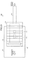
- FIG. 21 is an explanatory diagram of variation 9 of the embodiment.
- Variation 9 differs from the above embodiment in that neither the light emitting element 112 nor the driver IC 114 is disposed.
- the light receiving element 111 and the TIA 113 are mounted on the flexible board 103 of the optical module 100.
- the light receiving element 111 is pressurized by the heat sink 140.
- the heat sink 140 is disposed, with the heat dissipating sheet 141 sandwiched in between.
- the heat sink 140 cools the light receiving element 111 by way of the heat dissipating sheet 141.
- the heat sink 140 for example, by being fastened by clamps, screws, etc., to the flexible board 103, is held in such a state as to pressurize the light receiving element 111.
- Such a configuration enables the optical module to perform the optoelectric conversion of the light signal to the electrical signal.
- the convex part 120b on the lens sheet 120, it is made possible to reduce the warp of the flexible board 103 caused by the pressure of the heat sink 140 and to reduce the misalignment of the light receiving element 111 with respect to the lens 120a.
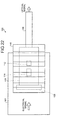
- FIG. 22 is an explanatory diagram of variation 10 of the embodiment.
- the same components as those described in the above embodiment are given the same reference numerals, and the description thereof is omitted.
- the variation 10 differs from the above embodiment in that neither the light receiving element 111 nor the TIA 113 is disposed.
- the light emitting element 112 and the driver IC 114 are mounted on the flexible board 103 of the optical module 100.
- the light emitting element 112 is pressurized by the heat sink 140.
- the heat sink 140 is disposed, with the heat dissipating sheet 141 sandwiched in between.
- the heat sink 140 cools the light emitting element 112 by way of the heat dissipating sheet 141.
- the heat sink 140 for example, by being fastened by clamps, screws, etc., to the flexible board 103, is held in such a state as to pressurize the light emitting element 112.
- Such a configuration enables the optical module to perform the optoelectric conversion of the electrical signal to the light signal.
- the convex part 120b on the lens sheet 120, it is made possible to reduce the warp of the flexible board 103 caused by the pressure of the heat sink 140 and to reduce the misalignment of the light emitting element 112 with respect to the lens 120a.
- FIG. 23 is an explanatory diagram of one example of the warp of the flexible board. As depicted in FIG. 23 , graph 2300 has the vertical axis representing the amount of warp [ ⁇ m] of the flexible board 103 and the horizontal axis representing the distance [mm] between support points supporting the flexible board 103 from downward.
- Curve 2302 indicates for reference the amount of warp of the flexible board 103 having the configuration of not disposing the convex part 120b (see FIG. 24 ).
- the distance between the support points depicted in curve 2302 corresponds to the distance between the bonding sheets 125 disposed opposite to each other across light path K (see FIG. 24 ).
- the distance between the support points (between bonding sheets 125) is on the order of 1 [mm] and the amount of warp of the flexible board 103 is on the order of 10 [ ⁇ m].
- curve 2301 indicates the amount of warp of the flexible board 103 having the configuration of disposing the convex part 120b depicted in the embodiment.
- the distance between the support points depicted in curve 2301 corresponds to the distance between the convex parts 120b disposed opposite to each other across light path K (see FIG. 3 ).
- the distance between the support points (between convex parts 120b) is on the order of 0.4 [mm] and the amount of warp of the flexible board 103 is on the order of 1 [ ⁇ m].
- FIG. 24 is an explanatory diagram of one example for reference of a configuration of not disposing the convex part on the lens sheet.
- the flexible board 103 is caused to warp by the pressure of the heat sink 140 against the light receiving element 111.
- the lengths L1 and L2, based on light path K, of the left and right voids 125b where the bonding sheet is not disposed can become L1 ⁇ L2.
- the warp of the flexible board 103 causes the light receiving element 111 to be inclined or to be displaced horizontally with respect to the lens, the optical coupling loss becomes prominent as compared with the case of displacement only in the Z direction in the drawing.
Landscapes
- Physics & Mathematics (AREA)
- General Physics & Mathematics (AREA)
- Optics & Photonics (AREA)
- Light Receiving Elements (AREA)
- Optical Couplings Of Light Guides (AREA)
- Semiconductor Lasers (AREA)
- Optical Integrated Circuits (AREA)
- Solid State Image Pick-Up Elements (AREA)
Applications Claiming Priority (1)
| Application Number | Priority Date | Filing Date | Title |
|---|---|---|---|
| JP2012254714A JP5910469B2 (ja) | 2012-11-20 | 2012-11-20 | 光モジュールおよびその製造方法 |
Publications (2)
| Publication Number | Publication Date |
|---|---|
| EP2733512A2 true EP2733512A2 (fr) | 2014-05-21 |
| EP2733512A3 EP2733512A3 (fr) | 2017-12-20 |
Family
ID=49170633
Family Applications (1)
| Application Number | Title | Priority Date | Filing Date |
|---|---|---|---|
| EP13184938.2A Withdrawn EP2733512A3 (fr) | 2012-11-20 | 2013-09-18 | Module optique et procédé de fabrication |
Country Status (4)
| Country | Link |
|---|---|
| US (1) | US9316799B2 (fr) |
| EP (1) | EP2733512A3 (fr) |
| JP (1) | JP5910469B2 (fr) |
| CN (1) | CN103837946B (fr) |
Families Citing this family (25)
| Publication number | Priority date | Publication date | Assignee | Title |
|---|---|---|---|---|
| JP2015050016A (ja) * | 2013-08-30 | 2015-03-16 | 東芝ライテック株式会社 | 発光モジュール及び照明装置 |
| JP6221540B2 (ja) * | 2013-09-13 | 2017-11-01 | 富士通株式会社 | 光デバイス、光モジュール、光デバイスの製造方法及び光モジュールの製造方法 |
| US9497570B2 (en) | 2014-02-06 | 2016-11-15 | Nimbelink Corp. | Embedded wireless modem |
| USD731491S1 (en) * | 2014-02-07 | 2015-06-09 | NimbeLink L.L.C. | Embedded cellular modem |
| US9470857B2 (en) * | 2014-06-13 | 2016-10-18 | Sumitomo Electric Industries, Ltd. | Optical module with beam splitter on reflecting surface |
| CN104540319B (zh) * | 2014-12-31 | 2017-08-25 | 苏州旭创科技有限公司 | 用于光模块的印刷电路板 |
| JP6477201B2 (ja) | 2015-04-27 | 2019-03-06 | 富士通株式会社 | 光モジュール |
| US10082638B2 (en) * | 2015-09-21 | 2018-09-25 | Lg Innotek Co., Ltd. | Lens driving unit, and a camera module and an optical appliance including the same |
| JP2017125956A (ja) * | 2016-01-14 | 2017-07-20 | 住友ベークライト株式会社 | レンズ付き光導波路、光電気混載基板、光モジュールおよび電子機器 |
| JP6711011B2 (ja) * | 2016-02-25 | 2020-06-17 | 住友ベークライト株式会社 | レンズ付き光導波路、光電気混載基板、光モジュールおよび電子機器 |
| JP2018010030A (ja) * | 2016-07-11 | 2018-01-18 | 富士通コンポーネント株式会社 | 光モジュール |
| JP2018017922A (ja) | 2016-07-28 | 2018-02-01 | 富士通コンポーネント株式会社 | 光モジュール及び光モジュールの製造方法 |
| US10591687B2 (en) | 2017-05-19 | 2020-03-17 | Adolite Inc. | Optical interconnect modules with 3D polymer waveguide |
| JP2019040011A (ja) | 2017-08-24 | 2019-03-14 | 富士通コンポーネント株式会社 | 光モジュール |
| JP2019078970A (ja) * | 2017-10-27 | 2019-05-23 | 富士通コンポーネント株式会社 | レンズシート及び光モジュール |
| JP2019083299A (ja) * | 2017-11-01 | 2019-05-30 | 富士通コンポーネント株式会社 | 光エンジン及び光モジュール |
| CN108535822A (zh) * | 2018-04-03 | 2018-09-14 | 中国科学院半导体研究所 | 光波导转向耦合结构组合体和光波导转向对准监控系统 |
| JP2020008813A (ja) * | 2018-07-12 | 2020-01-16 | 富士通コンポーネント株式会社 | 光モジュール |
| JP7059865B2 (ja) * | 2018-08-10 | 2022-04-26 | 富士通株式会社 | 光送信器 |
| JP7279338B2 (ja) * | 2018-10-31 | 2023-05-23 | 日本電気株式会社 | 光モジュールおよび光モジュールの製造方法 |
| KR102763576B1 (ko) * | 2019-07-24 | 2025-02-07 | 삼성전자주식회사 | 광학 센서 모듈을 포함하는 전자 장치 |
| CN114488423A (zh) * | 2020-10-27 | 2022-05-13 | 青岛海信宽带多媒体技术有限公司 | 一种光模块 |
| US11768338B2 (en) * | 2021-05-27 | 2023-09-26 | Taiwan Semiconductor Manufacturing Company, Ltd. | Optical interconnect structure, package structure and fabricating method thereof |
| CN117716268A (zh) | 2021-08-05 | 2024-03-15 | 住友电气工业株式会社 | 光模块和光连接器线缆 |
| DE112022003039T5 (de) * | 2021-08-05 | 2024-04-04 | Sumitomo Electric Industries, Ltd. | Optikmodul und optikverbindungskabel |
Citations (1)
| Publication number | Priority date | Publication date | Assignee | Title |
|---|---|---|---|---|
| JP2012068539A (ja) | 2010-09-24 | 2012-04-05 | Fujitsu Ltd | 光モジュールおよび製造方法 |
Family Cites Families (14)
| Publication number | Priority date | Publication date | Assignee | Title |
|---|---|---|---|---|
| JP4655674B2 (ja) * | 2005-02-28 | 2011-03-23 | ソニー株式会社 | 光電変換装置及びその製造方法、並びに光導波モジュール及び光情報処理装置 |
| TWI317030B (en) * | 2006-10-04 | 2009-11-11 | Ind Tech Res Inst | An optical interconnection module |
| US8189262B2 (en) * | 2007-01-25 | 2012-05-29 | Sumitomo Electric Fine Polymer, Inc. | Optical sheet, and mounting method and optical module using the optical sheet |
| CN101290921A (zh) * | 2007-04-17 | 2008-10-22 | 南茂科技股份有限公司 | 防止薄膜变形的薄膜覆晶封装基板 |
| BRPI0912695A2 (pt) * | 2008-05-13 | 2016-01-26 | Sharp Kk | dispositivo de fonte de luz, dispositivo de exibição, chassi e suporte lateral |
| JP5131023B2 (ja) * | 2008-05-15 | 2013-01-30 | 日立電線株式会社 | 光電気変換モジュール |
| JP5062056B2 (ja) * | 2008-06-25 | 2012-10-31 | 日立電線株式会社 | 光電気変換モジュール |
| JP2010122311A (ja) * | 2008-11-17 | 2010-06-03 | Hitachi Cable Ltd | レンズブロック及びそれを用いた光モジュール |
| US20110242435A1 (en) | 2008-12-18 | 2011-10-06 | Sharp Kabushiki Kaisha | Illumination device, display device, and television receiver |
| JP5093121B2 (ja) * | 2009-01-06 | 2012-12-05 | 日立電線株式会社 | 光モジュール |
| JP2011081071A (ja) * | 2009-10-05 | 2011-04-21 | Hitachi Cable Ltd | 光モジュール |
| EP2428828B1 (fr) * | 2010-09-13 | 2016-06-29 | Tyco Electronics Svenska Holdings AB | Module optique haute vitesse miniaturisé |
| JP2012108326A (ja) | 2010-11-17 | 2012-06-07 | Three M Innovative Properties Co | マイクロレンズシート材とその製造方法 |
| JP5664905B2 (ja) * | 2011-01-18 | 2015-02-04 | 日立金属株式会社 | 光電変換モジュール |
-
2012
- 2012-11-20 JP JP2012254714A patent/JP5910469B2/ja not_active Expired - Fee Related
-
2013
- 2013-09-03 US US14/016,603 patent/US9316799B2/en not_active Expired - Fee Related
- 2013-09-18 EP EP13184938.2A patent/EP2733512A3/fr not_active Withdrawn
- 2013-09-30 CN CN201310460470.1A patent/CN103837946B/zh not_active Expired - Fee Related
Patent Citations (1)
| Publication number | Priority date | Publication date | Assignee | Title |
|---|---|---|---|---|
| JP2012068539A (ja) | 2010-09-24 | 2012-04-05 | Fujitsu Ltd | 光モジュールおよび製造方法 |
Also Published As
| Publication number | Publication date |
|---|---|
| CN103837946A (zh) | 2014-06-04 |
| JP5910469B2 (ja) | 2016-04-27 |
| CN103837946B (zh) | 2015-11-18 |
| US9316799B2 (en) | 2016-04-19 |
| JP2014102399A (ja) | 2014-06-05 |
| US20140140657A1 (en) | 2014-05-22 |
| EP2733512A3 (fr) | 2017-12-20 |
Similar Documents
| Publication | Publication Date | Title |
|---|---|---|
| US9316799B2 (en) | Optical module and fabrication method | |
| US10436991B2 (en) | Optical interconnect modules based on glass substrate with polymer waveguide | |
| US8774576B2 (en) | Optical module and method for manufacturing the same | |
| CN100410710C (zh) | 光模块及其制造方法、光通信装置、集成电路、电路板、电子设备 | |
| US8041159B2 (en) | Optical/electrical hybrid substrate and method of manufacturing the same | |
| KR101924939B1 (ko) | 슬림형 커넥터 플러그, 이를 이용한 액티브 광 케이블 조립체 및 그의 제조방법 | |
| US9581772B2 (en) | Optical electrical module used for optical communication | |
| US9054024B2 (en) | Apparatus and method for optical communications | |
| JPWO2008139763A1 (ja) | 光通信モジュールとその製造方法及び光送受信装置 | |
| US11852877B2 (en) | Connector plug and active optical cable assembly using same | |
| JP2006091241A (ja) | 光電気複合配線部品及びこれを用いた電子機器 | |
| WO2013046416A1 (fr) | Module optique | |
| US20050025435A1 (en) | Optical module and manufacturing method of the same, optical-communication apparatus, and electronic apparatus | |
| KR101918197B1 (ko) | 슬림형 커넥터 플러그, 이를 이용한 액티브 광 케이블 조립체 및 그의 제조방법 | |
| KR102206368B1 (ko) | 커넥터 플러그 및 이를 이용한 액티브 광 케이블 조립체 | |
| US8861903B2 (en) | Method of manufacturing optical waveguide device and optical waveguide device | |
| JP2008010837A (ja) | 光通信モジュールとその製造方法及び光送受信装置 | |
| JP2010097169A (ja) | 光電気モジュール、光基板および光電気モジュール製造方法 | |
| CN115113349A (zh) | 光子系统及其制造方法 | |
| JP2007101571A (ja) | 光ケーブル及び送受信サブアセンブリ | |
| KR20050072736A (ko) | 연성 광 pcb를 이용한 광연결 장치 | |
| JP2012226100A (ja) | 光回路 | |
| JP2008134444A (ja) | 光モジュール及び光導波路構造体 | |
| CN102736192A (zh) | 光电混载基板及其制造方法 | |
| JP4659082B2 (ja) | 光電気複合配線部品及びこれを用いた電子機器 |
Legal Events
| Date | Code | Title | Description |
|---|---|---|---|
| PUAI | Public reference made under article 153(3) epc to a published international application that has entered the european phase |
Free format text: ORIGINAL CODE: 0009012 |
|
| 17P | Request for examination filed |
Effective date: 20130918 |
|
| AK | Designated contracting states |
Kind code of ref document: A2 Designated state(s): AL AT BE BG CH CY CZ DE DK EE ES FI FR GB GR HR HU IE IS IT LI LT LU LV MC MK MT NL NO PL PT RO RS SE SI SK SM TR |
|
| AX | Request for extension of the european patent |
Extension state: BA ME |
|
| PUAL | Search report despatched |
Free format text: ORIGINAL CODE: 0009013 |
|
| AK | Designated contracting states |
Kind code of ref document: A3 Designated state(s): AL AT BE BG CH CY CZ DE DK EE ES FI FR GB GR HR HU IE IS IT LI LT LU LV MC MK MT NL NO PL PT RO RS SE SI SK SM TR |
|
| AX | Request for extension of the european patent |
Extension state: BA ME |
|
| RIC1 | Information provided on ipc code assigned before grant |
Ipc: G02B 6/43 20060101ALI20171113BHEP Ipc: G02B 6/42 20060101AFI20171113BHEP |
|
| STAA | Information on the status of an ep patent application or granted ep patent |
Free format text: STATUS: THE APPLICATION IS DEEMED TO BE WITHDRAWN |
|
| 18D | Application deemed to be withdrawn |
Effective date: 20180621 |