EP2733747A2 - Solarzelle - Google Patents
Solarzelle Download PDFInfo
- Publication number
- EP2733747A2 EP2733747A2 EP13187594.0A EP13187594A EP2733747A2 EP 2733747 A2 EP2733747 A2 EP 2733747A2 EP 13187594 A EP13187594 A EP 13187594A EP 2733747 A2 EP2733747 A2 EP 2733747A2
- Authority
- EP
- European Patent Office
- Prior art keywords
- electrode layer
- region
- solar cell
- back surface
- layer
- Prior art date
- Legal status (The legal status is an assumption and is not a legal conclusion. Google has not performed a legal analysis and makes no representation as to the accuracy of the status listed.)
- Withdrawn
Links
Images


Classifications
-
- H—ELECTRICITY
- H10—SEMICONDUCTOR DEVICES; ELECTRIC SOLID-STATE DEVICES NOT OTHERWISE PROVIDED FOR
- H10F—INORGANIC SEMICONDUCTOR DEVICES SENSITIVE TO INFRARED RADIATION, LIGHT, ELECTROMAGNETIC RADIATION OF SHORTER WAVELENGTH OR CORPUSCULAR RADIATION
- H10F71/00—Manufacture or treatment of devices covered by this subclass
-
- H—ELECTRICITY
- H10—SEMICONDUCTOR DEVICES; ELECTRIC SOLID-STATE DEVICES NOT OTHERWISE PROVIDED FOR
- H10F—INORGANIC SEMICONDUCTOR DEVICES SENSITIVE TO INFRARED RADIATION, LIGHT, ELECTROMAGNETIC RADIATION OF SHORTER WAVELENGTH OR CORPUSCULAR RADIATION
- H10F10/00—Individual photovoltaic cells, e.g. solar cells
- H10F10/10—Individual photovoltaic cells, e.g. solar cells having potential barriers
- H10F10/16—Photovoltaic cells having only PN heterojunction potential barriers
- H10F10/167—Photovoltaic cells having only PN heterojunction potential barriers comprising Group I-III-VI materials, e.g. CdS/CuInSe2 [CIS] heterojunction photovoltaic cells
-
- H—ELECTRICITY
- H10—SEMICONDUCTOR DEVICES; ELECTRIC SOLID-STATE DEVICES NOT OTHERWISE PROVIDED FOR
- H10F—INORGANIC SEMICONDUCTOR DEVICES SENSITIVE TO INFRARED RADIATION, LIGHT, ELECTROMAGNETIC RADIATION OF SHORTER WAVELENGTH OR CORPUSCULAR RADIATION
- H10F19/00—Integrated devices, or assemblies of multiple devices, comprising at least one photovoltaic cell covered by group H10F10/00, e.g. photovoltaic modules
- H10F19/30—Integrated devices, or assemblies of multiple devices, comprising at least one photovoltaic cell covered by group H10F10/00, e.g. photovoltaic modules comprising thin-film photovoltaic cells
- H10F19/31—Integrated devices, or assemblies of multiple devices, comprising at least one photovoltaic cell covered by group H10F10/00, e.g. photovoltaic modules comprising thin-film photovoltaic cells having multiple laterally adjacent thin-film photovoltaic cells deposited on the same substrate
- H10F19/33—Patterning processes to connect the photovoltaic cells, e.g. laser cutting of conductive or active layers
-
- H—ELECTRICITY
- H10—SEMICONDUCTOR DEVICES; ELECTRIC SOLID-STATE DEVICES NOT OTHERWISE PROVIDED FOR
- H10F—INORGANIC SEMICONDUCTOR DEVICES SENSITIVE TO INFRARED RADIATION, LIGHT, ELECTROMAGNETIC RADIATION OF SHORTER WAVELENGTH OR CORPUSCULAR RADIATION
- H10F71/00—Manufacture or treatment of devices covered by this subclass
- H10F71/138—Manufacture of transparent electrodes, e.g. transparent conductive oxides [TCO] or indium tin oxide [ITO] electrodes
-
- H—ELECTRICITY
- H10—SEMICONDUCTOR DEVICES; ELECTRIC SOLID-STATE DEVICES NOT OTHERWISE PROVIDED FOR
- H10F—INORGANIC SEMICONDUCTOR DEVICES SENSITIVE TO INFRARED RADIATION, LIGHT, ELECTROMAGNETIC RADIATION OF SHORTER WAVELENGTH OR CORPUSCULAR RADIATION
- H10F77/00—Constructional details of devices covered by this subclass
- H10F77/20—Electrodes
- H10F77/206—Electrodes for devices having potential barriers
- H10F77/211—Electrodes for devices having potential barriers for photovoltaic cells
-
- H—ELECTRICITY
- H10—SEMICONDUCTOR DEVICES; ELECTRIC SOLID-STATE DEVICES NOT OTHERWISE PROVIDED FOR
- H10F—INORGANIC SEMICONDUCTOR DEVICES SENSITIVE TO INFRARED RADIATION, LIGHT, ELECTROMAGNETIC RADIATION OF SHORTER WAVELENGTH OR CORPUSCULAR RADIATION
- H10F77/00—Constructional details of devices covered by this subclass
- H10F77/20—Electrodes
- H10F77/244—Electrodes made of transparent conductive layers, e.g. transparent conductive oxide [TCO] layers
-
- H—ELECTRICITY
- H10—SEMICONDUCTOR DEVICES; ELECTRIC SOLID-STATE DEVICES NOT OTHERWISE PROVIDED FOR
- H10F—INORGANIC SEMICONDUCTOR DEVICES SENSITIVE TO INFRARED RADIATION, LIGHT, ELECTROMAGNETIC RADIATION OF SHORTER WAVELENGTH OR CORPUSCULAR RADIATION
- H10F77/00—Constructional details of devices covered by this subclass
- H10F77/40—Optical elements or arrangements
- H10F77/42—Optical elements or arrangements directly associated or integrated with photovoltaic cells, e.g. light-reflecting means or light-concentrating means
- H10F77/48—Back surface reflectors [BSR]
-
- Y—GENERAL TAGGING OF NEW TECHNOLOGICAL DEVELOPMENTS; GENERAL TAGGING OF CROSS-SECTIONAL TECHNOLOGIES SPANNING OVER SEVERAL SECTIONS OF THE IPC; TECHNICAL SUBJECTS COVERED BY FORMER USPC CROSS-REFERENCE ART COLLECTIONS [XRACs] AND DIGESTS
- Y02—TECHNOLOGIES OR APPLICATIONS FOR MITIGATION OR ADAPTATION AGAINST CLIMATE CHANGE
- Y02E—REDUCTION OF GREENHOUSE GAS [GHG] EMISSIONS, RELATED TO ENERGY GENERATION, TRANSMISSION OR DISTRIBUTION
- Y02E10/00—Energy generation through renewable energy sources
- Y02E10/50—Photovoltaic [PV] energy
- Y02E10/52—PV systems with concentrators
-
- Y—GENERAL TAGGING OF NEW TECHNOLOGICAL DEVELOPMENTS; GENERAL TAGGING OF CROSS-SECTIONAL TECHNOLOGIES SPANNING OVER SEVERAL SECTIONS OF THE IPC; TECHNICAL SUBJECTS COVERED BY FORMER USPC CROSS-REFERENCE ART COLLECTIONS [XRACs] AND DIGESTS
- Y02—TECHNOLOGIES OR APPLICATIONS FOR MITIGATION OR ADAPTATION AGAINST CLIMATE CHANGE
- Y02E—REDUCTION OF GREENHOUSE GAS [GHG] EMISSIONS, RELATED TO ENERGY GENERATION, TRANSMISSION OR DISTRIBUTION
- Y02E10/00—Energy generation through renewable energy sources
- Y02E10/50—Photovoltaic [PV] energy
- Y02E10/541—CuInSe2 material PV cells
-
- Y—GENERAL TAGGING OF NEW TECHNOLOGICAL DEVELOPMENTS; GENERAL TAGGING OF CROSS-SECTIONAL TECHNOLOGIES SPANNING OVER SEVERAL SECTIONS OF THE IPC; TECHNICAL SUBJECTS COVERED BY FORMER USPC CROSS-REFERENCE ART COLLECTIONS [XRACs] AND DIGESTS
- Y02—TECHNOLOGIES OR APPLICATIONS FOR MITIGATION OR ADAPTATION AGAINST CLIMATE CHANGE
- Y02P—CLIMATE CHANGE MITIGATION TECHNOLOGIES IN THE PRODUCTION OR PROCESSING OF GOODS
- Y02P70/00—Climate change mitigation technologies in the production process for final industrial or consumer products
- Y02P70/50—Manufacturing or production processes characterised by the final manufactured product
Definitions
- An aspect of the present invention relates to a solar cell.
- a copper-indium-gallium-(di)selenide (CIGS) solar cell is a solar cell that can be implemented as a thin film and does not use Si.
- CIGS solar cell will play an important role in the spread of solar energy by lowering the production cost of solar cells.
- CIGS solar cells are thermally stable, a decrease in efficiency hardly occurs as time elapses. Therefore, various studies have been conducted to increase the power-generating capacity of CIGS solar cells.
- Embodiments provide a solar cell capable of improving power generation efficiency while being implemented to be thin.
- a solar cell including: a substrate; a back surface electrode layer formed on the substrate in which a 1a-th through-region is formed; a transparent electrode layer formed on the back surface electrode layer in which a 1b-th through-region is formed at a position corresponding to the 1a-th through-region; and a light absorbing layer formed on the transparent electrode layer.
- the 1a-th through-region is formed by patterning the back surface electrode layer, and the 1b-th through-region is formed by patterning the transparent electrode layer.
- the transparent electrode layer is extended to cover the upper surface of the back surface electrode layer and the side surface of the back surface electrode layer exposed by the 1a-th through-region.
- the transparent electrode layer is formed to extend on the upper surface of the substrate exposed by the 1a-th through-region. That is, the transparent electrode layer is formed to further extend on the upper surface of the substrate exposed by the 1a-th through-region, such that the transparent electrode layer covers an area of the substrate that is greater than the width of said transparent electrode layer that covers the side surface of the back surface electrode layer exposed by the 1a-th through-region.
- the width of the 1b-th through-region is narrower than that of the corresponding 1a-th through-region.
- the difference in width between the 1a-th through-region and the 1b-the through-region is 10 ⁇ m or more.
- the difference in width between the 1a-th through-region and the first through-region is 30 ⁇ m or more.
- the back surface electrode layer includes at least one of Ag, A1, Cu, Au, Pt and Cr.
- the solar cell further includes an adhesion improving layer formed between the back surface electrode layer and the substrate.
- the adhesion improving layer includes at least one of Ti, Cr, Mo and Ni.
- the solar cell further includes a diffusion barrier layer formed between the back surface electrode layer and the substrate.
- the diffusion barrier layer includes at least one of oxide and nitride materials.
- the diffusion barrier layer includes at least one of SiO x , SiN x , SiO x N y , Al 2 O 3 , AlO x N y , TiN, TaN and WN.
- the diffusion barrier layer be formed between the back surface electrode layer and the substrate and on the upper surface of the substrate, exposed by the 1a-th through-region.
- the solar cell further includes a contact resistance improving layer formed between the transparent electrode layer and the light absorbing layer.
- the contact resistance improving layer includes at least one of MSe x and MS x (here, M is any one of Mo, W, Ta, Nb, Ti, Cr, V and Mn).
- the solar cell further includes a buffer layer formed on the light absorbing layer, and a rear surface electrode layer formed on the buffer layer.
- a first aspect of the invention relates to a solar cell as described in Claim 1. Embodiments of this first aspect may be found in Claims 2 to 14.
- a second aspect of the invention relates to a method for forming the solar cell according to Claims 1 to 14.
- a transparent electrode layer is formed between a back surface electrode layer and a light absorbing layer, so that it is possible to implement a thin solar cell and to improve power generation efficiency.
- the back surface electrode layer is configured as a high reflection electrode, thereby improving the re-absorption rate of the solar cell.
- the exposed back surface electrode layer is covered with the transparent electrode layer, so that it is possible to prevent selenization of the back surface electrode layer. Accordingly, it is possible to prevent a decrease in resistance of the back surface electrode layer, a peeling phenomenon and a defect caused by diffusion of the high reflection electrode into the light absorbing layer.
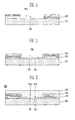
- FIG. 1 is a sectional view of a solar cell according to an embodiment of the present invention.
- FIGS. 2 and 3 are sectional views comparing solar cells with the solar cell shown in FIG. 1 .
- FIGS. 4 to 6 are sectional views illustrating a fabricating method of the solar cell shown in FIG. 1 .
- FIG. 7 is a sectional view of a solar cell according to another embodiment of the present invention.
- FIGS. 8 to 11 are sectional views of solar cells according to still other embodiments of the present invention.
- FIG. 1 is a sectional view of a solar cell 100 according to an embodiment of the present invention.
- the solar cell 100 according to this embodiment will be described with reference to FIG. 1 .
- the solar cell 100 sequentially includes a substrate 110, a back surface electrode layer 120 in which a 1a-th through-hole 121 is formed, a transparent electrode layer 130 in which a 1b-th through-hole 131 is formed, and a light absorbing layer 140.
- the substrate 110 is a member that provides a space in which the back surface electrode layer 120 and the transparent electrode layer 130 are formed.
- the substrate 110 becomes a base of the solar cell 100.
- the substrate 110 is a glass substrate, ceramic substrate, metal substrate, polymer substrate, etc.
- the substrate 110 is a glass substrate including alkali elements such as Na, K and Cs therein.
- the substrate 110 is a sodalime glass substrate or high strained point soda glass substrate.
- the back surface electrode layer 120 is a member which is formed on the substrate 110, and includes the 1a-th through-region 121.
- the 1a-th through-hole 121 is formed in the back surface electrode layer 120 through a patterning process.
- the 1a-th through-region 121 means a through-hole or a space in which the patterned back surface electrode layers 120 are spaced apart from each other.
- the back surface electrode layer 120 is made of metal having excellent stability at a high temperature and high electrical conductivity.
- the back surface electrode layer 120 is made of high reflection metal such as Ag, Al, Cu, Pt or Cr.
- the high reflection metal is used as the back surface electrode layer 120 in this embodiment, the reflectivity of light transmitted into the solar cell 100 is high even though the solar cell 100 is implemented to be thin. Thus, the amount of light reabsorbed in the solar cell 100 increases, thereby reducing current loss.
- the transparent electrode layer 130 is a member formed on the back surface electrode layer 120 having the 1a-th through-region 121 formed therein.
- the 1b-th through-region 131 is formed in the transparent electrode layer 130 through a patterning process.
- the 1b-th through-region 131 is formed at a position corresponding to the 1a-th through-region 121.
- a portion of the substrate 110 is exposed by the 1b-th through-region 131, so as to contact the light absorbing layer 140.
- the width of the 1b-th through-region 131 is narrower than that of the 1a-th through-region 121, and the difference in width between the 1a-th through-region 121 and the 1b-th through-region 131 is 10 ⁇ m or more.
- the difference in width between the 1a-th through-region 121 and the 1b-th through-region 131 is set to 30 ⁇ m or more.
- the transparent electrode layer 130 is positioned to extend to the upper surface of the back surface electrode layer 120, the side surface of the back surface electrode layer 120, exposed by the 1a-th through-region 121, and a portion of the upper surface of the substrate 110, exposed by the 1a-th through-region 121.
- the transparent electrode layer 130 is positioned at a portion adjacent to the back surface electrode layer 120 on the upper surface of the substrate 110 is that the 1b-th through-region 131 is positioned to correspond to the 1a-th through-region 121.
- the transparent electrode layer 130 is formed to have, for example, a thickness of 50 to 150nm.
- the thickness of the transparent electrode layer 130 positioned at the exposed side surface of the back surface electrode layer 120 is, for example, 10nm or more in order to prevent a selenization reaction between the back surface electrode layer 120 and the light absorbing layer 140.
- the present invention is not limited. Specifically, a case where the width of the 1b-th through-region 131 is implemented to be slightly narrower than that of the 1a-th through-region 121, so that the transparent electrode layer 130 is formed on only the upper and side surfaces of the back surface electrode layer 120 is included in the present invention.
- a transparent and conductive material is preferably used for the transparent electrode layer 130 in terms of the improvement of high reflectivity and refractive index
- the transparent electrode layer 130 is made of, for example, transparent conductive oxide (TOC).
- the transparent electrode layer 130 is made of ZnO or ZnO doped with Al, Ga, B, etc.
- the transparent electrode layer 130 is made of In 2 O 3 , SnO 2 , TiO 2 , etc.
- the light absorbing layer 140 is a member which is formed on the transparent electrode layer 130 having the 1b-th through-region 131 formed therein.
- the light absorbing layer 140 is a portion absorbing light, and is formed of a Group I-III-VI based compound semiconductor or Group I-II-IV-VI based compound semiconductor.
- the Group I element is any one of Cu, Ag, Au, etc.
- the Group II element is any one of Zn, Cd, etc.
- the Group III element is any one of In, Ga, Al, etc.
- the Group IV element is any one of Si, Ge, Sn, Pb, etc.
- the Group VI element is any one of S, Se, Te, etc.
- the Group I-III-VI based compound semiconductor is, for example, a compound semiconductor such as CIS, CGS or CIGS (here, C denotes copper (Cu), I denotes indium (In), G denotes gallium (Ga), and S denotes one or more of sulfur (S) and selenium (Se)).
- the Group I-II-IV-VI based compound semiconductor is a compound semiconductor such as CZTS (here, C denotes copper (Cu), Z denotes zinc (Zn), T denotes tin (Sn), and S denotes one or more of sulfur (S) and selenium (Se)).
- FIGS. 2 and 3 are sectional views comparing prior art solar cells with the solar cell 100 shown in FIG. 1 .
- the solar cell 100 according to this embodiment will be described in a more detailed manner with reference to the prior art embodiments shown in FIGS. 2 and 3 .
- a general back surface electrode layer 12 formed on a substrate 11 of a solar cell 10 is made of molybdenum (Mo).
- Mo molybdenum
- the Mo is stable under the selenization atmosphere of a light absorbing layer 14, but the reflectivity of the Mo is relatively low. Therefore, in a case where the thickness of the solar cell 10 is implemented to be thin, the re-absorption of light is inferior. Particularly, in a case where the solar cell 10 is implemented to have a thickness of 1 ⁇ m or less, current loss of a few mA/cm 2 is expected.
- reference numeral 13 denotes an alloy layer, and corresponds to a layer formed by a selenization reaction between the Mo and the light absorbing layer 14.
- a solar cell 20 using high reflection metal such as Ag as a back surface electrode layer 22 formed on a substrate 21 has been considered as shown in FIG. 3 .
- a high reflection metal such as Ag is unstable under a selenization atmosphere of 400°C or more, and therefore, the entire back surface electrode layer 22 may be converted into AgSe x .
- the resistance of the back surface electrode layer 22 is lost, and the AgSe x has a low adhesive property with the substrate 21. Therefore, as shown in FIG. 3 , a peeling phenomenon may occur in a subsequent process.
- the Ag of the back surface electrode layer 22 is diffused in a light absorbing layer 24 configured with CIGS, and therefore, a defect may occur in the light absorbing layer 24.
- the solar cell 100 according to the currently described embodiment is derived from such a viewpoint, and all the problems described above can be solved in the solar cell 100 shown in FIG. 1 .
- the solar cell 100 is implemented to have a thickness of 0.5 ⁇ m or less using high reflection metal such as Ag or Al as the back surface electrode layer 120, current loss is low, thereby increasing the re-absorption rate of light.
- the transparent electrode layer 130 is formed after the 1a-th through-region 121 is formed in the back surface electrode layer 120, and thus it is possible to prevent the back surface electrode layer 120 and the light absorbing layer 140 from coming in direct contact with each other.
- the transparent electrode layer 130 is formed not only on the upper surface of the back surface electrode layer 120 but also the exposed side surface of the back surface electrode layer 120, so that it is possible to prevent, in advance, the high reflection metal such as Ag and the Se of the light absorbing layer 140 from reacting with each other through the exposed side surface of the back surface electrode layer 120.
- the entire back surface electrode layer 120 from being transferred into AgSe x due to the reaction between Se and Ag through the exposed side surface of the back surface electrode layer 120. Accordingly, it is possible to prevent resistance loss due to the transfer of the back surface electrode layer into AgSe x , occurrence of a peeling phenomenon, occurrence of a defect, etc.
- the transparent electrode layer 130 is also formed on the upper surface of the substrate 110, exposed by the 1a-th through-region 121. This is because the width of the 1a-th through-region 121 is wider than that of the 1b-th through-region 131. In a case where the transparent electrode layer 130 is formed to extend up to the upper surface of the substrate 110, it is possible to more certainly prevent the high reflection metal from reacting with the Se of the light absorbing layer 140.
- FIGS. 4 to 6 are sectional views illustrating a fabricating method of the solar cell 100 shown in FIG. 1 .
- the fabricating method of the solar cell 100 according to this embodiment will be described with reference to FIGS. 4 to 6 .
- a patterned back surface electrode layer 120 is formed on the upper surface of a substrate 110.
- a 1a-th through region 121 is formed in the back surface electrode layer through a patterning process, and a portion of the upper surface of the substrate 110 is exposed to the outside by the 1a-th through-region 121.
- the back surface electrode layer 120 is formed through a sputtering, deposition, plating or screen printing process, and the 1a-th through-region 121 is formed through, for example, a laser process.
- a transparent electrode layer 130 is formed on the back surface electrode layer 120 having the 1a-th through-region 121 formed therein.
- a 1b-th through-region 131 is formed in the transparent electrode layer 130 through a patterning process.
- the 1b-th through-region 131 is formed to correspond to the position at which the 1a-th through-region 121 is formed.
- the transparent electrode layer 130 is formed through a sputtering, deposition or chemical vapor deposition (CVD) process, and the 1b-th through-region 131 is formed through a laser process.
- the width of the 1b-th through-region 131 is narrower by 10 or more, preferably 30 or more than that of the 1a-th through-region 121, in consideration of mechanical tolerance according to the laser process.
- a light absorbing layer 140 is formed on the transparent electrode layer 130 having the 1b-th through-region 131 formed therein, thereby fabricating the solar cell 100.
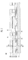
- FIG. 7 is a sectional view of a solar cell 200 according to another embodiment of the present invention.
- the solar cell 200 according to this embodiment will be described with reference to FIG. 7 .
- the solar cell 200 includes a substrate 210, a back surface electrode layer 220 in which a 1a-th through-region is formed, a transparent electrode layer 230 in which a 1b-th through-region 231 is formed, and a light absorbing layer 240, as shown in FIG. 1 .
- the solar cell 200 further includes a buffer layer 250 and a rear surface electrode layer 260.
- the buffer layer 250 is formed with at least one layer on the light absorbing layer 240.
- the light absorbing layer 240 formed beneath the buffer layer 250 acts as a p-type semiconductor
- the rear surface electrode layer 260 formed on the buffer layer 250 acts as an n-type semiconductor, so that a p-n junction can be formed between the light absorbing layer 240 and the rear surface electrode layer 260.
- the buffer layer 250 is formed to have a bandgap at a middle level between those of the light absorbing layer 240 and the rear surface electrode layer 260, so that an excellent junction between the light absorbing layer 240 and the rear surface electrode layer 260 can be implemented.
- the buffer layer 250 is made of CdS, ZnS, etc.
- the buffer layer 250 is patterned together with the light absorbing layer 240. Accordingly, the buffer layer 250 includes a second through-region 251.
- the rear surface electrode layer 260 is formed on the buffer layer 260.
- the rear surface electrode layer 260 is a conductive layer, and acts as an n-type semiconductor.
- the rear surface electrode layer 260 is made of TOC.
- the rear surface electrode layer 260 is made of ZnO.
- the rear surface electrode layer 260 is also patterned together with the buffer layer 250 and the light absorbing layer 240. Accordingly, the rear surface electrode layer 260 includes a third through-region 261.
- FIGS. 8 to 11 are sectional views of solar cells 300, 400, 500 and 600 according to still other embodiments of the present invention.
- the solar cells 300, 400, 500 and 600 according to these embodiments will be described with reference to FIGS. 8 to 11 .
- the solar cell 300 includes a substrate 310, a back surface electrode layer 320 in which a 1a-th through-region 321 is formed, a transparent electrode layer 330 in which a 1b-th through-region 331 is formed, and a light absorbing layer 340, as described in FIG. 1 .
- the solar cell 300 further includes an adhesion improving layer 350.
- the adhesion improving layer 350 is interposed between the back surface electrode layer 320 and the substrate 310.
- the adhesion improving layer 350 is a member for improving the adhesion between the substrate 310 and the back surface electrode layer 320 made of high reflection metal.
- the adhesion improving layer 350 is formed between the substrate 310 and a portion at which the 1a-th through-region 321 is not formed in the back surface electrode layer 310.
- the adhesion improving layer 350 includes at least one of Ti, Cr, Mo and Ni.
- the adhesion improving layer 350 is formed before the formation of the back surface electrode layer 320.
- the adhesion improving layer 350 is patterned together with the back surface electrode layer 320 when the 1a-th through-region 321 is formed after the formation of the back surface electrode layer 320.
- the solar cell 400 includes a substrate 410, a back surface electrode layer 420 in which a 1a-th through-region 421 is formed, a transparent electrode layer 430 in which a 1b-th through-region 431 is formed, and a light absorbing layer 440, as described in FIG. 1 .
- the solar cell 400 further includes a diffusion barrier layer 450.
- the diffusion barrier layer 450 is formed between the back surface electrode layer 420 and the substrate 410. More specifically, the diffusion barrier layer 450 is formed between the substrate 410 and a portion at which the 1a-th through-region 421 is not formed in the back surface electrode layer 420.
- the diffusion barrier layer 450 is a member for preventing alkali ions such as Na or K ions, or Fe ions from being diffused from the substrate 410.
- the diffusion barrier layer 450 includes at least one of oxide and nitride materials such as SiO x , SiN x , SiO x N y , Al 2 O 3 , AlO x N y , TiN, TaN and WN.
- the diffusion barrier layer 450 is formed before the formation of the back surface electrode layer 420.
- the diffusion barrier layer 450 is patterned together with the back surface electrode layer 420 when the 1a-th through-region 421 is formed after the formation of the back surface electrode layer 420.
- the solar cell 500 includes a substrate 510, a back surface electrode layer 520 in which a 1a-th through-region 521 is formed, a transparent electrode layer 530 in which a 1b-th through-region 531 is formed, and a light absorbing layer 540, as described in FIG. 1 .
- the solar cell 500 further includes a diffusion barrier layer 550.
- the diffusion barrier layer 550 is formed between the substrate 510 and the back surface electrode layer 520. Unlike FIG. 9 , the diffusion barrier layer 550 is also formed on the upper surface of the substrate 510 having the 1a-th through-region 521 formed thereon. In this embodiment, the diffusion barrier layer 550 is also formed on the upper surface of the substrate 510 having the 1a-th through-region 521 formed thereon, and thus it is possible to prevent impurities from being diffused through the 1a-th through-region 521. The diffusion barrier layer 550 is formed before the formation of the back surface electrode layer 520. The diffusion barrier layer 550 is left on the upper surface of the substrate 510 when the 1a-th through-region 521 is formed after the formation of the back surface electrode layer 520, e.g., by controlling energy of laser.
- the solar cell 600 includes a substrate 610, a back surface electrode layer 620 in which a 1a-th through-region 621 is formed, a transparent electrode layer 630 in which a 1b-th through-region 631 is formed, and a light absorbing layer 640, as described in FIG. 1 .
- the solar cell 600 further includes a contact resistance improving layer 650.
- the contact resistance improving layer 650 is a member for improving contact resistance between the transparent electrode layer 630 and the light absorbing layer 640.
- the contact resistance improving layer 650 is made of a p-type semiconductor material having a higher concentration of holes than that of the light absorbing layer 640.
- the contact resistance improving layer 650 includes at least one of MSe x and MS x (here, M is any one of Mo, W, Ta, Nb, Ti, Cr, V and Mn).
- M is any one of Mo, W, Ta, Nb, Ti, Cr, V and Mn).
- the contact resistance improving layer 650 is formed between the transparent electrode layer 630 and the light absorbing layer 640. In this case, the contact resistance improving layer 650 is formed before the formation of the transparent electrode layer 630.
- the contact resistance improving layer 650 is patterned together with the transparent electrode layer 630 when the 1b-th through-region 631 is formed.
Landscapes
- Photovoltaic Devices (AREA)
Applications Claiming Priority (2)
| Application Number | Priority Date | Filing Date | Title |
|---|---|---|---|
| US201261726982P | 2012-11-15 | 2012-11-15 | |
| US14/032,135 US20140130858A1 (en) | 2012-11-15 | 2013-09-19 | Solar cell |
Publications (2)
| Publication Number | Publication Date |
|---|---|
| EP2733747A2 true EP2733747A2 (de) | 2014-05-21 |
| EP2733747A3 EP2733747A3 (de) | 2014-08-27 |
Family
ID=49301378
Family Applications (1)
| Application Number | Title | Priority Date | Filing Date |
|---|---|---|---|
| EP13187594.0A Withdrawn EP2733747A3 (de) | 2012-11-15 | 2013-10-07 | Solarzelle |
Country Status (5)
| Country | Link |
|---|---|
| US (1) | US20140130858A1 (de) |
| EP (1) | EP2733747A3 (de) |
| JP (1) | JP2014099613A (de) |
| KR (1) | KR20140066087A (de) |
| CN (1) | CN103824891A (de) |
Families Citing this family (3)
| Publication number | Priority date | Publication date | Assignee | Title |
|---|---|---|---|---|
| CN109852946A (zh) * | 2018-10-30 | 2019-06-07 | 北京铂阳顶荣光伏科技有限公司 | 一种镀膜方法及太阳能电池 |
| CN110350051B (zh) * | 2019-07-30 | 2024-12-06 | 通威太阳能(成都)有限公司 | 一种含氮化合物晶硅叠瓦双面太阳电池及其制备方法 |
| KR102331957B1 (ko) * | 2019-08-23 | 2021-11-29 | 한국기계연구원 | 관통비아를 갖는 광전극 및 그 제조방법 |
Family Cites Families (11)
| Publication number | Priority date | Publication date | Assignee | Title |
|---|---|---|---|---|
| US8623448B2 (en) * | 2004-02-19 | 2014-01-07 | Nanosolar, Inc. | High-throughput printing of semiconductor precursor layer from chalcogenide microflake particles |
| WO2006106072A1 (en) * | 2005-04-06 | 2006-10-12 | Akzo Nobel N.V. | Process for manufacturing pieces of a foil having an inorganic coating of e. g. tco |
| US8338218B2 (en) * | 2008-06-26 | 2012-12-25 | Semiconductor Energy Laboratory Co., Ltd. | Photoelectric conversion device module and manufacturing method of the photoelectric conversion device module |
| WO2010023240A2 (de) * | 2008-08-29 | 2010-03-04 | Zylum Beteiligungsgesellschaft Mbh & Co. Patente Ii Kg | Schichtsystem für solarabsorber |
| US8222740B2 (en) * | 2008-10-28 | 2012-07-17 | Jagdish Narayan | Zinc oxide based composites and methods for their fabrication |
| KR101172132B1 (ko) * | 2009-09-30 | 2012-08-10 | 엘지이노텍 주식회사 | 태양전지 및 이의 제조방법 |
| EP2439786A4 (de) * | 2009-10-15 | 2014-01-22 | Lg Innotek Co Ltd | Solar-photovoltaik-vorrichtung und herstellungsverfahren dafür |
| KR101154654B1 (ko) * | 2010-10-05 | 2012-06-11 | 엘지이노텍 주식회사 | 태양광 발전장치 및 이의 제조방법 |
| KR20120086447A (ko) * | 2011-01-26 | 2012-08-03 | 엘지이노텍 주식회사 | 태양전지 및 이의 제조방법 |
| KR101338615B1 (ko) * | 2011-10-04 | 2014-01-10 | 엘지이노텍 주식회사 | 태양광 발전장치 및 이의 제조방법 |
| KR101219972B1 (ko) * | 2011-11-02 | 2013-01-21 | 엘지이노텍 주식회사 | 태양전지 및 이의 제조방법 |
-
2013
- 2013-09-19 US US14/032,135 patent/US20140130858A1/en not_active Abandoned
- 2013-10-07 EP EP13187594.0A patent/EP2733747A3/de not_active Withdrawn
- 2013-10-29 KR KR1020130128941A patent/KR20140066087A/ko not_active Withdrawn
- 2013-11-15 CN CN201310574212.6A patent/CN103824891A/zh active Pending
- 2013-11-15 JP JP2013237248A patent/JP2014099613A/ja active Pending
Non-Patent Citations (1)
| Title |
|---|
| None |
Also Published As
| Publication number | Publication date |
|---|---|
| EP2733747A3 (de) | 2014-08-27 |
| US20140130858A1 (en) | 2014-05-15 |
| CN103824891A (zh) | 2014-05-28 |
| KR20140066087A (ko) | 2014-05-30 |
| JP2014099613A (ja) | 2014-05-29 |
Similar Documents
| Publication | Publication Date | Title |
|---|---|---|
| US9812593B2 (en) | Solar cell and preparing method of the same | |
| KR101154786B1 (ko) | 태양전지 및 이의 제조방법 | |
| KR101172132B1 (ko) | 태양전지 및 이의 제조방법 | |
| US20120180869A1 (en) | Solar power generation apparatus and manufacturing method thereof | |
| KR101219948B1 (ko) | 태양광 발전장치 및 제조방법 | |
| US9748424B2 (en) | Solar cell and preparing method of the same | |
| US9379266B2 (en) | Solar cell module and method of fabricating the same | |
| EP2733747A2 (de) | Solarzelle | |
| CN103975443B (zh) | 太阳能电池和使用其的太阳能电池模块 | |
| KR101134730B1 (ko) | 태양전지 및 이의 제조방법 | |
| US20130220398A1 (en) | Solar cell and method for manufacturing the same | |
| EP3300122A1 (de) | Materialstruktur für eine solarzelle und solarzelle mit der materialstruktur | |
| JP2014107510A (ja) | 化合物系薄膜太陽電池 | |
| KR101034146B1 (ko) | 태양전지 및 이의 제조방법 | |
| US9570636B2 (en) | Solar cell and method of fabricating the same | |
| KR101765924B1 (ko) | 태양전지 및 이의 제조방법 | |
| JP7058460B2 (ja) | 光電変換モジュール | |
| KR101765922B1 (ko) | 태양전지 및 이의 제조방법 | |
| KR101081175B1 (ko) | 태양전지 및 이의 제조방법 | |
| JP6793482B2 (ja) | 光電変換モジュール | |
| KR101610382B1 (ko) | 태양전지 및 이의 제조방법 | |
| JP2010098264A (ja) | 光起電力素子、および、その製造方法 | |
| US20150179841A1 (en) | Solar cell and method of fabricating the same | |
| CN104600138A (zh) | 太阳能电池及其制造方法 | |
| CN105706247A (zh) | 用于光伏电池的后接触基板 |
Legal Events
| Date | Code | Title | Description |
|---|---|---|---|
| PUAI | Public reference made under article 153(3) epc to a published international application that has entered the european phase |
Free format text: ORIGINAL CODE: 0009012 |
|
| 17P | Request for examination filed |
Effective date: 20131007 |
|
| AK | Designated contracting states |
Kind code of ref document: A2 Designated state(s): AL AT BE BG CH CY CZ DE DK EE ES FI FR GB GR HR HU IE IS IT LI LT LU LV MC MK MT NL NO PL PT RO RS SE SI SK SM TR |
|
| AX | Request for extension of the european patent |
Extension state: BA ME |
|
| PUAL | Search report despatched |
Free format text: ORIGINAL CODE: 0009013 |
|
| AK | Designated contracting states |
Kind code of ref document: A3 Designated state(s): AL AT BE BG CH CY CZ DE DK EE ES FI FR GB GR HR HU IE IS IT LI LT LU LV MC MK MT NL NO PL PT RO RS SE SI SK SM TR |
|
| AX | Request for extension of the european patent |
Extension state: BA ME |
|
| RIC1 | Information provided on ipc code assigned before grant |
Ipc: H01L 31/18 20060101ALI20140718BHEP Ipc: H01L 31/052 20140101ALI20140718BHEP Ipc: H01L 31/0224 20060101AFI20140718BHEP Ipc: H01L 31/0749 20120101ALI20140718BHEP Ipc: H01L 27/142 20140101ALI20140718BHEP |
|
| STAA | Information on the status of an ep patent application or granted ep patent |
Free format text: STATUS: THE APPLICATION IS DEEMED TO BE WITHDRAWN |
|
| 18D | Application deemed to be withdrawn |
Effective date: 20150228 |