EP3300122A1 - Materialstruktur für eine solarzelle und solarzelle mit der materialstruktur - Google Patents
Materialstruktur für eine solarzelle und solarzelle mit der materialstruktur Download PDFInfo
- Publication number
- EP3300122A1 EP3300122A1 EP16190415.6A EP16190415A EP3300122A1 EP 3300122 A1 EP3300122 A1 EP 3300122A1 EP 16190415 A EP16190415 A EP 16190415A EP 3300122 A1 EP3300122 A1 EP 3300122A1
- Authority
- EP
- European Patent Office
- Prior art keywords
- layer
- material structure
- light absorbing
- solar cell
- metal layer
- Prior art date
- Legal status (The legal status is an assumption and is not a legal conclusion. Google has not performed a legal analysis and makes no representation as to the accuracy of the status listed.)
- Withdrawn
Links
- 239000000463 material Substances 0.000 title claims abstract description 61
- 229910052751 metal Inorganic materials 0.000 claims abstract description 71
- 239000002184 metal Substances 0.000 claims abstract description 71
- OKTJSMMVPCPJKN-UHFFFAOYSA-N Carbon Chemical compound [C] OKTJSMMVPCPJKN-UHFFFAOYSA-N 0.000 claims abstract description 52
- 229910021389 graphene Inorganic materials 0.000 claims abstract description 51
- 229910052802 copper Inorganic materials 0.000 claims abstract description 15
- 229910052750 molybdenum Inorganic materials 0.000 claims abstract description 12
- 239000000758 substrate Substances 0.000 claims description 22
- 239000004065 semiconductor Substances 0.000 claims description 12
- 229910052711 selenium Inorganic materials 0.000 claims description 10
- 229910052733 gallium Inorganic materials 0.000 claims description 8
- 229910052738 indium Inorganic materials 0.000 claims description 8
- 229910052717 sulfur Inorganic materials 0.000 claims description 8
- 150000001875 compounds Chemical class 0.000 claims description 6
- 239000011888 foil Substances 0.000 claims description 5
- 239000011521 glass Substances 0.000 claims description 5
- 229910052725 zinc Inorganic materials 0.000 claims description 4
- 229910004613 CdTe Inorganic materials 0.000 claims description 3
- 229910000831 Steel Inorganic materials 0.000 claims description 3
- 229910052760 oxygen Inorganic materials 0.000 claims description 3
- 229920000642 polymer Polymers 0.000 claims description 3
- 239000010959 steel Substances 0.000 claims description 3
- 239000010409 thin film Substances 0.000 claims description 3
- 229910052718 tin Inorganic materials 0.000 claims description 3
- 239000010410 layer Substances 0.000 description 203
- 239000010949 copper Substances 0.000 description 43
- XLOMVQKBTHCTTD-UHFFFAOYSA-N zinc oxide Inorganic materials [Zn]=O XLOMVQKBTHCTTD-UHFFFAOYSA-N 0.000 description 34
- 239000011787 zinc oxide Substances 0.000 description 19
- 239000011669 selenium Substances 0.000 description 17
- 230000003287 optical effect Effects 0.000 description 8
- 230000015572 biosynthetic process Effects 0.000 description 7
- 238000000034 method Methods 0.000 description 7
- PXHVJJICTQNCMI-UHFFFAOYSA-N Nickel Chemical compound [Ni] PXHVJJICTQNCMI-UHFFFAOYSA-N 0.000 description 6
- 230000008901 benefit Effects 0.000 description 6
- 238000004519 manufacturing process Methods 0.000 description 6
- 239000011701 zinc Substances 0.000 description 5
- 229910052782 aluminium Inorganic materials 0.000 description 4
- 230000031700 light absorption Effects 0.000 description 4
- 230000008569 process Effects 0.000 description 4
- 238000002310 reflectometry Methods 0.000 description 4
- XOLBLPGZBRYERU-UHFFFAOYSA-N tin dioxide Chemical compound O=[Sn]=O XOLBLPGZBRYERU-UHFFFAOYSA-N 0.000 description 4
- 239000004411 aluminium Substances 0.000 description 3
- XAGFODPZIPBFFR-UHFFFAOYSA-N aluminium Chemical compound [Al] XAGFODPZIPBFFR-UHFFFAOYSA-N 0.000 description 3
- 150000002739 metals Chemical class 0.000 description 3
- 230000005012 migration Effects 0.000 description 3
- 238000013508 migration Methods 0.000 description 3
- 229910052961 molybdenite Inorganic materials 0.000 description 3
- CWQXQMHSOZUFJS-UHFFFAOYSA-N molybdenum disulfide Chemical compound S=[Mo]=S CWQXQMHSOZUFJS-UHFFFAOYSA-N 0.000 description 3
- 229910052982 molybdenum disulfide Inorganic materials 0.000 description 3
- IRPLSAGFWHCJIQ-UHFFFAOYSA-N selanylidenecopper Chemical compound [Se]=[Cu] IRPLSAGFWHCJIQ-UHFFFAOYSA-N 0.000 description 3
- 239000002356 single layer Substances 0.000 description 3
- RYGMFSIKBFXOCR-UHFFFAOYSA-N Copper Chemical compound [Cu] RYGMFSIKBFXOCR-UHFFFAOYSA-N 0.000 description 2
- ZOKXTWBITQBERF-UHFFFAOYSA-N Molybdenum Chemical compound [Mo] ZOKXTWBITQBERF-UHFFFAOYSA-N 0.000 description 2
- BUGBHKTXTAQXES-UHFFFAOYSA-N Selenium Chemical compound [Se] BUGBHKTXTAQXES-UHFFFAOYSA-N 0.000 description 2
- GWEVSGVZZGPLCZ-UHFFFAOYSA-N Titan oxide Chemical compound O=[Ti]=O GWEVSGVZZGPLCZ-UHFFFAOYSA-N 0.000 description 2
- 238000010521 absorption reaction Methods 0.000 description 2
- 125000004432 carbon atom Chemical group C* 0.000 description 2
- 239000003054 catalyst Substances 0.000 description 2
- 238000000224 chemical solution deposition Methods 0.000 description 2
- 238000005229 chemical vapour deposition Methods 0.000 description 2
- 229910021419 crystalline silicon Inorganic materials 0.000 description 2
- 238000009792 diffusion process Methods 0.000 description 2
- 230000008020 evaporation Effects 0.000 description 2
- 238000001704 evaporation Methods 0.000 description 2
- 238000005259 measurement Methods 0.000 description 2
- 239000011733 molybdenum Substances 0.000 description 2
- 229910052759 nickel Inorganic materials 0.000 description 2
- 238000001579 optical reflectometry Methods 0.000 description 2
- -1 selenium ions Chemical class 0.000 description 2
- 238000004544 sputter deposition Methods 0.000 description 2
- BYXHQQCXAJARLQ-ZLUOBGJFSA-N Ala-Ala-Ala Chemical compound C[C@H](N)C(=O)N[C@@H](C)C(=O)N[C@@H](C)C(O)=O BYXHQQCXAJARLQ-ZLUOBGJFSA-N 0.000 description 1
- QYEXBYZXHDUPRC-UHFFFAOYSA-N B#[Ti]#B Chemical compound B#[Ti]#B QYEXBYZXHDUPRC-UHFFFAOYSA-N 0.000 description 1
- GYHNNYVSQQEPJS-UHFFFAOYSA-N Gallium Chemical compound [Ga] GYHNNYVSQQEPJS-UHFFFAOYSA-N 0.000 description 1
- 229910001218 Gallium arsenide Inorganic materials 0.000 description 1
- XUIMIQQOPSSXEZ-UHFFFAOYSA-N Silicon Chemical compound [Si] XUIMIQQOPSSXEZ-UHFFFAOYSA-N 0.000 description 1
- NINIDFKCEFEMDL-UHFFFAOYSA-N Sulfur Chemical compound [S] NINIDFKCEFEMDL-UHFFFAOYSA-N 0.000 description 1
- 229910033181 TiB2 Inorganic materials 0.000 description 1
- ATJFFYVFTNAWJD-UHFFFAOYSA-N Tin Chemical compound [Sn] ATJFFYVFTNAWJD-UHFFFAOYSA-N 0.000 description 1
- 229910007338 Zn(O,S) Inorganic materials 0.000 description 1
- 229910008322 ZrN Inorganic materials 0.000 description 1
- 239000006096 absorbing agent Substances 0.000 description 1
- 239000005358 alkali aluminosilicate glass Substances 0.000 description 1
- 239000006117 anti-reflective coating Substances 0.000 description 1
- 230000009286 beneficial effect Effects 0.000 description 1
- 239000005388 borosilicate glass Substances 0.000 description 1
- 229910052799 carbon Inorganic materials 0.000 description 1
- 150000001721 carbon Chemical group 0.000 description 1
- 239000002041 carbon nanotube Substances 0.000 description 1
- 229910021393 carbon nanotube Inorganic materials 0.000 description 1
- 230000015556 catabolic process Effects 0.000 description 1
- 239000000919 ceramic Substances 0.000 description 1
- DVRDHUBQLOKMHZ-UHFFFAOYSA-N chalcopyrite Chemical compound [S-2].[S-2].[Fe+2].[Cu+2] DVRDHUBQLOKMHZ-UHFFFAOYSA-N 0.000 description 1
- 229910052951 chalcopyrite Inorganic materials 0.000 description 1
- 239000002800 charge carrier Substances 0.000 description 1
- 229910052804 chromium Inorganic materials 0.000 description 1
- 239000013078 crystal Substances 0.000 description 1
- 230000007547 defect Effects 0.000 description 1
- 238000006731 degradation reaction Methods 0.000 description 1
- 230000001419 dependent effect Effects 0.000 description 1
- 238000000151 deposition Methods 0.000 description 1
- 230000000694 effects Effects 0.000 description 1
- 230000005684 electric field Effects 0.000 description 1
- 239000010408 film Substances 0.000 description 1
- 230000006872 improvement Effects 0.000 description 1
- 238000010348 incorporation Methods 0.000 description 1
- APFVFJFRJDLVQX-UHFFFAOYSA-N indium atom Chemical compound [In] APFVFJFRJDLVQX-UHFFFAOYSA-N 0.000 description 1
- PJXISJQVUVHSOJ-UHFFFAOYSA-N indium(III) oxide Inorganic materials [O-2].[O-2].[O-2].[In+3].[In+3] PJXISJQVUVHSOJ-UHFFFAOYSA-N 0.000 description 1
- 229910052748 manganese Inorganic materials 0.000 description 1
- 238000012986 modification Methods 0.000 description 1
- 230000004048 modification Effects 0.000 description 1
- 229910052758 niobium Inorganic materials 0.000 description 1
- 238000000623 plasma-assisted chemical vapour deposition Methods 0.000 description 1
- 239000010453 quartz Substances 0.000 description 1
- 230000009467 reduction Effects 0.000 description 1
- 238000000926 separation method Methods 0.000 description 1
- 229910052710 silicon Inorganic materials 0.000 description 1
- 239000010703 silicon Substances 0.000 description 1
- VYPSYNLAJGMNEJ-UHFFFAOYSA-N silicon dioxide Inorganic materials O=[Si]=O VYPSYNLAJGMNEJ-UHFFFAOYSA-N 0.000 description 1
- 229910052709 silver Inorganic materials 0.000 description 1
- 239000005361 soda-lime glass Substances 0.000 description 1
- 239000011593 sulfur Substances 0.000 description 1
- 238000005987 sulfurization reaction Methods 0.000 description 1
- 229910052715 tantalum Inorganic materials 0.000 description 1
- 229910052719 titanium Inorganic materials 0.000 description 1
- 238000012546 transfer Methods 0.000 description 1
- 229910052720 vanadium Inorganic materials 0.000 description 1
Images

Classifications
-
- H—ELECTRICITY
- H10—SEMICONDUCTOR DEVICES; ELECTRIC SOLID-STATE DEVICES NOT OTHERWISE PROVIDED FOR
- H10F—INORGANIC SEMICONDUCTOR DEVICES SENSITIVE TO INFRARED RADIATION, LIGHT, ELECTROMAGNETIC RADIATION OF SHORTER WAVELENGTH OR CORPUSCULAR RADIATION
- H10F77/00—Constructional details of devices covered by this subclass
- H10F77/20—Electrodes
- H10F77/206—Electrodes for devices having potential barriers
- H10F77/211—Electrodes for devices having potential barriers for photovoltaic cells
-
- H—ELECTRICITY
- H10—SEMICONDUCTOR DEVICES; ELECTRIC SOLID-STATE DEVICES NOT OTHERWISE PROVIDED FOR
- H10F—INORGANIC SEMICONDUCTOR DEVICES SENSITIVE TO INFRARED RADIATION, LIGHT, ELECTROMAGNETIC RADIATION OF SHORTER WAVELENGTH OR CORPUSCULAR RADIATION
- H10F10/00—Individual photovoltaic cells, e.g. solar cells
- H10F10/10—Individual photovoltaic cells, e.g. solar cells having potential barriers
- H10F10/16—Photovoltaic cells having only PN heterojunction potential barriers
- H10F10/167—Photovoltaic cells having only PN heterojunction potential barriers comprising Group I-III-VI materials, e.g. CdS/CuInSe2 [CIS] heterojunction photovoltaic cells
-
- H—ELECTRICITY
- H10—SEMICONDUCTOR DEVICES; ELECTRIC SOLID-STATE DEVICES NOT OTHERWISE PROVIDED FOR
- H10F—INORGANIC SEMICONDUCTOR DEVICES SENSITIVE TO INFRARED RADIATION, LIGHT, ELECTROMAGNETIC RADIATION OF SHORTER WAVELENGTH OR CORPUSCULAR RADIATION
- H10F77/00—Constructional details of devices covered by this subclass
- H10F77/10—Semiconductor bodies
- H10F77/12—Active materials
- H10F77/128—Active materials comprising only Group I-II-IV-VI kesterite materials, e.g. Cu2ZnSnSe4 or Cu2ZnSnS4
-
- H—ELECTRICITY
- H10—SEMICONDUCTOR DEVICES; ELECTRIC SOLID-STATE DEVICES NOT OTHERWISE PROVIDED FOR
- H10F—INORGANIC SEMICONDUCTOR DEVICES SENSITIVE TO INFRARED RADIATION, LIGHT, ELECTROMAGNETIC RADIATION OF SHORTER WAVELENGTH OR CORPUSCULAR RADIATION
- H10F77/00—Constructional details of devices covered by this subclass
- H10F77/10—Semiconductor bodies
- H10F77/16—Material structures, e.g. crystalline structures, film structures or crystal plane orientations
- H10F77/169—Thin semiconductor films on metallic or insulating substrates
- H10F77/1694—Thin semiconductor films on metallic or insulating substrates the films including Group I-III-VI materials, e.g. CIS or CIGS
-
- H—ELECTRICITY
- H10—SEMICONDUCTOR DEVICES; ELECTRIC SOLID-STATE DEVICES NOT OTHERWISE PROVIDED FOR
- H10F—INORGANIC SEMICONDUCTOR DEVICES SENSITIVE TO INFRARED RADIATION, LIGHT, ELECTROMAGNETIC RADIATION OF SHORTER WAVELENGTH OR CORPUSCULAR RADIATION
- H10F77/00—Constructional details of devices covered by this subclass
- H10F77/10—Semiconductor bodies
- H10F77/16—Material structures, e.g. crystalline structures, film structures or crystal plane orientations
- H10F77/169—Thin semiconductor films on metallic or insulating substrates
- H10F77/1698—Thin semiconductor films on metallic or insulating substrates the metallic or insulating substrates being flexible
- H10F77/1699—Thin semiconductor films on metallic or insulating substrates the metallic or insulating substrates being flexible the films including Group I-III-VI materials, e.g. CIS or CIGS on metal foils or polymer foils
-
- H—ELECTRICITY
- H10—SEMICONDUCTOR DEVICES; ELECTRIC SOLID-STATE DEVICES NOT OTHERWISE PROVIDED FOR
- H10F—INORGANIC SEMICONDUCTOR DEVICES SENSITIVE TO INFRARED RADIATION, LIGHT, ELECTROMAGNETIC RADIATION OF SHORTER WAVELENGTH OR CORPUSCULAR RADIATION
- H10F77/00—Constructional details of devices covered by this subclass
- H10F77/40—Optical elements or arrangements
- H10F77/42—Optical elements or arrangements directly associated or integrated with photovoltaic cells, e.g. light-reflecting means or light-concentrating means
- H10F77/48—Back surface reflectors [BSR]
-
- Y—GENERAL TAGGING OF NEW TECHNOLOGICAL DEVELOPMENTS; GENERAL TAGGING OF CROSS-SECTIONAL TECHNOLOGIES SPANNING OVER SEVERAL SECTIONS OF THE IPC; TECHNICAL SUBJECTS COVERED BY FORMER USPC CROSS-REFERENCE ART COLLECTIONS [XRACs] AND DIGESTS
- Y02—TECHNOLOGIES OR APPLICATIONS FOR MITIGATION OR ADAPTATION AGAINST CLIMATE CHANGE
- Y02E—REDUCTION OF GREENHOUSE GAS [GHG] EMISSIONS, RELATED TO ENERGY GENERATION, TRANSMISSION OR DISTRIBUTION
- Y02E10/00—Energy generation through renewable energy sources
- Y02E10/50—Photovoltaic [PV] energy
- Y02E10/52—PV systems with concentrators
-
- Y—GENERAL TAGGING OF NEW TECHNOLOGICAL DEVELOPMENTS; GENERAL TAGGING OF CROSS-SECTIONAL TECHNOLOGIES SPANNING OVER SEVERAL SECTIONS OF THE IPC; TECHNICAL SUBJECTS COVERED BY FORMER USPC CROSS-REFERENCE ART COLLECTIONS [XRACs] AND DIGESTS
- Y02—TECHNOLOGIES OR APPLICATIONS FOR MITIGATION OR ADAPTATION AGAINST CLIMATE CHANGE
- Y02E—REDUCTION OF GREENHOUSE GAS [GHG] EMISSIONS, RELATED TO ENERGY GENERATION, TRANSMISSION OR DISTRIBUTION
- Y02E10/00—Energy generation through renewable energy sources
- Y02E10/50—Photovoltaic [PV] energy
- Y02E10/541—CuInSe2 material PV cells
Definitions
- the present invention relates to a material structure for a solar cell.
- a solar cell comprising the material structure is also disclosed.
- a solar cell is a structure that converts solar energy into electrical energy. If an incoming photon has a suitable wavelength, the photon may be absorbed and excite an electron from a valence band to a conduction band in the semiconductor material, resulting in the creation of an electron-hole pair.
- a conventional solar cell often includes a p-n junction created between two adjacent semiconductor materials with different doping types. Due to a built-in electric field in the depletion region of the p-n junction, a minority carrier, e.g. an electron excited at the p-doped side of the junction, that enters the depletion region around the junction will drift across the junction and become a majority carrier on the other side, e.g. the n-doped side.
- the junction may therefore serve as a charge separator, and e.g. an electron crossing the junction may be prohibited to return back across the junction.
- leads are connected to each side of the junction, e.g. by forming an ohmic metal-semiconductor contact, and joined by a load, an electron on the n-doped side may instead escape through a lead and back to the p-doped side where it may recombine again with a hole. By doing so, a current is formed in the leads and the solar cell may work to power the load.
- CZTS Cu 2 ZnSn(S,Se 4 )
- MoSe 2 an intermediate layer of MoSe 2 , or e.g. MoS 2 if the light absorbing layer contains sulfur, S, is also formed.
- Mo has empirically proven to be a good rear-contact candidate, the metal may be both expensive and have poor optical reflectivity in the range of visible light. In addition, a too thick MoSe 2 or MoS 2 intermediate layer may degrade the performance of the electrical contact. As an option to Mo, other metals or compounds have also been considered but often shown to be either fully selenized, or expensive and with poor optical reflectivity as well.
- An object of the present invention is therefore to provide an improvement of the above solar cell devices and prior art.
- a material structure for a solar cell includes a light absorbing layer, a metal layer and a graphene layer arranged between the light absorbing layer and the metal layer, such that the graphene layer forms an electrical interface between the light absorbing layer and the metal layer, and wherein the metal layer comprises at least one of Cu and Mo.
- the graphene layer may block the diffusion of e.g. Se, or S from the layered semiconductor structure into Mo and Cu, and may thereby prevent the formation of e.g. an intermediate MoSe 2 or e.g. MoS 2 layer that may otherwise occur if Se and/or S are present in the light absorbing layer and the metallic layer comprises Cu or Mo.
- an intermediate MoSe 2 or e.g. MoS 2 layer that may otherwise occur if Se and/or S are present in the light absorbing layer and the metallic layer comprises Cu or Mo.
- the light absorbing layer is formed on the metal layer.
- the graphene layer may prohibit full selenization of a Cu or Mo.
- the graphene layer may also block migration of Cu or Mo from the metallic layer into the light absorbing layer, thus reducing the potential risk of degradation of solar cell performance.
- the metal layer e.g. comprises Cu
- the growth of a copper selenide, e.g. CuSe, or other Cu-Se systems, layer during the formation of the light absorbing layer may be problematic due to a lattice mismatch.
- the copper selenide layer may fall off or otherwise separate from the underlying metal layer comprising Cu.
- the graphene layer By arranging the graphene layer in between, the formation of such a copper selenide layer may be prohibited.
- the graphene layer may also increase the reflectivity of Cu and Mo in at least some part of the range of optical light. An increased portion of light may thus be reflected back into the light absorbing layer or out of the material structure, i.e. more light may be absorbed by the light absorbing layer and the efficiency of the solar cell may be improved.
- the metal layer absorbs less light the performance of the structure may be improved as the metal layer may be heated to a lesser extent. Also, since more light may be absorbed by the light absorbing layer, the thickness of the light absorbing layer may be reduced without reduction of the amount of absorbed light. This may lead to lower production costs and thinner solar cells using the material structure.
- Both Cu and Mo may be used as native substrates for growing graphene, using e.g. chemical vapor deposition, CVD, or other known methods for providing graphene layers.
- CVD chemical vapor deposition
- Using the same materials as both contacts and substrates for growing graphene may thus be advantageous in that e.g. fewer steps may be required in a process for fabrication of a solar cell, and in that more or less complicated transferring processes are not required in order to position the graphene on the metal layer.
- a metal layer comprising more Cu than Mo, or only Cu may be advantageous in that the conductivity of Cu may be several times that of Mo.
- the conductivity for Cu may be up to four times higher than for Mo.
- a metal layer of Cu may also be less expensive than Mo, thus reducing the cost of the metal layer materials.
- the price of Cu may be only one fourth of the price of Mo.
- the reflectivity in at least some part of the range of visible light may be increased for Cu compared to Mo, and the above mentioned benefits of higher reflectivity may be further increased.
- the graphene layer may be disposed on top of the metal layer, and preferably directly on top of the metal layer if, for example, the metal layer is used as a native substrate (i.e. a catalyst layer) when growing the graphene layer.
- the graphene layer may be a bilayer or multilayer graphene layer.
- the light absorbing layer may comprise a compound semiconductor selected from the group of Cu(In, Ga)Se 2 , Cu(In, Ga)(S, Se) 2 , Cu 2 ZnSn(S, Se) 4 , and CdTe.
- these compound semiconductors Compared to conventional crystalline silicon, these compound semiconductors have higher absorption coefficients and absorb sunlight more efficiently. In addition, a much thinner film is required which may allow for increased flexibility and less cost.
- the material structure may further include a substrate, wherein the metal layer is arranged on the substrate.
- the substrate may be rigid or flexible, and the substrate may be selected such that one or many parameters of the material structure are improved.
- the substrate may comprise at least one of glass, steel, metal foil, and a polymer.
- the material structure may further include a buffer layer, where the buffer layer and the light absorbing layer form parts of a p-n junction arranged to convert light into an electric voltage. Efficient separation of charge carriers generated by the light absorbed by the material structure may thereby be obtained.
- the buffer layer may comprise at least one of CdS, Zn(O,S), In 2 S 3 , (Zn, Sn)O y, and (Zn, Mg)O.
- a solar cell may be provided that comprises a material structure as described above.
- such a solar cell may be a thin-film solar cell.
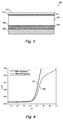
- Figure 1 a illustrates a material structure for a solar cell.
- the material structure 100 comprises a light absorbing layer 102, a metal layer 104 and a graphene layer 106 that is arranged between the light absorbing layer 102 and the metal layer 104 such that the graphene layer 106 forms an electrical interface between the light absorbing layer 102 and the metal layer 104.
- the light absorbing layer 102 comprises Cu(In, Ga)Se 2 , also referred to as CIGS.
- the CIGS light absorbing layer 102 has a higher absorption coefficient than e.g. crystalline silicon, and therefore a lower thickness of the light absorbing layer 102 is needed to collect and absorb the same amount of photons as compared to silicon based solar cells.
- the metal layer 104 comprises copper, Cu.
- the increased reflectivity provided by the Cu metal layer 104 as may be seen in the later discussion relating to figure 1b increase the amount of light on the material structure 100 that may be absorbed by the light absorbing layer 102.
- the thickness of the light absorbing layer 102 may therefore be further reduced, and thinner and more cost effective solar cells may be provided with respect to solar cells not comprising the material structure 100.
- a metal layer 104 comprising Cu further offers improved performance of the material structure 100. Compared with e.g. molybdenum, Mo, the use of Cu may offer improved electrical conductivity, e.g. four times higher, and improved thermal conductivity.
- the cost of Cu is also lower, e.g.
- one fourth of the cost, and the use of Cu may allow for a more cost effective manufacturing of the material structure 100 as compared to a metal layer that comprises Mo.
- a material structure 100 comprising a lower amount, or none, of Mo may thereby be obtained, and the costs associated with material forming the structure 100 may thereby be reduced.
- the graphene layer 106 protects the metal layer 104, e.g. during fabrication and blocks the diffusion of selenium, Se, from the light absorbing layer 102 to the metal layer 104. This prevents the formation of a selenized, e.g. Cu-Se systems, intermediate layer and eliminates the risks of such an intermediate layer becoming too thick or the metal layer being transformed into a semiconductor. Likewise, the graphene layer 106 may prohibit migration of Cu from the metal layer 104 to the absorbing layer 102, a migration which may otherwise reduce the performance of the material structure 100 when used e.g. in a solar cell. A Cu-Se layer that may be present during e.g.
- the graphene layer 106 may also prohibit, or at least partly prohibit, the formation of such a Cu-Se layer.
- the graphene layer 106 may not necessarily be a monolayer, i.e. comprising only a single layer of carbon atoms.
- the graphene layer 106 may be of a bilayer or multilayer type, i.e. comprising two or more layers of carbon atoms arranged in honeycomb-like patterns in each layer, as long as conformal, or at least substantially conformal, coverage between the metal layer 104 and the light absorbing layer 102 is achieved.
- the stacking of the individual layers for bilayer graphene may be of e.g. A-A or A-B (Bernal) type.
- the stacking of the individual layers for multilayer graphene may be of e.g. A-A-A, A-B-A, i.e. Bernal type, A-B-C, rhombohedral type, or of other stacking types depending on e.g. the number of carbon atom layers in the multilayer graphene.
- the graphene layer 106 is arranged on top of the metal layer 104.
- the graphene layer may preferably be grown using the Cu metal layer 104 as a native substrate for growth.
- the graphene layer 106 may thereby be formed directly on top of the metal layer 104. Preferably this is achieved by the use of chemical vapor deposition, CVD, or plasma-enhanced CVD, PE-CVD, but other known and suitable techniques may also be envisaged.
- Figure 1b shows the results of optical reflection data illustrating benefits of arranging the graphene layer 106 between the light absorbing layer 102 and the metal layer 104.
- the reflection, R ⁇ is shown as a percentage ranging from 0 to 100% for different material structures and for different wavelengths, ⁇ , spanning at least the range of visible light.
- a metal layer comprising bare Cu has higher optical reflection than a metal layer comprising bare Mo (dashed line 124).
- adding the graphene layer 106 on top of the metal layer 104 may further increase the optical reflection capabilities of both Cu (solid line 121) and Mo (dashed line 123), as is also shown in the figure. From the measurement results, it is apparent that the combination of Cu with a graphene layer on top (solid line 121) has the highest optical reflection within most of the range of visible light.
- Figure 2 illustrates a material structure 200 for a solar cell, in which a substrate 208 and a buffer layer 210 are included.
- a typical thickness of the substrate 208 is between 1 - 3 mm, although other thicknesses may also be used.
- the metal layer 204 is arranged on the substrate 208.
- the metal layer preferably comprises Cu, or alternatively Mo, but the inclusion or use of other metals, which have a high optical reflection and that would otherwise selenize under the growth of e.g. a CIGS absorbing layer, is also envisaged.
- the metal layer 204 typically has a thickness between 0.5 - 5 ⁇ m.
- the graphene layer 206 is arranged between the metal layer 204 and the light absorbing layer 202, such that it forms an electrical interface between the latter two layers 202 and 204 and allows current to flow in between.
- the light absorbing layer 202 preferably comprises a CIGS compound semiconductor, p-type, and its thickness is typically a few ⁇ m, e.g. between 1 - 6 ⁇ m.
- the buffer layer 210 is deposited on the light absorbing layer 202, and comprises an n-type CdS material.
- the light absorbing layer 202 and the buffer layer 210 thereby form part of a p-n junction that is arranged to convert light into an electric voltage.
- the buffer layer 210 is not as thick as the light absorbing layer 202, allowing for most of the incoming photons to be absorbed in the light absorbing layer 202.
- the thickness of the buffer layer 210 is typically only fractions of a ⁇ m, e.g. around 0.05 ⁇ m, and the buffer layer 210 may be deposited using e.g. a standard chemical bath deposition, CBD, process or any other suitable technique.
- FIG. 3 illustrates a solar cell 300 in which a material structure comprising a light absorbing layer 302, a metal layer 304 and a graphene layer 306 arranged between the layers 302 and 304 is included.
- the material structure and/or the solar cell 300 further includes a substrate 308 on which the metal layer 304 is arranged and a buffer layer 310 that forms part of a p-n junction in combination with the light absorbing layer 302.
- the buffer layer 310 comprises CdS and further forms part of a stack of layers 314 as illustrated in figure 3 .
- the stack of layers 314 may comprise a transparent conducting layer 312 arranged on top of the buffer layer 310.
- the transparent conducting layer 312 comprises, in the depicted embodiment, an i-ZnO/ZnO:Al material, i.e. a thin, intrinsic zinc oxide layer, i-ZnO, which is capped by a thicker, aluminium, Al, doped ZnO layer.
- the i-ZnO layer is used to protect the CdS buffer layer and the light absorbing layer 302 from sputtering damage while depositing the ZnO:Al layer.
- the Al doped ZnO serves as a transparent conducting oxide that is used to collect and move electrons out of the solar cell 300 while absorbing as little light as possible.
- the solar cell 300 comprises a heterostructure junction formed between the CIGS light absorbing layer 302 and the transparent conducting layer 312 of ZnO, which are separated by the thin buffer layer 310 of CdS and a layer of intrinsic ZnO.
- the CIGS light absorbing layer 302 is doped p-type by intrinsic defects, while the ZnO transparent conducting layer 312 is doped n-type to a much larger extent through the incorporation of Al. This asymmetric doping provides a space-charge region that to a larger extent extends into the CIGS than into the ZnO.
- the absorption of light is thereby designed to predominantly occur in the light absorbing layer 302 than in e.g. the buffer layer 310.
- the thicknesses and band gaps of the light absorbing layer 302, the buffer layer 310 and the transparent conducting layer 312 are chosen such that the light is absorbed predominantly in the light absorbing layer 302.
- the band gap of the CIGS light absorbing layer 302 typically ranges between 1.02 eV for CuInSe 2 to 1.65 for CuGaSe 2 providing increased light absorption, while the larger band gaps for ZnO at 3.2 eV and CdS at 2.4 eV minimizes light absorption in the upper layers 310 and 312 that forms part of the stack of layers 314.
- the doped ZnO also serves as a front contact for the current collection.
- the transparent conducting layer 312 may be formed using e.g. a shunt reducing intrinsic ZnO layer, i-ZnO, followed by subsequent sputtering of Al-doped ZnO, ZnO:Al.
- the stack of layers 314 may further comprise, not shown, e.g. an anti-reflective coating which may be formed by evaporation to improve light absorption of the solar cell, mainly by avoiding interference effects.
- a front contact grid comprising e.g. a nickel/aluminium/nickel, Ni/Al/Ni stack, not shown, may further be deposited by e.g. evaporation.
- the buffer layer 210, 310 may alternatively comprise a material selected from the group consisting of Zn 1-x Sn x O y , In 2 S 3 , Zn(S,O,OH), Zn(S,O), InS x O y, ZnS, ZnS:In 2 S 3 and In x S y
- the transparent conductive layer 312 may, moreover, comprise a material selected from the group consisting of Ga-doped ZnO, SnO 2 :In 2 O 3 , SnO 2 :F, CdO:ln, graphene and carbon nano-tubes.
- the metal layer 104, 204, 304 has preferably been described as comprising Cu. It has also been envisaged that the metal layer 104, 204, 304 comprises Mo.
- figure 4 illustrates current as a function of voltage for two solar cell structures both comprising a CIGS light absorbing layer on top of a contact metal layer made of Mo.
- the first structure, solid line 401 further comprises a graphene layer that forms an electrical interface between the light absorbing layer and the metal layer, and thus implements a material structure for a solar cell in accordance with the present inventive concept described herewithin. More specifically, the graphene layer is arranged on top of the metal layer made of Mo.
- the second structure is a reference structure that has no such graphene layer. From figure 4 it may be deduced that the graphene layer may improve the electrical contact of the metal layer and that a material structure according to the present inventive concept may be beneficial.
- the metal layer 104, 204, 304 also may comprise Al, Ag, Au, W, Cr, Ta, Nb, V, Ti, Mn, ZrN, TiN, Nb:TiO 2 , TiB 2 or combinations thereof. It is, however, preferable to use at least Cu or Mo as these metals e.g. also may serve as a catalyst and/or native substrate for growing the graphene layer 106, 206, 306.
- the light absorbing layer 102, 202, 302 has been described as preferably comprising CIGS.
- the light absorbing layer 102, 202, 302 may alternatively comprise another compound semiconductor material such as Cu(In, Ga)(S, Se) 2 , Cu 2 ZnSn(S, Se) 4 or CdTe.
- the substrate 208, 308 may be a glass material such as soda-lime glass, alkali-aluminosilicate glass, boro-silicate glass or quartz, depending on e.g. the preferred process of growing the graphene layer.
- the substrate 208, 308 may alternatively comprise steel, a metal-foil of e.g. aluminium, a polymer, a plastic or a ceramic.
- the light absorbing layer 102, 202, 302 may comprise a III-V or a II-VI semiconductor material. Hence, the light absorbing layer 102, 202, 302 may in some embodiments for example comprise GaAs and/or InP and/or Si.
- the light absorbing layer 102, 202, 302 may be of a material having a perovskite crystal structure, and/or be formed by a chalcopyrite or a kesterite material.
- the substrate may be a sheet of glass or foil.
- the glass substrate may for example have a dimension of 80 cm x 120 cm.
- the foil may typically be arranged in a roll of a specific width, which may be 1 m in extension.
- the substrate 208, 308 may form the metal layer 104, 204, 304 and vice versa.
Landscapes
- Photovoltaic Devices (AREA)
Priority Applications (2)
| Application Number | Priority Date | Filing Date | Title |
|---|---|---|---|
| EP16190415.6A EP3300122A1 (de) | 2016-09-23 | 2016-09-23 | Materialstruktur für eine solarzelle und solarzelle mit der materialstruktur |
| PCT/EP2017/001138 WO2018054541A1 (en) | 2016-09-23 | 2017-09-25 | Material structure for a solar cell and a solar cell comprising the material structure |
Applications Claiming Priority (1)
| Application Number | Priority Date | Filing Date | Title |
|---|---|---|---|
| EP16190415.6A EP3300122A1 (de) | 2016-09-23 | 2016-09-23 | Materialstruktur für eine solarzelle und solarzelle mit der materialstruktur |
Publications (1)
| Publication Number | Publication Date |
|---|---|
| EP3300122A1 true EP3300122A1 (de) | 2018-03-28 |
Family
ID=56990360
Family Applications (1)
| Application Number | Title | Priority Date | Filing Date |
|---|---|---|---|
| EP16190415.6A Withdrawn EP3300122A1 (de) | 2016-09-23 | 2016-09-23 | Materialstruktur für eine solarzelle und solarzelle mit der materialstruktur |
Country Status (2)
| Country | Link |
|---|---|
| EP (1) | EP3300122A1 (de) |
| WO (1) | WO2018054541A1 (de) |
Cited By (1)
| Publication number | Priority date | Publication date | Assignee | Title |
|---|---|---|---|---|
| CN111682079A (zh) * | 2020-06-01 | 2020-09-18 | 大连理工大学 | 一种中/远红外透明导电材料体系及其制备导电薄膜的方法 |
Families Citing this family (1)
| Publication number | Priority date | Publication date | Assignee | Title |
|---|---|---|---|---|
| CN112310230A (zh) * | 2019-07-31 | 2021-02-02 | 东泰高科装备科技有限公司 | 太阳能电池 |
Citations (3)
| Publication number | Priority date | Publication date | Assignee | Title |
|---|---|---|---|---|
| KR101300790B1 (ko) * | 2012-04-16 | 2013-08-29 | 고려대학교 산학협력단 | 확산방지층을 가지는 CdTe 박막 태양전지 및 이의 제조방법 |
| US20150136215A1 (en) * | 2013-11-21 | 2015-05-21 | Tsmc Solar Ltd. | Solar cell contacts and method of fabricating same |
| CN204497243U (zh) * | 2015-03-27 | 2015-07-22 | 西交利物浦大学 | 基于石墨烯的柔性碲化镉薄膜太阳能电池 |
Family Cites Families (1)
| Publication number | Priority date | Publication date | Assignee | Title |
|---|---|---|---|---|
| KR20120095553A (ko) * | 2011-02-21 | 2012-08-29 | 성균관대학교산학협력단 | 그라핀을 이용하는 전자소자, 태양전지 및 태양전지의 제조방법 |
-
2016
- 2016-09-23 EP EP16190415.6A patent/EP3300122A1/de not_active Withdrawn
-
2017
- 2017-09-25 WO PCT/EP2017/001138 patent/WO2018054541A1/en not_active Ceased
Patent Citations (3)
| Publication number | Priority date | Publication date | Assignee | Title |
|---|---|---|---|---|
| KR101300790B1 (ko) * | 2012-04-16 | 2013-08-29 | 고려대학교 산학협력단 | 확산방지층을 가지는 CdTe 박막 태양전지 및 이의 제조방법 |
| US20150136215A1 (en) * | 2013-11-21 | 2015-05-21 | Tsmc Solar Ltd. | Solar cell contacts and method of fabricating same |
| CN204497243U (zh) * | 2015-03-27 | 2015-07-22 | 西交利物浦大学 | 基于石墨烯的柔性碲化镉薄膜太阳能电池 |
Non-Patent Citations (3)
| Title |
|---|
| HOUSHMAND M ET AL: "Simulation Analysis of Thermal Degradation in Graphene Back Contacted CdTe Ultrathin Films", IEEE TRANSACTIONS ON NANOTECHNOLOGY, IEEE SERVICE CENTER, PISCATAWAY, NJ, US, vol. 14, no. 3, 6 May 2015 (2015-05-06), pages 493 - 496, XP011580345, ISSN: 1536-125X, [retrieved on 20150506], DOI: 10.1109/TNANO.2015.2408878 * |
| JUN LIANG ET AL: "Novel Cu Nanowires/Graphene as the Back Contact for CdTe Solar Cells", ADVANCED FUNCTIONAL MATERIALS, WILEY - V C H VERLAG GMBH & CO. KGAA, DE, vol. 22, no. 6, 21 March 2012 (2012-03-21), pages 1267 - 1271, XP001573646, ISSN: 1616-301X, [retrieved on 20120119], DOI: 10.1002/ADFM.201102809 * |
| SCOTT RYAN P ET AL: "Reducing the life cycle environmental impacts of kesterite solar photovoltaics: comparing carbon and molybdenum back contact options", THE INTERNATIONAL JOURNAL OF LIFE CYCLE ASSESSMENT, BERLIN ; HEIDELBERG : SPRINGER, 1996-BIS 2007: LANDSBERG : ECOMED PUBL, DE, vol. 21, no. 1, 2 November 2015 (2015-11-02), pages 29 - 43, XP035938597, ISSN: 0948-3349, [retrieved on 20151102], DOI: 10.1007/S11367-015-0978-4 * |
Cited By (2)
| Publication number | Priority date | Publication date | Assignee | Title |
|---|---|---|---|---|
| CN111682079A (zh) * | 2020-06-01 | 2020-09-18 | 大连理工大学 | 一种中/远红外透明导电材料体系及其制备导电薄膜的方法 |
| CN111682079B (zh) * | 2020-06-01 | 2021-12-14 | 大连理工大学 | 一种中/远红外透明导电材料体系及其制备导电薄膜的方法 |
Also Published As
| Publication number | Publication date |
|---|---|
| WO2018054541A1 (en) | 2018-03-29 |
Similar Documents
| Publication | Publication Date | Title |
|---|---|---|
| JP6689456B2 (ja) | 透明トンネル接合を有する光起電力デバイス | |
| US9972741B2 (en) | Methods of forming thin-film photovoltaic devices with discontinuous passivation layers | |
| US20090020149A1 (en) | Hybrid Multi-Junction Photovoltaic Cells And Associated Methods | |
| CN102299158B (zh) | 单片集成太阳能模块和制造方法 | |
| US20120318352A1 (en) | Photovoltaic device with reflection enhancing layer | |
| JP5520597B2 (ja) | フォトダイオードの製造方法 | |
| US20130104985A1 (en) | Photovoltaic device with mangenese and tellurium interlayer | |
| KR101154786B1 (ko) | 태양전지 및 이의 제조방법 | |
| US20120192923A1 (en) | Photovoltaic device | |
| EP2426731A2 (de) | Vorrichtung zur solarstromerzeugung sowie verfahren zu ihrer herstellung | |
| US20130029450A1 (en) | Method for manufacturing solar cell | |
| KR20130111815A (ko) | 태양전지 및 이의 제조방법 | |
| JP2007335625A (ja) | 太陽電池 | |
| EP3300122A1 (de) | Materialstruktur für eine solarzelle und solarzelle mit der materialstruktur | |
| KR101327126B1 (ko) | 태양전지 및 이를 이용한 태양전지 모듈 | |
| EP3903352B1 (de) | Photovoltaikvorrichtung und verfahren zur herstellung davon | |
| JP2011023520A (ja) | p型半導体膜及び太陽電池 | |
| KR101349484B1 (ko) | 태양전지 모듈 및 이의 제조방법 | |
| JP2017059656A (ja) | 光電変換素子および太陽電池 | |
| EP2733747A2 (de) | Solarzelle | |
| US20140053903A1 (en) | Photoelectric conversion element and solar cell | |
| US10304982B2 (en) | Solar cell module | |
| US9570636B2 (en) | Solar cell and method of fabricating the same | |
| US20120318337A1 (en) | Solar Cell | |
| KR20150115363A (ko) | Ci(g)s 광흡수층을 구비하는 태양전지의 제조 방법 |
Legal Events
| Date | Code | Title | Description |
|---|---|---|---|
| PUAI | Public reference made under article 153(3) epc to a published international application that has entered the european phase |
Free format text: ORIGINAL CODE: 0009012 |
|
| STAA | Information on the status of an ep patent application or granted ep patent |
Free format text: STATUS: THE APPLICATION HAS BEEN PUBLISHED |
|
| AK | Designated contracting states |
Kind code of ref document: A1 Designated state(s): AL AT BE BG CH CY CZ DE DK EE ES FI FR GB GR HR HU IE IS IT LI LT LU LV MC MK MT NL NO PL PT RO RS SE SI SK SM TR |
|
| AX | Request for extension of the european patent |
Extension state: BA ME |
|
| STAA | Information on the status of an ep patent application or granted ep patent |
Free format text: STATUS: THE APPLICATION IS DEEMED TO BE WITHDRAWN |
|
| 18D | Application deemed to be withdrawn |
Effective date: 20180929 |