EP2736072A1 - Superverbindungs-halbleitervorrichtung - Google Patents
Superverbindungs-halbleitervorrichtung Download PDFInfo
- Publication number
- EP2736072A1 EP2736072A1 EP12818128.6A EP12818128A EP2736072A1 EP 2736072 A1 EP2736072 A1 EP 2736072A1 EP 12818128 A EP12818128 A EP 12818128A EP 2736072 A1 EP2736072 A1 EP 2736072A1
- Authority
- EP
- European Patent Office
- Prior art keywords
- region
- layer
- conductivity
- parallel
- type semiconductor
- Prior art date
- Legal status (The legal status is an assumption and is not a legal conclusion. Google has not performed a legal analysis and makes no representation as to the accuracy of the status listed.)
- Granted
Links
Images



Classifications
-
- H—ELECTRICITY
- H10—SEMICONDUCTOR DEVICES; ELECTRIC SOLID-STATE DEVICES NOT OTHERWISE PROVIDED FOR
- H10D—INORGANIC ELECTRIC SEMICONDUCTOR DEVICES
- H10D84/00—Integrated devices formed in or on semiconductor substrates that comprise only semiconducting layers, e.g. on Si wafers or on GaAs-on-Si wafers
- H10D84/101—Integrated devices comprising main components and built-in components, e.g. IGBT having built-in freewheel diode
- H10D84/141—VDMOS having built-in components
- H10D84/143—VDMOS having built-in components the built-in components being PN junction diodes
-
- H—ELECTRICITY
- H10—SEMICONDUCTOR DEVICES; ELECTRIC SOLID-STATE DEVICES NOT OTHERWISE PROVIDED FOR
- H10D—INORGANIC ELECTRIC SEMICONDUCTOR DEVICES
- H10D62/00—Semiconductor bodies, or regions thereof, of devices having potential barriers
- H10D62/10—Shapes, relative sizes or dispositions of the regions of the semiconductor bodies; Shapes of the semiconductor bodies
- H10D62/102—Constructional design considerations for preventing surface leakage or controlling electric field concentration
- H10D62/103—Constructional design considerations for preventing surface leakage or controlling electric field concentration for increasing or controlling the breakdown voltage of reverse-biased devices
- H10D62/105—Constructional design considerations for preventing surface leakage or controlling electric field concentration for increasing or controlling the breakdown voltage of reverse-biased devices by having particular doping profiles, shapes or arrangements of PN junctions; by having supplementary regions, e.g. junction termination extension [JTE]
- H10D62/109—Reduced surface field [RESURF] PN junction structures
- H10D62/111—Multiple RESURF structures, e.g. double RESURF or 3D-RESURF structures
-
- H—ELECTRICITY
- H10—SEMICONDUCTOR DEVICES; ELECTRIC SOLID-STATE DEVICES NOT OTHERWISE PROVIDED FOR
- H10D—INORGANIC ELECTRIC SEMICONDUCTOR DEVICES
- H10D84/00—Integrated devices formed in or on semiconductor substrates that comprise only semiconducting layers, e.g. on Si wafers or on GaAs-on-Si wafers
- H10D84/01—Manufacture or treatment
- H10D84/0123—Integrating together multiple components covered by H10D12/00 or H10D30/00, e.g. integrating multiple IGBTs
- H10D84/0126—Integrating together multiple components covered by H10D12/00 or H10D30/00, e.g. integrating multiple IGBTs the components including insulated gates, e.g. IGFETs
- H10D84/016—Integrating together multiple components covered by H10D12/00 or H10D30/00, e.g. integrating multiple IGBTs the components including insulated gates, e.g. IGFETs the components including vertical IGFETs
-
- H—ELECTRICITY
- H10—SEMICONDUCTOR DEVICES; ELECTRIC SOLID-STATE DEVICES NOT OTHERWISE PROVIDED FOR
- H10D—INORGANIC ELECTRIC SEMICONDUCTOR DEVICES
- H10D84/00—Integrated devices formed in or on semiconductor substrates that comprise only semiconducting layers, e.g. on Si wafers or on GaAs-on-Si wafers
- H10D84/01—Manufacture or treatment
- H10D84/02—Manufacture or treatment characterised by using material-based technologies
- H10D84/03—Manufacture or treatment characterised by using material-based technologies using Group IV technology, e.g. silicon technology or silicon-carbide [SiC] technology
- H10D84/038—Manufacture or treatment characterised by using material-based technologies using Group IV technology, e.g. silicon technology or silicon-carbide [SiC] technology using silicon technology, e.g. SiGe
-
- H—ELECTRICITY
- H10—SEMICONDUCTOR DEVICES; ELECTRIC SOLID-STATE DEVICES NOT OTHERWISE PROVIDED FOR
- H10D—INORGANIC ELECTRIC SEMICONDUCTOR DEVICES
- H10D84/00—Integrated devices formed in or on semiconductor substrates that comprise only semiconducting layers, e.g. on Si wafers or on GaAs-on-Si wafers
- H10D84/80—Integrated devices formed in or on semiconductor substrates that comprise only semiconducting layers, e.g. on Si wafers or on GaAs-on-Si wafers characterised by the integration of at least one component covered by groups H10D12/00 or H10D30/00, e.g. integration of IGFETs
- H10D84/811—Combinations of field-effect devices and one or more diodes, capacitors or resistors
-
- H—ELECTRICITY
- H10—SEMICONDUCTOR DEVICES; ELECTRIC SOLID-STATE DEVICES NOT OTHERWISE PROVIDED FOR
- H10W—GENERIC PACKAGES, INTERCONNECTIONS, CONNECTORS OR OTHER CONSTRUCTIONAL DETAILS OF DEVICES COVERED BY CLASS H10
- H10W40/00—Arrangements for thermal protection or thermal control
-
- H—ELECTRICITY
- H10—SEMICONDUCTOR DEVICES; ELECTRIC SOLID-STATE DEVICES NOT OTHERWISE PROVIDED FOR
- H10D—INORGANIC ELECTRIC SEMICONDUCTOR DEVICES
- H10D62/00—Semiconductor bodies, or regions thereof, of devices having potential barriers
- H10D62/10—Shapes, relative sizes or dispositions of the regions of the semiconductor bodies; Shapes of the semiconductor bodies
- H10D62/124—Shapes, relative sizes or dispositions of the regions of semiconductor bodies or of junctions between the regions
- H10D62/126—Top-view geometrical layouts of the regions or the junctions
- H10D62/127—Top-view geometrical layouts of the regions or the junctions of cellular field-effect devices, e.g. multicellular DMOS transistors or IGBTs
-
- H—ELECTRICITY
- H10—SEMICONDUCTOR DEVICES; ELECTRIC SOLID-STATE DEVICES NOT OTHERWISE PROVIDED FOR
- H10D—INORGANIC ELECTRIC SEMICONDUCTOR DEVICES
- H10D62/00—Semiconductor bodies, or regions thereof, of devices having potential barriers
- H10D62/10—Shapes, relative sizes or dispositions of the regions of the semiconductor bodies; Shapes of the semiconductor bodies
- H10D62/17—Semiconductor regions connected to electrodes not carrying current to be rectified, amplified or switched, e.g. channel regions
- H10D62/393—Body regions of DMOS transistors or IGBTs
Definitions
- the present invention relates to a superjunction semiconductor device having a superjunction structure, and more particularly, to a superjunction semiconductor device including a temperature detecting device.
- a method of detecting the temperature of the semiconductor device As a method of detecting the temperature of the semiconductor device, a method has been known which uses a diode as a temperature detecting device.
- the temperature detecting method detects a potential difference between both terminals of the diode, that is, the forward voltage drop (hereinafter, simply referred to as a forward voltage (VF)) when a forward current flows from a constant current source to the diode which is used as the temperature detecting device.
- VF forward voltage
- the diode has the forward voltage-temperature characteristics in which the forward voltage is linearly changed when the temperature (junction temperature) of the device is changed. Therefore, when the forward voltage of the diode is detected, it is possible to calculate the junction temperature of the device from the detected forward voltage (VF).
- the gate voltage of the device When the detected junction temperature is higher than the allowable temperature, the gate voltage of the device is reduced to limit the operating current, thereby protecting the device from thermal breakdown.
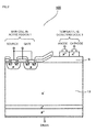
- FIG. 2 is a cross-sectional view illustrating a main portion of the structure of the MOS semiconductor device including the temperature detecting device according to the related art.
- Fig. 2 is a cross-sectional view illustrating the end of a MOS semiconductor device 100.
- the MOS semiconductor device 100 has been known with a temperature detection structure, which is a diode (in Fig. 2 , a temperature detecting diode) 3 provided above the surface of a portion of an n - drift layer 12 in an active region 1, with an insulating film 5 interposed therebetween (for example, see the following Patent Document 1).
- the SJ structure has a parallel structure (hereinafter, referred to as a parallel pn layer) in which p-type regions and n-type regions which extend in a direction perpendicular to the main surface of a substrate and have a small width in a direction parallel to the main surface of the substrate are alternately arranged in an n - drift layer in the direction parallel to the main surface of the substrate.
- the invention has been made in view of the above-mentioned problems of the related art and an object of the invention is to provide a superjunction semiconductor device capable of preventing thermal breakdown and a reduction in breakdown voltage.
- a superjunction semiconductor device includes a drift layer serving as a parallel pn layer in which a first-conductivity-type semiconductor region and a second-conductivity-type semiconductor region extending in a direction perpendicular to a main surface of a first-conductivity-type semiconductor substrate with a high impurity concentration are alternately arranged at a predetermined pitch in a direction parallel to the main surface of the semiconductor substrate so as to be adjacent to each other.
- a current flows to the first-conductivity-type semiconductor region in an on-state and the parallel pn layer is depleted in an off-state to sustain a reverse blocking voltage.
- the superjunction semiconductor device has the following characteristics.
- the superjunction semiconductor device includes an active region that serves as a main current path.
- a temperature detection region in which a pitch between the first-conductivity-type semiconductor region and the second-conductivity-type semiconductor region of the parallel pn layer is less than the predetermined pitch is provided in the active region.
- a first-conductivity-type semiconductor layer is provided above a surface of the parallel pn layer in the temperature detection region with an insulating film interposed therebetween.
- a second-conductivity-type semiconductor layer is provided above the surface of the parallel pn layer in the temperature detection region with the insulating film interposed therebetween and is arranged so as to come into contact with the first-conductivity-type semiconductor layer to form a pn junction.
- a temperature detecting device is provided which is a semiconductor layer including the first-conductivity-type semiconductor layer and the second-conductivity-type semiconductor layer.
- the active region may include an insulated gate structure, and the insulating film provided on the surface of the parallel pn layer in the temperature detection region may be thicker than a gate insulating film forming the insulated gate structure.
- the superjunction semiconductor device may further include an edge termination region that is arranged in the outer circumference of the active region so as to surround the active region and holds a breakdown voltage.
- the insulating film provided on the surface of the parallel pn layer in the temperature detection region may have the same thickness as a field insulating film which protects a surface of the edge termination region.
- a plane pattern of the parallel pn layer in the temperature detection region may have a stripe shape which extends in a direction perpendicular to a direction in which the first-conductivity-type semiconductor region and the second-conductivity-type semiconductor region are arranged.
- a plane pattern of the parallel pn layer in the active region may have the stripe shape which extends in the direction perpendicular to the direction in which the first-conductivity-type semiconductor region and the second-conductivity-type semiconductor region are arranged, and the stripe-shaped plane pattern of the parallel pn layer in the temperature detection region may be parallel or perpendicular to the stripe-shaped plane pattern of the parallel pn layer in the active region.
- the parallel pn layer in the temperature detection region may have a plane pattern in which the second-conductivity-type semiconductor regions are arranged in a matrix in the first-conductivity-type semiconductor region.
- the temperature detecting device may be made of polysilicon.
- the fine SJ cell with a pitch less than that of the main SJ cell is provided as the drift layer below the temperature detecting device in the temperature detection region, with the insulating film interposed therebetween. Therefore, it is possible to obtain a superjunction semiconductor device including a temperature detecting device which can prevent a reduction in breakdown voltage.
- the superjunction semiconductor device can include the temperature detecting device, it is possible to rapidly detect the temperature of a device, apply the detected temperature to a current, and protect the device from thermal breakdown.
- the superjunction semiconductor device of the invention it is possible to provide a superjunction semiconductor device capable of preventing thermal breakdown and a reduction in breakdown voltage.
- Fig. 1 is a cross-sectional view illustrating the structure of the superjunction semiconductor device according to the first embodiment of the invention.
- Fig. 3 is a plan view illustrating the structure of the superjunction semiconductor device according to the first embodiment of the invention.
- Fig. 1 is a cross-sectional view cut along the line A-A' of Fig. 3 .
- Figs. 1 and 3 the same components as those in Fig. 2 are denoted by the same reference numerals.
- the SJ-MOSFET 200 includes an active region 1 in which a MOS gate structure 10 is provided and a temperature detection region 4 in which the temperature detecting device (hereinafter, referred to as a temperature detecting diode 3), which is a diode 3, is provided, and the active region 1 and the temperature detection region 4 are provided on the same n + semiconductor substrate 6.
- a temperature detecting diode 3 the temperature detecting device
- a drift layer 12 is a parallel pn layer (SJ cell) in which n-type regions (hereinafter, referred to as n drift regions) and p-type regions (hereinafter, referred to as p partition regions) with high impurity concentration are alternately arranged.
- Main SJ cells 13 are provided in a portion of the drift layer 12 below the MOS gate structure 10 in the active region 1.
- the temperature detection region 4 is provided in the active region 1.
- fine SJ cells 131 are provided at a pitch less than the pitch of the main SJ cells 13 in a portion of the drift layer 12 which is below the temperature detecting diode 3 with an insulating film 5 interposed therebetween.
- FIG. 3 is a plan view illustrating the entire SJ-MOSFET 200 including the temperature detecting diode 3 according to the first embodiment of the invention.
- the MOS gate structure 10 and a metal film (except for a gate electrode pad) and an insulating film on the surface of the parallel pn layer are not illustrated in order to clarify the plane pattern of the parallel pn layer (the main SJ cells 13 and the fine SJ cells 131) of the SJ-MOSFET 200.
- the SJ-MOSFET 200 includes the n + semiconductor substrate 6 with low resistance (high impurity concentration) and the parallel pn layer (the main SJ cells 13 and the fine SJ cells 131) which is formed on the surface of the n + semiconductor substrate 6.
- the main SJ cells 13 are formed in the active region 1 and the fine SJ cells 131 are formed in the temperature detection region 4.
- the n + semiconductor substrate 6 with low resistance functions as an n + drain region and a metal electrode formed on the backside surface of the n + drain region functions as a drain electrode 7.
- a solderable laminated metal film such as a titanium (Ti)-nickel (Ni)-gold (Au) film, is formed as the drain electrode 7 by, for example, a sputtering method or a vapor deposition method.
- the SJ structure it is possible to reduce an on voltage and increase a breakdown voltage by setting the width of regions on both sides of each pn junction between n drift regions 13b and 131b and p partition regions 13a and 131a with high impurity concentration in a direction in which the regions are arranged (hereinafter, simply referred to as a width) such that a depletion layer is rapidly spread from each pn junction to the regions on both sides of the pn junction and the regions on both sides of the pn junction are fully depleted at a low voltage when the semiconductor device is turned off.
- the invention is characterized in that the pitch of the main SJ cells 13 is different from that of the fine SJ cells 131. That is, the pitches of the p partition regions and the n drift regions forming each cell are different in the main SJ cell 13 and the fine SJ cell 131. Specifically, the width of the p partition region 131a and the n drift region 131b in the fine SJ cell 131 is less than that of the p partition region 13a and the n drift region 13b in the main SJ cell 13. The reason why the pitch of each region in the fine SJ cell 131 is less than that of each region in the main SJ cell 13 is to prevent a reduction in breakdown voltage.
- the n drift region 131b and the p partition region 131a of the parallel pn layer in the temperature detection region 4 have the same width or the same arrangement pitch as the n drift region 13b and the p partition region 13a of the parallel pn layer in the active region 1.
- the insulating film 5 which extends to a surface of the parallel pn layer opposite to the n + semiconductor substrate 6 and comes into contact with the surface is provided between the temperature detecting diode 3 and the parallel pn layer, a portion (the uppermost portion) of the parallel pn layer which comes into contact with the insulating film 5 is not fully depleted. As a result, the electric field is likely to be concentrated on the portion which is not depleted and the breakdown voltage is reduced. For this reason, the fine SJ cells 131 are provided in the above-mentioned structure.
- the main SJ cell 13 includes the n drift region 13b and the p partition region 13a which are arranged adjacent to each other in a direction parallel to the main surface of the n + semiconductor substrate 6.
- the fine SJ cell 131 includes the n drift region 131b and the p partition region 131a which are arranged adjacent to each other in the direction parallel to the main surface of the n + semiconductor substrate 6.
- the n drift regions 13b and 131b and the p partition regions 13a and 131a have a layer shape or a columnar shape which has a small width and extends in a direction perpendicular to the main surface of the n + semiconductor substrate 6. As illustrated in Fig.
- the plane pattern of the n drift region 13b and the p partition region 13a in the active region 1 has, for example, a stripe shape which extends in a direction perpendicular to the direction in which the drift region 13b and the p partition region 13a are arranged.
- the plane pattern of the n drift region 131b and the p partition region 131a in the temperature detection region 4 also has a stripe shape which extends in a direction perpendicular to the direction in which the n drift region 131b and the p partition region 131a are arranged.
- the n drift region 131b and the p partition region 131a in the temperature detection region 4 are parallel to the n drift region 13b and the p partition region 13a in the active region 1. It is preferable that the pitch of the stripe-shaped plane pattern of the n drift region 131b and the p partition region 131a be half the pitch of the stripe-shaped plane pattern of the n drift region 13b and the p partition region 13a in the active region 1. The reason is as follows. The mutual diffusion between the n drift region 131b and the p partition region 131a in the temperature detection region 4 is large and impurity concentration is compensated, which makes it possible to reduce the impurity concentration of both regions. As a result, the depletion layer is easily spread.
- the directions in which the stripe-shaped plane pattern of each parallel pn layer extends in the active region 1 and the temperature detection region 4 are parallel to each other.
- a white rectangular region which is illustrated on the upper side of the temperature detection region 4 in the active region 1 is a gate electrode pad portion.
- an edge termination region 2 which reduces the electric field of the end of the active region 1 to hold the breakdown voltage is provided so as to surround the outer circumference of the active region 1. Since the edge termination region 2 is the same as the edge termination region of the MOSFET according to the related art, the detailed description thereof will not be made.
- a p base region 14 is provided in a surface layer of each p partition region 13a opposite to the n + semiconductor substrate 6.
- An n + source region 15 and a high-concentration p + contact region 14a are provided in the p base region 14 so as to be exposed from the surface of the parallel pn layer opposite to the n + semiconductor substrate 6.
- a gate electrode 16, which is a polysilicon film, is provided above a portion of the p base region 14 interposed between the n + source region 15 and the n drift region 13b, with a gate insulating film 5a interposed therebetween.
- the gate electrode 16 is covered with an interlayer insulating film 8 to be electrically insulated from the source electrode 17 which covers the interlayer insulating film 8.
- the temperature detecting diode 3 is formed on the surface of the fine SJ cell 131 opposite to the n + semiconductor substrate 6 with the thick insulating film 5 interposed therebetween.
- the temperature detecting diode 3 includes a p + anode region and an n + cathode region which are laminated so as to come into contact with the surface of the insulating film 5 and a pn junction is formed between the two regions.
- an anode electrode is provided on the surface of the p + anode region and a cathode electrode is provided on the surface of the n + cathode region.
- the insulating film 5 be as thick as possible in order to prevent the interference between the temperature detecting diode 3 and the fine SJ cell 131.
- an oxide film that is formed at the same time as a field oxide film formed as a protective film on the surface of the drift layer of the edge termination region 2 (not illustrated in Fig. 1 ) be used as the insulating film 5.
- the insulating film 5 has the same thickness as the thick field oxide film.
- the temperature detecting diode 3 is formed while being electrically insulated from the fine SJ cell 131 by the insulating film 5.
- the temperature detecting diode 3 is electrically insulated from the fine SJ cell 131, there is a concern that depletion will be insufficient since, for example, the field plate effect of the edge termination region 2 affects the parallel pn layer (fine SJ cell 131) immediately below the insulating film 5.
- the pitch between the fine SJ cells 131 below the temperature detecting diode 3 in the temperature detection region 4 is less than the pitch between the main SJ cells 13 in the active region 1, the effect of preventing reduction in the breakdown voltage is obtained.
- the depletion layer is more likely to be spread by an off-state voltage than in the main SJ cell 13 in the active region 1. Therefore, in the SJ-MOSFET 200 according to the first embodiment, a reduction in the breakdown voltage which has occurred in the SJ-MOSFET according to the related art is prevented and a high breakdown voltage is obtained.
- the p base region 14 is not formed in the upper part of the fine SJ cell 131 in the temperature detection region 4, unlike the main SJ cell 13.
- the length of the fine SJ cell 131 in the direction perpendicular to the main surface of the n + semiconductor substrate 6 is more than that of the main SJ cell 13 by a value corresponding to the p base region 14. Therefore, it is expected to obtain a higher breakdown voltage than that in the active region 1.
- the temperature detection region 4 may not be provided at the center of the active region 1. That is, the temperature detection region 4 may be provided at any position of the active region 1.
- Fig. 4 is a plan view illustrating the structure of a superjunction semiconductor device according to a second embodiment of the invention.
- An SJ-MOSFET 300 according to the second embodiment differs from the SJ-MOSFET 200 according to the first embodiment in that the stripe-shaped plane pattern of the temperature detection region 4 is perpendicular to the stripe-shaped plane pattern of the active region 1.
- a fine SJ cell 141 in the temperature detection region 4 is similar to the fine SJ cell illustrated in Fig. 3 in that it has a stripe-shaped plane pattern which extends in a direction perpendicular to the direction in which an n drift region 141b and a p partition region 141a are arranged.
- the fine SJ cell 141 differs from the fine SJ cell illustrated in Fig. 3 in that the direction in which the stripe of the plane pattern of the fine SJ cell 141 extends is perpendicular to the direction in which the stripe of the plane pattern of the main SJ cell 13 in the active region 1 extends.
- the same effect as that in the first embodiment is obtained.
- the stripe-shaped plane patterns of the fine SJ cell 141 and the main SJ cell 13 are perpendicular to each other, flexibility in the design of the pitch between the SJ cells is improved. Therefore, it is easy to reduce the pitch and increase the breakdown voltage.
- Fig. 5 is a plan view illustrating the structure of a superjunction semiconductor device according to a third embodiment of the invention.
- An SJ-MOSFET 400 according to the third embodiment differs from the SJ-MOSFETs 200 and 300 according to the first and second embodiments in that fine SJ cells 151 in the temperature detection region 4 have a lattice-shaped plane pattern.
- the lattice-shaped plane pattern means a plane pattern in which p partition regions 151a having a rectangular shape in a plan view are arranged in a matrix in an n drift region 151b.
- the pitch of the lattice-shaped plane pattern of the fine SJ cells 151 is less than that of the stripe-shaped plane pattern of the main SJ cells 13. Therefore, the same effect as that in the first embodiment is obtained.
- the drift layer including the fine SJ cells which are arranged at a pitch less than that of the main SJ cells is provided below the temperature detecting diode, with the insulating film interposed therebetween.
- the superjunction semiconductor device can include the temperature detecting device, it is possible to rapidly detect the device temperature, apply the detected device temperature to the on current, and protect the device from thermal breakdown. Therefore, it is possible to provide a superjunction semiconductor device capable of preventing thermal breakdown and a reduction in the breakdown voltage.
- the SJ-MOSFET has been described as an example, but the invention is not limited to the above-described embodiments.
- the invention can be applied to various superjunction semiconductor devices including the temperature detecting diode.
- the first-conductivity-type is an n type and the second-conductivity-type is a p type.
- the first-conductivity-type may be a p type and the second-conductivity-type may be an n type. In this case, the same effect as described above is obtained.
- the superjunction semiconductor device according to the invention is effective for a power semiconductor device which is used in, for example, a switching device that is repeatedly turned on and off.
Landscapes
- Metal-Oxide And Bipolar Metal-Oxide Semiconductor Integrated Circuits (AREA)
- Semiconductor Integrated Circuits (AREA)
- Chemical & Material Sciences (AREA)
- Composite Materials (AREA)
Applications Claiming Priority (2)
| Application Number | Priority Date | Filing Date | Title |
|---|---|---|---|
| JP2011160756 | 2011-07-22 | ||
| PCT/JP2012/064007 WO2013015014A1 (ja) | 2011-07-22 | 2012-05-30 | 超接合半導体装置 |
Publications (3)
| Publication Number | Publication Date |
|---|---|
| EP2736072A1 true EP2736072A1 (de) | 2014-05-28 |
| EP2736072A4 EP2736072A4 (de) | 2015-02-25 |
| EP2736072B1 EP2736072B1 (de) | 2017-01-11 |
Family
ID=47600874
Family Applications (1)
| Application Number | Title | Priority Date | Filing Date |
|---|---|---|---|
| EP12818128.6A Not-in-force EP2736072B1 (de) | 2011-07-22 | 2012-05-30 | Superjunction-halbleitervorrichtung |
Country Status (6)
| Country | Link |
|---|---|
| US (1) | US20140061644A1 (de) |
| EP (1) | EP2736072B1 (de) |
| JP (1) | JP5720788B2 (de) |
| CN (1) | CN103650141B (de) |
| TW (1) | TWI567975B (de) |
| WO (1) | WO2013015014A1 (de) |
Families Citing this family (22)
| Publication number | Priority date | Publication date | Assignee | Title |
|---|---|---|---|---|
| US9614043B2 (en) | 2012-02-09 | 2017-04-04 | Vishay-Siliconix | MOSFET termination trench |
| US9842911B2 (en) | 2012-05-30 | 2017-12-12 | Vishay-Siliconix | Adaptive charge balanced edge termination |
| JP6197294B2 (ja) * | 2013-01-16 | 2017-09-20 | 富士電機株式会社 | 半導体素子 |
| US9891640B2 (en) | 2013-06-14 | 2018-02-13 | Infineon Technologies Ag | Sensing element for semiconductor |
| US9887259B2 (en) | 2014-06-23 | 2018-02-06 | Vishay-Siliconix | Modulated super junction power MOSFET devices |
| WO2016002963A1 (ja) | 2014-07-04 | 2016-01-07 | 富士電機株式会社 | 半導体装置 |
| KR102098996B1 (ko) | 2014-08-19 | 2020-04-08 | 비쉐이-실리코닉스 | 초접합 금속 산화물 반도체 전계 효과 트랜지스터 |
| JP6503202B2 (ja) * | 2015-03-12 | 2019-04-17 | エイブリック株式会社 | 半導体装置 |
| US9881997B2 (en) * | 2015-04-02 | 2018-01-30 | Fuji Electric Co., Ltd. | Semiconductor device and manufacturing method of semiconductor device |
| JP6512025B2 (ja) | 2015-08-11 | 2019-05-15 | 富士電機株式会社 | 半導体素子及び半導体素子の製造方法 |
| CN106560909B (zh) * | 2015-09-30 | 2019-05-28 | 中芯国际集成电路制造(上海)有限公司 | 测试结构及其形成方法、测试方法 |
| JP6805620B2 (ja) * | 2016-08-10 | 2020-12-23 | 富士電機株式会社 | 半導体装置 |
| JP6747195B2 (ja) * | 2016-09-08 | 2020-08-26 | 富士電機株式会社 | 半導体装置および半導体装置の製造方法 |
| JP6963453B2 (ja) * | 2017-10-02 | 2021-11-10 | 京セラ株式会社 | チップ型圧電デバイス及びその製造方法 |
| JP7092188B2 (ja) * | 2018-04-19 | 2022-06-28 | 日産自動車株式会社 | 半導体装置及びその製造方法 |
| CN108878305B (zh) * | 2018-06-29 | 2020-09-25 | 上海华虹宏力半导体制造有限公司 | 超结器件的终端结构的耐压验证方法 |
| JP7055087B2 (ja) * | 2018-11-07 | 2022-04-15 | 三菱電機株式会社 | 半導体装置およびその製造方法 |
| JP7080166B2 (ja) * | 2018-12-21 | 2022-06-03 | 三菱電機株式会社 | 半導体装置、および、半導体装置の製造方法 |
| CN113035949A (zh) * | 2019-12-25 | 2021-06-25 | 株洲中车时代半导体有限公司 | Igbt芯片 |
| JP7454454B2 (ja) * | 2020-06-18 | 2024-03-22 | ルネサスエレクトロニクス株式会社 | 半導体装置およびその製造方法 |
| WO2021260851A1 (ja) * | 2020-06-24 | 2021-12-30 | 三菱電機株式会社 | 半導体装置およびその製造方法 |
| CN112349715B (zh) * | 2020-11-05 | 2024-03-26 | 宁波宝芯源功率半导体有限公司 | 具有温度及电压检测功能的功率半导体器件及制作方法 |
Family Cites Families (30)
| Publication number | Priority date | Publication date | Assignee | Title |
|---|---|---|---|---|
| JPH0334360A (ja) * | 1989-06-29 | 1991-02-14 | Nec Corp | 半導体装置 |
| JPH06117942A (ja) | 1992-10-06 | 1994-04-28 | Fuji Electric Co Ltd | 半導体装置 |
| JP3982842B2 (ja) * | 1993-08-18 | 2007-09-26 | 株式会社ルネサステクノロジ | 半導体装置 |
| JP2701824B2 (ja) * | 1996-02-09 | 1998-01-21 | 株式会社デンソー | 半導体装置 |
| JP3911566B2 (ja) * | 1998-01-27 | 2007-05-09 | 富士電機デバイステクノロジー株式会社 | Mos型半導体装置 |
| JP4774580B2 (ja) * | 1999-08-23 | 2011-09-14 | 富士電機株式会社 | 超接合半導体素子 |
| JP4765012B2 (ja) * | 2000-02-09 | 2011-09-07 | 富士電機株式会社 | 半導体装置及びその製造方法 |
| JP3899231B2 (ja) * | 2000-12-18 | 2007-03-28 | 株式会社豊田中央研究所 | 半導体装置 |
| JP2002190575A (ja) * | 2000-12-21 | 2002-07-05 | Toyota Industries Corp | 半導体装置およびその製造方法 |
| JP2002208702A (ja) * | 2001-01-10 | 2002-07-26 | Mitsubishi Electric Corp | パワー半導体装置 |
| JP4140232B2 (ja) * | 2001-12-07 | 2008-08-27 | 株式会社デンソー | 半導体装置 |
| EP1469523B1 (de) * | 2003-04-18 | 2008-12-24 | STMicroelectronics S.r.l. | Elektronisches Bauteil mit Übergang und mit dem Bauteil integriertes Leistungs-Bauelement |
| JP4166627B2 (ja) * | 2003-05-30 | 2008-10-15 | 株式会社デンソー | 半導体装置 |
| US7541643B2 (en) * | 2005-04-07 | 2009-06-02 | Kabushiki Kaisha Toshiba | Semiconductor device |
| JP2006313892A (ja) * | 2005-04-07 | 2006-11-16 | Toshiba Corp | 半導体素子 |
| JP4997715B2 (ja) | 2005-05-18 | 2012-08-08 | 富士電機株式会社 | 半導体装置およびその製造方法 |
| JP4921730B2 (ja) * | 2005-06-20 | 2012-04-25 | 株式会社東芝 | 半導体装置 |
| US8084815B2 (en) * | 2005-06-29 | 2011-12-27 | Fairchild Korea Semiconductor Ltd. | Superjunction semiconductor device |
| DE102007063721B4 (de) * | 2006-03-22 | 2014-05-08 | Denso Corporation | Schaltkreis mit einem Transistor und einer Ansteuerschaltung zur Ansteuerung des Transistors |
| JP2008177328A (ja) * | 2007-01-18 | 2008-07-31 | Denso Corp | 半導体装置およびその製造方法 |
| JP5309497B2 (ja) * | 2007-08-09 | 2013-10-09 | 富士電機株式会社 | 半導体装置 |
| JP5298488B2 (ja) * | 2007-09-28 | 2013-09-25 | 富士電機株式会社 | 半導体装置 |
| US8278731B2 (en) * | 2007-11-20 | 2012-10-02 | Denso Corporation | Semiconductor device having SOI substrate and method for manufacturing the same |
| JP4737255B2 (ja) * | 2007-11-20 | 2011-07-27 | 株式会社デンソー | Soi基板を用いた半導体装置 |
| US8089134B2 (en) * | 2008-02-06 | 2012-01-03 | Fuji Electric Sytems Co., Ltd. | Semiconductor device |
| JP5560538B2 (ja) * | 2008-05-22 | 2014-07-30 | 富士電機株式会社 | 半導体装置の製造方法 |
| US20120273916A1 (en) * | 2011-04-27 | 2012-11-01 | Yedinak Joseph A | Superjunction Structures for Power Devices and Methods of Manufacture |
| JP2011066184A (ja) * | 2009-09-17 | 2011-03-31 | Renesas Electronics Corp | 半導体装置、及びその製造方法 |
| CN102214689B (zh) * | 2010-04-06 | 2012-11-07 | 上海华虹Nec电子有限公司 | 超级结器件的终端保护结构及其制造方法 |
| JP5757101B2 (ja) * | 2011-02-17 | 2015-07-29 | 富士電機株式会社 | 超接合半導体素子 |
-
2012
- 2012-05-30 EP EP12818128.6A patent/EP2736072B1/de not_active Not-in-force
- 2012-05-30 CN CN201280034308.7A patent/CN103650141B/zh not_active Expired - Fee Related
- 2012-05-30 WO PCT/JP2012/064007 patent/WO2013015014A1/ja not_active Ceased
- 2012-05-30 JP JP2013525609A patent/JP5720788B2/ja not_active Expired - Fee Related
- 2012-07-19 TW TW101126043A patent/TWI567975B/zh not_active IP Right Cessation
-
2013
- 2013-11-13 US US14/079,101 patent/US20140061644A1/en not_active Abandoned
Also Published As
| Publication number | Publication date |
|---|---|
| CN103650141B (zh) | 2016-06-29 |
| JPWO2013015014A1 (ja) | 2015-02-23 |
| TW201316506A (zh) | 2013-04-16 |
| TWI567975B (zh) | 2017-01-21 |
| JP5720788B2 (ja) | 2015-05-20 |
| CN103650141A (zh) | 2014-03-19 |
| EP2736072B1 (de) | 2017-01-11 |
| US20140061644A1 (en) | 2014-03-06 |
| EP2736072A4 (de) | 2015-02-25 |
| WO2013015014A1 (ja) | 2013-01-31 |
Similar Documents
| Publication | Publication Date | Title |
|---|---|---|
| EP2736072B1 (de) | Superjunction-halbleitervorrichtung | |
| US20200295129A1 (en) | Superjunction silicon carbide semiconductor device and method of manufacturing superjunction silicon carbide semiconductor device | |
| JP7505217B2 (ja) | 超接合半導体装置および超接合半導体装置の製造方法 | |
| EP2498292B1 (de) | Schottky-Barrierendiode | |
| US8742500B2 (en) | Semiconductor device | |
| US10090417B2 (en) | Silicon carbide semiconductor device and fabrication method of silicon carbide semiconductor device | |
| US20050045892A1 (en) | Semiconductor device and method of manufacturing the same | |
| US20180358431A1 (en) | Power semiconductor device | |
| JP2013149761A (ja) | 半導体装置 | |
| WO2018037701A1 (ja) | 半導体装置 | |
| TW201438241A (zh) | 半導體元件 | |
| US20160308037A1 (en) | Semiconductor device | |
| JP7472059B2 (ja) | 半導体装置 | |
| US20150076521A1 (en) | Vertical high-voltage semiconductor device and fabrication method thereof | |
| JP2024009372A (ja) | 超接合半導体装置 | |
| US9620600B2 (en) | Semiconductor device having termination region with laterally heterogeneous insulating films | |
| JP2017168669A (ja) | 半導体装置 | |
| EP4016641B1 (de) | Halbleiterbauelement und layout für gate-elektroden | |
| JP5735611B2 (ja) | SiC半導体装置 | |
| JP2008294028A (ja) | 半導体装置 | |
| US20160276441A1 (en) | Semiconductor device | |
| JP2009099911A (ja) | 半導体装置 | |
| US20150221641A1 (en) | Semiconductor device | |
| US20150053998A1 (en) | Semiconductor device | |
| US11342435B2 (en) | Wide-gap semiconductor device |
Legal Events
| Date | Code | Title | Description |
|---|---|---|---|
| PUAI | Public reference made under article 153(3) epc to a published international application that has entered the european phase |
Free format text: ORIGINAL CODE: 0009012 |
|
| 17P | Request for examination filed |
Effective date: 20131113 |
|
| AK | Designated contracting states |
Kind code of ref document: A1 Designated state(s): AL AT BE BG CH CY CZ DE DK EE ES FI FR GB GR HR HU IE IS IT LI LT LU LV MC MK MT NL NO PL PT RO RS SE SI SK SM TR |
|
| DAX | Request for extension of the european patent (deleted) | ||
| REG | Reference to a national code |
Ref country code: DE Ref legal event code: R079 Ref document number: 602012027825 Country of ref document: DE Free format text: PREVIOUS MAIN CLASS: H01L0027040000 Ipc: H01L0027060000 |
|
| A4 | Supplementary search report drawn up and despatched |
Effective date: 20150127 |
|
| RIC1 | Information provided on ipc code assigned before grant |
Ipc: H01L 27/06 20060101AFI20150121BHEP Ipc: H01L 29/78 20060101ALI20150121BHEP Ipc: H01L 29/06 20060101ALI20150121BHEP |
|
| 17Q | First examination report despatched |
Effective date: 20151102 |
|
| GRAP | Despatch of communication of intention to grant a patent |
Free format text: ORIGINAL CODE: EPIDOSNIGR1 |
|
| INTG | Intention to grant announced |
Effective date: 20160719 |
|
| GRAS | Grant fee paid |
Free format text: ORIGINAL CODE: EPIDOSNIGR3 |
|
| STAA | Information on the status of an ep patent application or granted ep patent |
Free format text: STATUS: GRANT OF PATENT IS INTENDED |
|
| GRAA | (expected) grant |
Free format text: ORIGINAL CODE: 0009210 |
|
| STAA | Information on the status of an ep patent application or granted ep patent |
Free format text: STATUS: THE PATENT HAS BEEN GRANTED |
|
| AK | Designated contracting states |
Kind code of ref document: B1 Designated state(s): AL AT BE BG CH CY CZ DE DK EE ES FI FR GB GR HR HU IE IS IT LI LT LU LV MC MK MT NL NO PL PT RO RS SE SI SK SM TR |
|
| REG | Reference to a national code |
Ref country code: GB Ref legal event code: FG4D |
|
| RIN1 | Information on inventor provided before grant (corrected) |
Inventor name: CAO, DAWEI Inventor name: ONISHI, YASUHIKO |
|
| REG | Reference to a national code |
Ref country code: CH Ref legal event code: EP |
|
| REG | Reference to a national code |
Ref country code: AT Ref legal event code: REF Ref document number: 861973 Country of ref document: AT Kind code of ref document: T Effective date: 20170115 |
|
| REG | Reference to a national code |
Ref country code: IE Ref legal event code: FG4D |
|
| REG | Reference to a national code |
Ref country code: DE Ref legal event code: R096 Ref document number: 602012027825 Country of ref document: DE |
|
| REG | Reference to a national code |
Ref country code: LT Ref legal event code: MG4D |
|
| REG | Reference to a national code |
Ref country code: NL Ref legal event code: MP Effective date: 20170111 |
|
| REG | Reference to a national code |
Ref country code: AT Ref legal event code: MK05 Ref document number: 861973 Country of ref document: AT Kind code of ref document: T Effective date: 20170111 |
|
| PG25 | Lapsed in a contracting state [announced via postgrant information from national office to epo] |
Ref country code: NL Free format text: LAPSE BECAUSE OF FAILURE TO SUBMIT A TRANSLATION OF THE DESCRIPTION OR TO PAY THE FEE WITHIN THE PRESCRIBED TIME-LIMIT Effective date: 20170111 |
|
| PG25 | Lapsed in a contracting state [announced via postgrant information from national office to epo] |
Ref country code: FI Free format text: LAPSE BECAUSE OF FAILURE TO SUBMIT A TRANSLATION OF THE DESCRIPTION OR TO PAY THE FEE WITHIN THE PRESCRIBED TIME-LIMIT Effective date: 20170111 Ref country code: LT Free format text: LAPSE BECAUSE OF FAILURE TO SUBMIT A TRANSLATION OF THE DESCRIPTION OR TO PAY THE FEE WITHIN THE PRESCRIBED TIME-LIMIT Effective date: 20170111 Ref country code: IS Free format text: LAPSE BECAUSE OF FAILURE TO SUBMIT A TRANSLATION OF THE DESCRIPTION OR TO PAY THE FEE WITHIN THE PRESCRIBED TIME-LIMIT Effective date: 20170511 Ref country code: NO Free format text: LAPSE BECAUSE OF FAILURE TO SUBMIT A TRANSLATION OF THE DESCRIPTION OR TO PAY THE FEE WITHIN THE PRESCRIBED TIME-LIMIT Effective date: 20170411 Ref country code: HR Free format text: LAPSE BECAUSE OF FAILURE TO SUBMIT A TRANSLATION OF THE DESCRIPTION OR TO PAY THE FEE WITHIN THE PRESCRIBED TIME-LIMIT Effective date: 20170111 Ref country code: GR Free format text: LAPSE BECAUSE OF FAILURE TO SUBMIT A TRANSLATION OF THE DESCRIPTION OR TO PAY THE FEE WITHIN THE PRESCRIBED TIME-LIMIT Effective date: 20170412 |
|
| PG25 | Lapsed in a contracting state [announced via postgrant information from national office to epo] |
Ref country code: AT Free format text: LAPSE BECAUSE OF FAILURE TO SUBMIT A TRANSLATION OF THE DESCRIPTION OR TO PAY THE FEE WITHIN THE PRESCRIBED TIME-LIMIT Effective date: 20170111 Ref country code: LV Free format text: LAPSE BECAUSE OF FAILURE TO SUBMIT A TRANSLATION OF THE DESCRIPTION OR TO PAY THE FEE WITHIN THE PRESCRIBED TIME-LIMIT Effective date: 20170111 Ref country code: ES Free format text: LAPSE BECAUSE OF FAILURE TO SUBMIT A TRANSLATION OF THE DESCRIPTION OR TO PAY THE FEE WITHIN THE PRESCRIBED TIME-LIMIT Effective date: 20170111 Ref country code: PT Free format text: LAPSE BECAUSE OF FAILURE TO SUBMIT A TRANSLATION OF THE DESCRIPTION OR TO PAY THE FEE WITHIN THE PRESCRIBED TIME-LIMIT Effective date: 20170511 Ref country code: PL Free format text: LAPSE BECAUSE OF FAILURE TO SUBMIT A TRANSLATION OF THE DESCRIPTION OR TO PAY THE FEE WITHIN THE PRESCRIBED TIME-LIMIT Effective date: 20170111 Ref country code: SE Free format text: LAPSE BECAUSE OF FAILURE TO SUBMIT A TRANSLATION OF THE DESCRIPTION OR TO PAY THE FEE WITHIN THE PRESCRIBED TIME-LIMIT Effective date: 20170111 Ref country code: BG Free format text: LAPSE BECAUSE OF FAILURE TO SUBMIT A TRANSLATION OF THE DESCRIPTION OR TO PAY THE FEE WITHIN THE PRESCRIBED TIME-LIMIT Effective date: 20170411 Ref country code: LU Free format text: LAPSE BECAUSE OF NON-PAYMENT OF DUE FEES Effective date: 20170531 Ref country code: RS Free format text: LAPSE BECAUSE OF FAILURE TO SUBMIT A TRANSLATION OF THE DESCRIPTION OR TO PAY THE FEE WITHIN THE PRESCRIBED TIME-LIMIT Effective date: 20170111 |
|
| REG | Reference to a national code |
Ref country code: DE Ref legal event code: R097 Ref document number: 602012027825 Country of ref document: DE |
|
| PG25 | Lapsed in a contracting state [announced via postgrant information from national office to epo] |
Ref country code: IT Free format text: LAPSE BECAUSE OF FAILURE TO SUBMIT A TRANSLATION OF THE DESCRIPTION OR TO PAY THE FEE WITHIN THE PRESCRIBED TIME-LIMIT Effective date: 20170111 Ref country code: EE Free format text: LAPSE BECAUSE OF FAILURE TO SUBMIT A TRANSLATION OF THE DESCRIPTION OR TO PAY THE FEE WITHIN THE PRESCRIBED TIME-LIMIT Effective date: 20170111 Ref country code: SK Free format text: LAPSE BECAUSE OF FAILURE TO SUBMIT A TRANSLATION OF THE DESCRIPTION OR TO PAY THE FEE WITHIN THE PRESCRIBED TIME-LIMIT Effective date: 20170111 Ref country code: RO Free format text: LAPSE BECAUSE OF FAILURE TO SUBMIT A TRANSLATION OF THE DESCRIPTION OR TO PAY THE FEE WITHIN THE PRESCRIBED TIME-LIMIT Effective date: 20170111 Ref country code: CZ Free format text: LAPSE BECAUSE OF FAILURE TO SUBMIT A TRANSLATION OF THE DESCRIPTION OR TO PAY THE FEE WITHIN THE PRESCRIBED TIME-LIMIT Effective date: 20170111 |
|
| PLBE | No opposition filed within time limit |
Free format text: ORIGINAL CODE: 0009261 |
|
| STAA | Information on the status of an ep patent application or granted ep patent |
Free format text: STATUS: NO OPPOSITION FILED WITHIN TIME LIMIT |
|
| PG25 | Lapsed in a contracting state [announced via postgrant information from national office to epo] |
Ref country code: SM Free format text: LAPSE BECAUSE OF FAILURE TO SUBMIT A TRANSLATION OF THE DESCRIPTION OR TO PAY THE FEE WITHIN THE PRESCRIBED TIME-LIMIT Effective date: 20170111 Ref country code: DK Free format text: LAPSE BECAUSE OF FAILURE TO SUBMIT A TRANSLATION OF THE DESCRIPTION OR TO PAY THE FEE WITHIN THE PRESCRIBED TIME-LIMIT Effective date: 20170111 |
|
| 26N | No opposition filed |
Effective date: 20171012 |
|
| REG | Reference to a national code |
Ref country code: CH Ref legal event code: PL |
|
| GBPC | Gb: european patent ceased through non-payment of renewal fee |
Effective date: 20170530 |
|
| PG25 | Lapsed in a contracting state [announced via postgrant information from national office to epo] |
Ref country code: MC Free format text: LAPSE BECAUSE OF FAILURE TO SUBMIT A TRANSLATION OF THE DESCRIPTION OR TO PAY THE FEE WITHIN THE PRESCRIBED TIME-LIMIT Effective date: 20170111 |
|
| REG | Reference to a national code |
Ref country code: IE Ref legal event code: MM4A |
|
| PG25 | Lapsed in a contracting state [announced via postgrant information from national office to epo] |
Ref country code: CH Free format text: LAPSE BECAUSE OF NON-PAYMENT OF DUE FEES Effective date: 20170531 Ref country code: SI Free format text: LAPSE BECAUSE OF FAILURE TO SUBMIT A TRANSLATION OF THE DESCRIPTION OR TO PAY THE FEE WITHIN THE PRESCRIBED TIME-LIMIT Effective date: 20170111 Ref country code: LI Free format text: LAPSE BECAUSE OF NON-PAYMENT OF DUE FEES Effective date: 20170531 |
|
| REG | Reference to a national code |
Ref country code: FR Ref legal event code: ST Effective date: 20180131 |
|
| PG25 | Lapsed in a contracting state [announced via postgrant information from national office to epo] |
Ref country code: LU Free format text: LAPSE BECAUSE OF NON-PAYMENT OF DUE FEES Effective date: 20170530 |
|
| REG | Reference to a national code |
Ref country code: BE Ref legal event code: MM Effective date: 20170531 |
|
| PG25 | Lapsed in a contracting state [announced via postgrant information from national office to epo] |
Ref country code: IE Free format text: LAPSE BECAUSE OF NON-PAYMENT OF DUE FEES Effective date: 20170530 Ref country code: GB Free format text: LAPSE BECAUSE OF NON-PAYMENT OF DUE FEES Effective date: 20170530 |
|
| PG25 | Lapsed in a contracting state [announced via postgrant information from national office to epo] |
Ref country code: FR Free format text: LAPSE BECAUSE OF NON-PAYMENT OF DUE FEES Effective date: 20170531 |
|
| PG25 | Lapsed in a contracting state [announced via postgrant information from national office to epo] |
Ref country code: BE Free format text: LAPSE BECAUSE OF NON-PAYMENT OF DUE FEES Effective date: 20170531 |
|
| PG25 | Lapsed in a contracting state [announced via postgrant information from national office to epo] |
Ref country code: MT Free format text: LAPSE BECAUSE OF NON-PAYMENT OF DUE FEES Effective date: 20170530 |
|
| PG25 | Lapsed in a contracting state [announced via postgrant information from national office to epo] |
Ref country code: HU Free format text: LAPSE BECAUSE OF FAILURE TO SUBMIT A TRANSLATION OF THE DESCRIPTION OR TO PAY THE FEE WITHIN THE PRESCRIBED TIME-LIMIT; INVALID AB INITIO Effective date: 20120530 |
|
| PGFP | Annual fee paid to national office [announced via postgrant information from national office to epo] |
Ref country code: DE Payment date: 20190514 Year of fee payment: 8 |
|
| PG25 | Lapsed in a contracting state [announced via postgrant information from national office to epo] |
Ref country code: CY Free format text: LAPSE BECAUSE OF NON-PAYMENT OF DUE FEES Effective date: 20170111 |
|
| PG25 | Lapsed in a contracting state [announced via postgrant information from national office to epo] |
Ref country code: MK Free format text: LAPSE BECAUSE OF FAILURE TO SUBMIT A TRANSLATION OF THE DESCRIPTION OR TO PAY THE FEE WITHIN THE PRESCRIBED TIME-LIMIT Effective date: 20170111 |
|
| PG25 | Lapsed in a contracting state [announced via postgrant information from national office to epo] |
Ref country code: TR Free format text: LAPSE BECAUSE OF FAILURE TO SUBMIT A TRANSLATION OF THE DESCRIPTION OR TO PAY THE FEE WITHIN THE PRESCRIBED TIME-LIMIT Effective date: 20170111 |
|
| PG25 | Lapsed in a contracting state [announced via postgrant information from national office to epo] |
Ref country code: AL Free format text: LAPSE BECAUSE OF FAILURE TO SUBMIT A TRANSLATION OF THE DESCRIPTION OR TO PAY THE FEE WITHIN THE PRESCRIBED TIME-LIMIT Effective date: 20170111 |
|
| REG | Reference to a national code |
Ref country code: DE Ref legal event code: R119 Ref document number: 602012027825 Country of ref document: DE |
|
| PG25 | Lapsed in a contracting state [announced via postgrant information from national office to epo] |
Ref country code: DE Free format text: LAPSE BECAUSE OF NON-PAYMENT OF DUE FEES Effective date: 20201201 |