EP2736105A1 - Électrode négative pour batteries auxiliaires au lithium et son procédé de production - Google Patents
Électrode négative pour batteries auxiliaires au lithium et son procédé de production Download PDFInfo
- Publication number
- EP2736105A1 EP2736105A1 EP13805172.7A EP13805172A EP2736105A1 EP 2736105 A1 EP2736105 A1 EP 2736105A1 EP 13805172 A EP13805172 A EP 13805172A EP 2736105 A1 EP2736105 A1 EP 2736105A1
- Authority
- EP
- European Patent Office
- Prior art keywords
- carbon
- layer
- negative electrode
- lithium secondary
- secondary battery
- Prior art date
- Legal status (The legal status is an assumption and is not a legal conclusion. Google has not performed a legal analysis and makes no representation as to the accuracy of the status listed.)
- Withdrawn
Links
Images


Classifications
-
- H—ELECTRICITY
- H01—ELECTRIC ELEMENTS
- H01M—PROCESSES OR MEANS, e.g. BATTERIES, FOR THE DIRECT CONVERSION OF CHEMICAL ENERGY INTO ELECTRICAL ENERGY
- H01M4/00—Electrodes
- H01M4/02—Electrodes composed of, or comprising, active material
- H01M4/13—Electrodes for accumulators with non-aqueous electrolyte, e.g. for lithium-accumulators; Processes of manufacture thereof
- H01M4/134—Electrodes based on metals, Si or alloys
-
- C—CHEMISTRY; METALLURGY
- C23—COATING METALLIC MATERIAL; COATING MATERIAL WITH METALLIC MATERIAL; CHEMICAL SURFACE TREATMENT; DIFFUSION TREATMENT OF METALLIC MATERIAL; COATING BY VACUUM EVAPORATION, BY SPUTTERING, BY ION IMPLANTATION OR BY CHEMICAL VAPOUR DEPOSITION, IN GENERAL; INHIBITING CORROSION OF METALLIC MATERIAL OR INCRUSTATION IN GENERAL
- C23C—COATING METALLIC MATERIAL; COATING MATERIAL WITH METALLIC MATERIAL; SURFACE TREATMENT OF METALLIC MATERIAL BY DIFFUSION INTO THE SURFACE, BY CHEMICAL CONVERSION OR SUBSTITUTION; COATING BY VACUUM EVAPORATION, BY SPUTTERING, BY ION IMPLANTATION OR BY CHEMICAL VAPOUR DEPOSITION, IN GENERAL
- C23C16/00—Chemical coating by decomposition of gaseous compounds, without leaving reaction products of surface material in the coating, i.e. chemical vapour deposition [CVD] processes
- C23C16/22—Chemical coating by decomposition of gaseous compounds, without leaving reaction products of surface material in the coating, i.e. chemical vapour deposition [CVD] processes characterised by the deposition of inorganic material, other than metallic material
- C23C16/26—Deposition of carbon only
-
- H—ELECTRICITY
- H01—ELECTRIC ELEMENTS
- H01M—PROCESSES OR MEANS, e.g. BATTERIES, FOR THE DIRECT CONVERSION OF CHEMICAL ENERGY INTO ELECTRICAL ENERGY
- H01M4/00—Electrodes
- H01M4/02—Electrodes composed of, or comprising, active material
- H01M4/36—Selection of substances as active materials, active masses, active liquids
- H01M4/58—Selection of substances as active materials, active masses, active liquids of inorganic compounds other than oxides or hydroxides, e.g. sulfides, selenides, tellurides, halogenides or LiCoFy; of polyanionic structures, e.g. phosphates, silicates or borates
- H01M4/583—Carbonaceous material, e.g. graphite-intercalation compounds or CFx
-
- C—CHEMISTRY; METALLURGY
- C23—COATING METALLIC MATERIAL; COATING MATERIAL WITH METALLIC MATERIAL; CHEMICAL SURFACE TREATMENT; DIFFUSION TREATMENT OF METALLIC MATERIAL; COATING BY VACUUM EVAPORATION, BY SPUTTERING, BY ION IMPLANTATION OR BY CHEMICAL VAPOUR DEPOSITION, IN GENERAL; INHIBITING CORROSION OF METALLIC MATERIAL OR INCRUSTATION IN GENERAL
- C23C—COATING METALLIC MATERIAL; COATING MATERIAL WITH METALLIC MATERIAL; SURFACE TREATMENT OF METALLIC MATERIAL BY DIFFUSION INTO THE SURFACE, BY CHEMICAL CONVERSION OR SUBSTITUTION; COATING BY VACUUM EVAPORATION, BY SPUTTERING, BY ION IMPLANTATION OR BY CHEMICAL VAPOUR DEPOSITION, IN GENERAL
- C23C16/00—Chemical coating by decomposition of gaseous compounds, without leaving reaction products of surface material in the coating, i.e. chemical vapour deposition [CVD] processes
- C23C16/44—Chemical coating by decomposition of gaseous compounds, without leaving reaction products of surface material in the coating, i.e. chemical vapour deposition [CVD] processes characterised by the method of coating
- C23C16/50—Chemical coating by decomposition of gaseous compounds, without leaving reaction products of surface material in the coating, i.e. chemical vapour deposition [CVD] processes characterised by the method of coating using electric discharges
- C23C16/505—Chemical coating by decomposition of gaseous compounds, without leaving reaction products of surface material in the coating, i.e. chemical vapour deposition [CVD] processes characterised by the method of coating using electric discharges using radio frequency discharges
- C23C16/509—Chemical coating by decomposition of gaseous compounds, without leaving reaction products of surface material in the coating, i.e. chemical vapour deposition [CVD] processes characterised by the method of coating using electric discharges using radio frequency discharges using internal electrodes
- C23C16/5096—Flat-bed apparatus
-
- C—CHEMISTRY; METALLURGY
- C23—COATING METALLIC MATERIAL; COATING MATERIAL WITH METALLIC MATERIAL; CHEMICAL SURFACE TREATMENT; DIFFUSION TREATMENT OF METALLIC MATERIAL; COATING BY VACUUM EVAPORATION, BY SPUTTERING, BY ION IMPLANTATION OR BY CHEMICAL VAPOUR DEPOSITION, IN GENERAL; INHIBITING CORROSION OF METALLIC MATERIAL OR INCRUSTATION IN GENERAL
- C23C—COATING METALLIC MATERIAL; COATING MATERIAL WITH METALLIC MATERIAL; SURFACE TREATMENT OF METALLIC MATERIAL BY DIFFUSION INTO THE SURFACE, BY CHEMICAL CONVERSION OR SUBSTITUTION; COATING BY VACUUM EVAPORATION, BY SPUTTERING, BY ION IMPLANTATION OR BY CHEMICAL VAPOUR DEPOSITION, IN GENERAL
- C23C16/00—Chemical coating by decomposition of gaseous compounds, without leaving reaction products of surface material in the coating, i.e. chemical vapour deposition [CVD] processes
- C23C16/44—Chemical coating by decomposition of gaseous compounds, without leaving reaction products of surface material in the coating, i.e. chemical vapour deposition [CVD] processes characterised by the method of coating
- C23C16/50—Chemical coating by decomposition of gaseous compounds, without leaving reaction products of surface material in the coating, i.e. chemical vapour deposition [CVD] processes characterised by the method of coating using electric discharges
- C23C16/513—Chemical coating by decomposition of gaseous compounds, without leaving reaction products of surface material in the coating, i.e. chemical vapour deposition [CVD] processes characterised by the method of coating using electric discharges using plasma jets
-
- H—ELECTRICITY
- H01—ELECTRIC ELEMENTS
- H01M—PROCESSES OR MEANS, e.g. BATTERIES, FOR THE DIRECT CONVERSION OF CHEMICAL ENERGY INTO ELECTRICAL ENERGY
- H01M4/00—Electrodes
- H01M4/02—Electrodes composed of, or comprising, active material
- H01M4/04—Processes of manufacture in general
- H01M4/0402—Methods of deposition of the material
- H01M4/0421—Methods of deposition of the material involving vapour deposition
- H01M4/0428—Chemical vapour deposition
-
- H—ELECTRICITY
- H01—ELECTRIC ELEMENTS
- H01M—PROCESSES OR MEANS, e.g. BATTERIES, FOR THE DIRECT CONVERSION OF CHEMICAL ENERGY INTO ELECTRICAL ENERGY
- H01M4/00—Electrodes
- H01M4/02—Electrodes composed of, or comprising, active material
- H01M4/13—Electrodes for accumulators with non-aqueous electrolyte, e.g. for lithium-accumulators; Processes of manufacture thereof
- H01M4/133—Electrodes based on carbonaceous material, e.g. graphite-intercalation compounds or CFx
-
- H—ELECTRICITY
- H01—ELECTRIC ELEMENTS
- H01M—PROCESSES OR MEANS, e.g. BATTERIES, FOR THE DIRECT CONVERSION OF CHEMICAL ENERGY INTO ELECTRICAL ENERGY
- H01M4/00—Electrodes
- H01M4/02—Electrodes composed of, or comprising, active material
- H01M4/13—Electrodes for accumulators with non-aqueous electrolyte, e.g. for lithium-accumulators; Processes of manufacture thereof
- H01M4/139—Processes of manufacture
- H01M4/1393—Processes of manufacture of electrodes based on carbonaceous material, e.g. graphite-intercalation compounds or CFx
-
- H—ELECTRICITY
- H01—ELECTRIC ELEMENTS
- H01M—PROCESSES OR MEANS, e.g. BATTERIES, FOR THE DIRECT CONVERSION OF CHEMICAL ENERGY INTO ELECTRICAL ENERGY
- H01M4/00—Electrodes
- H01M4/02—Electrodes composed of, or comprising, active material
- H01M4/13—Electrodes for accumulators with non-aqueous electrolyte, e.g. for lithium-accumulators; Processes of manufacture thereof
- H01M4/139—Processes of manufacture
- H01M4/1395—Processes of manufacture of electrodes based on metals, Si or alloys
-
- H—ELECTRICITY
- H01—ELECTRIC ELEMENTS
- H01M—PROCESSES OR MEANS, e.g. BATTERIES, FOR THE DIRECT CONVERSION OF CHEMICAL ENERGY INTO ELECTRICAL ENERGY
- H01M4/00—Electrodes
- H01M4/02—Electrodes composed of, or comprising, active material
- H01M4/36—Selection of substances as active materials, active masses, active liquids
- H01M4/362—Composites
-
- H—ELECTRICITY
- H01—ELECTRIC ELEMENTS
- H01M—PROCESSES OR MEANS, e.g. BATTERIES, FOR THE DIRECT CONVERSION OF CHEMICAL ENERGY INTO ELECTRICAL ENERGY
- H01M4/00—Electrodes
- H01M4/02—Electrodes composed of, or comprising, active material
- H01M4/36—Selection of substances as active materials, active masses, active liquids
- H01M4/38—Selection of substances as active materials, active masses, active liquids of elements or alloys
- H01M4/386—Silicon or alloys based on silicon
-
- H—ELECTRICITY
- H01—ELECTRIC ELEMENTS
- H01M—PROCESSES OR MEANS, e.g. BATTERIES, FOR THE DIRECT CONVERSION OF CHEMICAL ENERGY INTO ELECTRICAL ENERGY
- H01M4/00—Electrodes
- H01M4/02—Electrodes composed of, or comprising, active material
- H01M4/62—Selection of inactive substances as ingredients for active masses, e.g. binders, fillers
- H01M4/624—Electric conductive fillers
- H01M4/625—Carbon or graphite
-
- H—ELECTRICITY
- H01—ELECTRIC ELEMENTS
- H01M—PROCESSES OR MEANS, e.g. BATTERIES, FOR THE DIRECT CONVERSION OF CHEMICAL ENERGY INTO ELECTRICAL ENERGY
- H01M4/00—Electrodes
- H01M4/02—Electrodes composed of, or comprising, active material
- H01M4/64—Carriers or collectors
- H01M4/66—Selection of materials
- H01M4/661—Metal or alloys, e.g. alloy coatings
-
- Y—GENERAL TAGGING OF NEW TECHNOLOGICAL DEVELOPMENTS; GENERAL TAGGING OF CROSS-SECTIONAL TECHNOLOGIES SPANNING OVER SEVERAL SECTIONS OF THE IPC; TECHNICAL SUBJECTS COVERED BY FORMER USPC CROSS-REFERENCE ART COLLECTIONS [XRACs] AND DIGESTS
- Y02—TECHNOLOGIES OR APPLICATIONS FOR MITIGATION OR ADAPTATION AGAINST CLIMATE CHANGE
- Y02E—REDUCTION OF GREENHOUSE GAS [GHG] EMISSIONS, RELATED TO ENERGY GENERATION, TRANSMISSION OR DISTRIBUTION
- Y02E60/00—Enabling technologies; Technologies with a potential or indirect contribution to GHG emissions mitigation
- Y02E60/10—Energy storage using batteries
-
- Y—GENERAL TAGGING OF NEW TECHNOLOGICAL DEVELOPMENTS; GENERAL TAGGING OF CROSS-SECTIONAL TECHNOLOGIES SPANNING OVER SEVERAL SECTIONS OF THE IPC; TECHNICAL SUBJECTS COVERED BY FORMER USPC CROSS-REFERENCE ART COLLECTIONS [XRACs] AND DIGESTS
- Y02—TECHNOLOGIES OR APPLICATIONS FOR MITIGATION OR ADAPTATION AGAINST CLIMATE CHANGE
- Y02P—CLIMATE CHANGE MITIGATION TECHNOLOGIES IN THE PRODUCTION OR PROCESSING OF GOODS
- Y02P70/00—Climate change mitigation technologies in the production process for final industrial or consumer products
- Y02P70/50—Manufacturing or production processes characterised by the final manufactured product
Definitions
- the present invention relates to negative electrodes for lithium secondary batteries and a method for manufacturing the negative electrodes for lithium secondary batteries.
- a lithium secondary battery has a configuration in which an electrolyte solution or a lithium solid electrolyte is sandwiched between a negative active material and a positive active material, the electrolyte solution being obtained by dissolving lithium salt into a non-aqueous solvent. Lithium ions are moving between the negative active material and the positive active material so that charging and discharging are performed.
- Carbon nanotubes are classified as a one-dimensional carbon nanostructure grown in one direction from a substrate surface by plasma CVD, for example. Further, carbon nanowalls (walls) are known, which are classified as a two-dimensional structure grown into the shape of a sheet in a vertical direction from a substrate surface (PTLs 1 to 4 and NPL 1).
- a carbon nanowall is a crystal with a relatively high crystal perfection level, formed of nano-sized graphite crystallites.
- a carbon nanowall is a plate-shaped nanostructure formed of several to approximately 100 overlapping graphene sheets grown over a substrate surface with a graphite layer or an amorphous layer interposed in between, in a direction substantially vertical to the substrate surface.
- the graphene sheets are two-dimensionally extended to a total thickness of several nanometers to tens of nanometers.
- a carbon nanowall While the height of a carbon nanowall increases to several hundred nm to one thousand and several hundred nm in proportion to the growth time, the thickness thereof stops increasing at approximately 40 nm. It is known that while growing carbon nanotubes (CNTs) requires a catalytic metal such as iron or cobalt on the substrate, growing carbon nanowalls does not particularly need a catalytic metal. As is further known, a carbon nanowall can be grown in a selective direction in which active species effective for the growth are falling down, when deposition is performed using a plasma CVD system under the conditions that the substrate temperature is roughly in the range of 400°C to 500°C and the pressure in a chamber is not higher than approximately 100 Pa.
- Carbon nonowalls have received attention for its ideal structure as a negative electrode material capable of increasing high-speed charge/discharge characteristics of lithium secondary batteries (NPL 2 and PTLs 5 and 6). Carbon nanowalls are, however, disadvantageous in that the number of lithium atoms to be intercalated between layers is 1 in every 6 carbon atoms and the charging/discharging capacities theoretically have an upper limit of 372 mAh/g.
- silicon which is capable of obtaining more charging/discharging capacities than carbon negative electrode materials in theory, a silicon-based alloy, and a silicon oxide, for example.
- silicon can be used as a negative active material since it is alloyed with lithium, and that silicon can offer an increased battery capacity since it can incorporate more lithium than graphite can (see, for example, NPL 3 and PTLs 7 to 9).
- silicon is a material having a significantly larger capacity than carbons
- silicon having been alloyed through absorption of lithium ions increases in volume approximately 4 times as much as the silicon before the absorption. Therefore, when silicon is used as the negative active material of a negative electrode, expansion and shrinkage repeatedly occur in the negative electrode in the charging/discharging cycle, and the negative active material is eventually destroyed mechanically.
- silicon is used as the negative active material of a non-aqueous electrolyte secondary battery, the degradation of the negative active material due to the charging/discharging cycle is particularly notable and most of the battery capacity is lost after several sets of charging and discharging.
- a silicon-carbon composite nanostructured layer (NPL 4 and PTL 10) as a lithium battery negative electrode, in such a manner that a carbon nanostructured layer is formed by applying a slurry of carbon nanofibers or carbon nanotubes on a current collector conductive foil of copper, titanium, nickel, or etc. and sintering the slurry and a silicon sputtering layer with a thickness of 100 nm to 500 nm is formed on the carbon nanostructured layer.
- another lithium battery negative electrode has been developed in which a film of nanoscale silicon particles is stacked on the surface of a carbon nanotube (PTL 11).
- a negative electrode material has been proposed (PTL 12 and NPL 5) with which a high capacity is achieved by arranging a negative active material 102 of silicon particles, a silicon coating, etc. so as to be supported by a wall in a vertical direction of a graphene sheet 101 of a carbon nanowall on a current collector substrate 100 and reducing change in volume of the negative active material 102 caused by charging and discharging in gaps among the graphene sheets 101.
- PTL 12 discloses a configuration in which carbon nanowalls are formed to heights of approximately 5 ⁇ m to 20 ⁇ m by a plasma CVD system under the conditions that the respective flow rates of a carbonized source gas (C 2 F 6 ) and a H 2 gas are 15 sccm and 30 sccm and the entire pressure in a chamber is 100 mTorr (13.3 Pa), each of the carbon nanowalls being in the shape of a wall and extending on a copper foil in a direction substantially vertical to the copper foil, and gaps between the walls are filled with negative active material particles or the surfaces of the walls are covered with films.
- a carbonized source gas C 2 F 6
- H 2 gas carbonized source gas
- the entire pressure in a chamber is 100 mTorr (13.3 Pa
- Silicon thin films and silicon alloy thin films are being expected to replace carbon as negative active materials of lithium ion secondary batteries.
- the thickness of the silicon thin film needs to be in the range of 2 ⁇ m to 3 ⁇ m, both inclusive, in order that a sufficient cycle life is ensured.
- a silicon thin film having a thickness exceeding the above range If a silicon thin film having a thickness exceeding the above range is used, wrinkling or cracking generates in the silicon thin film due to volume expansion in repeated charging and discharging, and the silicon thin film is separated from the current collector substrate, whereby the capacity is reduced, resulting in degraded cycle characteristics.
- a negative electrode is being proposed having a silicon thin film with a thickness of not higher than 500 nm, although a high capacity is difficult to attain with the negative electrode.
- An object of the present invention is to provide a negative electrode for a lithium secondary battery with a new negative electrode structure, which has large charging/discharging capacities and a battery capacity that is only slightly reduced due to repeated charging and discharging when a silicon-based negative active material is used.
- a flake-shaped carbon nanostructure (hereinafter referred to as a carbon nanochip when appropriate) having a form similar to a potato chip, unlike the shape of the existing carbon nanowalls, the structure including graphene sheets grown to incline in different directions with respect to a substrate.
- an assembly of the carbon nanochips is referred to as carbon nanochips.
- the inventors have found out that using the carbon nanochips as an underlying material and forming a negative active material layer on the carbon nanochips enable formation of a lithium secondary battery negative electrode having large charging/discharging capacities and a battery capacity which is only slightly reduced due to repeated charging and discharging. In this way, the inventors have achieved the present invention.
- a lithium secondary battery negative electrode includes: a current collector substrate; a carbon nanochips layer including graphene sheets, the graphene sheets being grown to incline in irregular directions independently from the current collector substrate; and a silicon thin film layer on the carbon nanochips layer, and gaps between carbon nanochips are formed between the silicon thin film layer and the current collector substrate.
- a g/d ratio is in a range of 0.30 to 0.80, both inclusive, where g denotes a peak intensity of a g-band around 1600 cm -1 resulting from oscillation in a hexagonal lattice of a carbon atom, d denotes a peak intensity of a d-band around 1360 cm -1 representing a graphite defect, and d' denotes a peak intensity of a d' -band around 1630 cm -1 representing a vertical orientation of the carbon nanochips layer.
- the lithium secondary battery negative electrode according to the present invention can be manufactured by a method including the steps of: forming a carbon nanochips layer on a negative current collector by a plasma CVD method using a gaseous mixture of methane and hydgoren under conditions that a flow rate of H 2/ CH 4 is in a range of 1/5 to 2/1, the temperature of a substrate is in a range of 650°C to 850°C, a DC bias voltage is in a range of -200 V to 0 V, and a growth time is in a range of 15 minutes to 2 hours, the carbon nanochips layer including graphene sheets grown to incline in irregular directions independently from a substrate of the negative current collector; and forming a silicon thin film layer on the carbon nanochips layer.
- the method for manufacturing the lithium secondary battery negative electrode includes, prior to the step for performing the plasma CVD method, the step of activating the surface of the current collector substrate by generating plasma in a chamber under the presence of oxygen.
- a desirable thickness of the silicon thin film layer cannot be directly defined.
- the thickness of the silicon thin film layer is, however, desirably in the range of approximately 20 nm to 500 nm, which is the thickness viewed with an electron microscope of a flat and smooth silicon thin film layer deposited on a flat and smooth surface of the substrate under the same conditions as those for depositing the silicon thin film on the carbon nanochips layer.
- the silicon thin film layer with a thickness of larger than 500 nm is undesirable in that the inner resistance of the battery and the degrees of expansion and shrinkage of the silicon volume caused by charging and discharging are disadvantageously large when the thickness is larger than 500 nm.
- the silicon thin film layer with a thickness of smaller than 20 nm is undesirable as well in that the battery capacity is disadvantageously small when the thickness is smaller than 20 nm, although the silicon thin film layer with a smaller thickness offers better cycle characteristics.
- the thickness of the silicon thin film layer is more preferably in the range of approximately 50 nm to 300 nm.
- the carbon nanochips layer is only grown to a height of approximately 200 nm. While the reason for this is unclear, it is very probable that plasma inhibits nucleus formation at the top edge of the grown carbon nanochips layer in the plasma CVD method.
- the carbon nanochips layer has a thickness of smaller than 20 nm, there is a difficulty in absorbing the expansion and shrinkage of the volume of the silicon thin film.
- the carbon nanochips layer functions sufficiently well when the thickness (height) thereof is as small as up to approximately 200 nm.
- the height (thickness) of the carbon nanochips layer is an average height of the thin film layer viewed with an electron microscope. An average height (thickness) from the current collector substrate surface to the silicon thin film surface is desirably in the range of approximately 40 nm to 600 nm.
- the silicon thin film is formed on a surface of the carbon nanochips layer which is exposed on the opposite side of the carbon nanochips layer from the current collector substrate surface, the layer including a large number of graphene sheets grown independently from the substrate surface of the negative current collector to incline in irregular directions.
- a Raman spectrum shows that graphene which forms carbon nanochips has a lower crystallinity level than known graphene which grows to extend vertically and forms carbon nanowalls. Further, an amorphous phase remains as it is in the graphene which forms carbon nanochips.
- SiCC silicon is deposited on a graphene surface forming a carbon nanochip, SiCC is formed through the reaction of the graphene and the silicon. A chemical action of the SiC and Li is much likely to contribute to a high capacity of the lithium secondary battery negative electrode according to the present invention.
- carbon nanochips have a lower crystallinity level and a large number of structural defects, and lithium ions intercalated into silicon particles of the silicon thin film layer pass through voids of wide wall surfaces of the carbon nanochips, crystal defects of contacting carbon nanochips at the top edge thereof, etc. and are eventually intercalated into the carbon nanochips. As a result, lithium ions are absorbed in a considerable amount into the negative electrode.
- a lithium secondary battery negative electrode in which a theoretical electric capacity is much larger than the theoretical electric capacity when an existing carbon nanowall (CNW) or silicon thin film is used as an active material, charging/discharging capacities are large, and a battery capacity is only slightly reduced by repeated charging and discharging.
- CCW carbon nanowall
- a battery capacity is only slightly reduced by repeated charging and discharging.
- graphene sheets 2 are grown to incline in different directions independently from the surface of a current collector substrate 1 so that a carbon nanochips layer 3 is formed, and a silicon thin film layer 4 is formed as a negative active material on the carbon nanochips layer 3 as an underlying layer, as shown in FIG. 1 .
- the silicon thin film layer 4 has a concave-convex surface reflecting a concave-convex surface of carbon nanochips layer 3.
- FIG. 2 is a transmissive electron microscope photograph of the cross section of the negative electrode structure in a vertical direction with respect to the surface of the current collector substrate 1.
- the white-looking carbon nanochips layer 3 and the gray-looking silicon thin film layer 4 are sequentially formed.
- the silicon thin film may be formed of any materials as long as the materials are silicon-based materials such as a silicon alloy and a silicon oxide which are suitable for an active material.
- the carbon nanochips are a large number of graphene sheets grown to incline in irregular directions with any part of the surface of the negative current collector substrate as a growth nucleus.
- Each of the graphene sheets is in the shape of a flake resembling a potato chip.
- the graphene sheets are in contact with each other or close to each other at a large area of the edges of the graphene sheets near the destination of the growth. Since carbon nanochips have a self-organizing function as with carbon nanowalls, a large number of carbon nanochips grow at intervals of several nm to dozens nm in the growth nucleus at the surface of the current collector substrate 1.
- the experimental results that the present inventors have obtained show that the carbon nanochip formed of the graphene sheets having grown to incline in different directions has charging/discharging capacities much larger than a theoretical electric capacity (372 mAh/g) of the existing carbon nanowalls in which the number of lithium atoms to be intercalated between layers is 1 for every 6 carbon atoms.
- the large charging capacity obtained by using the negative electrode according to the present invention probably results from generation of SiC caused by the reaction of Si and carbon nanochip and from a chemical action of Li and SiC.
- the negative active material layer has a configuration in which the silicon thin film 4 is formed on a surface of the carbon nanochips layer 3 which is exposed on the opposite side of the carbon nanochips layer 3 from the surface of the current collector substrate 1.
- the area of the silicon thin film which is blocked in a direction vertical with respect to the current collector surface is larger in forming the silicon thin film, compared to a case where the carbon nanowalls are formed vertically to extend from the substrate surface, and most of the silicon nanoparticles are deposited on the outer surfaces of the graphene sheets 2.
- Gaps 5 closed by the silicon thin film layer 4 are formed between the rear surface of the carbon nanochips layer 3 facing the upper surface of the negative current collector substrate 1 and the upper surface of the current collector substrate 1.
- the lithium secondary battery negative electrode according to the present invention achieves large charging/discharging capacities and a battery capacity which is only slightly reduced due to repeated charging and discharging.
- a carbon nanowall has a wall-like structure independently standing in a nearly vertical direction from the surface of the substrate and having a thickness of several nm to dozens nm and a width and a height of several ⁇ m each, as described in PTLs 1 and 9 and NPLs 1 and 5.
- a CNW is formed of a laminate of several to approximately 100 graphene sheets and is in the form of a flat plate in which the surfaces of the graphene sheets and the surface of the CNW are parallel to each other. At the upper edge of the plate, the graphene sheets are exposed at their end sections. Since the growth starting point of a CNW combines with the substrate surface, the CNW is in an excellent conductive state with the current collector.
- the Raman spectrum of graphite of CNWs there are a g-band peak, a d-band peak, and a d' -band peak, the g-band peak being around 1600 cm -1 and resulting from oscillation in a hexagonal lattice of a carbon atom, the d-band peak being around 1360 cm -1 and representing a graphite defect, and the d'-band peak being around 1630 cm -1 and specific to CNWs when there are many edges of graphene.
- the intensity ratio g/d of the g-peak and d-peak is used as an indicator of the performance of graphite.
- the value of g/d is correlated with the size of walls, and specifically, the smaller the g/d is, the larger the wall size is.
- the graphene sheets forming the carbon nanochips layer capable of exhibiting large charging/discharging capacities as described above can be distinguished from graphene sheets forming carbon nanowalls by the Raman spectrum.
- the graphene sheets forming the carbon nanochips can be distinguished because these graphene sheets are not grown in a vertical direction with respect to the substrate surface and the g/d ratio of the graphite is smaller than that of the graphite of typical nanowalls. Since a CNW is grown to a height of several ⁇ m, a carbon nanochip with a height of 200 nm or less is a CNW in the early stage of growth.
- the g/d ratio and the g/d' ratio in the Raman spectrum are 0.30 to 0.80, both inclusive, where g denotes a peak intensity of the g-band around 1600 cm -1 resulting from oscillation in a hexagonal lattice of a carbon atom, d denotes a peak intensity of the d-band around 1360 cm -1 representing a graphite defect, and d' denotes a peak intensity of the d' -band around 1630 cm -1 representing a vertical orientation of the carbon nanochips layer.
- the g/d ratio and the g/d' ratio are in the range of 0.40 to 0.70, both inclusive.
- the g/d ratio depends to a large extent on the substrate temperature and the value of H 2 /CH 4 . Specifically, the higher and the larger the substrate temperature and the value of H 2/ CH 4 are, respectively, the larger the g/d ratio is.
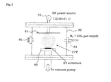
- the carbon nanochips layer can be preferably formed by a plasma CVD method using a gaseous mixture of methane and hydrogen as a raw material. While the specification of the plasma CVD system is not particularly limited, a system using a parallel plate electrode needs to have a configuration in which a plate electrode including a first electrode 81 and a second electrode 82 is arranged in a vacuum chamber 80, of which air is exhausted by a vacuum pump, and a current collector substrate 83 is placed on the second electrode 82 in parallel to the plate electrode, as shown in FIG. 3 . Further, a gaseous mixture of hydrogen and methane is flown between the plate electrodes from a gas inlet port 84 in parallel to the plate electrodes.
- An electric power is input into the first electrode 81 from a RF power source 85, the gaseous mixture is irradiated with an RF wave to become plasma, and a capacitively-coupled plasma atmosphere (CCP) is formed among the first electrode 81, the second electrode 82, and the current collector substrate 83.
- the temperature of the current collector substrate 83 is controlled by a heater (not shown in the drawings) in the second electrode 82.
- the vacuum chamber 80 may be provided with an observation window at a side thereof.
- the plasma CVD system is not limited to the one described above and may have another configuration in which a gaseous mixture is supplied from above the vacuum chamber, as described in PTLs 1 and 3.
- an oxygen cleaning step is performed in which the respective surfaces of the current collector substrate and the electrode for plasma CVD are cleaned with oxygen by generating plasma in the chamber under the presence of oxygen.
- a passive coating film containing iron in the substrate surface can be activated and the carbon nanochips layer can be effectively formed.
- the oxygen cleaning step is preferably performed in the conditions that the flow gas is oxygen, the gas flow rate is 60 sccm, the temperature of the current collector substrate is in the range of 60°C to 200°C, the process pressures is 100 Pa, the time period is 1 hour, the applied high-frequency output is in the range of 100 W to 200 W, and the applied high frequency is 13.56 MHz.
- an amorphous phase is be easily generated when the substrate temperature is set to be not lower than 650°C in the growth conditions described later, and the carbon nanochips layer can be easily formed in which a large number of flake-shaped graphene sheets are grown in different directions, instead of in a vertical direction with respect to the substrate as is the case with known carbon nanowalls, while gaps are being formed among the graphene sheets.
- the plasma CVD method herein is a method for performing chemical vapor-phase growth by generating plasma out of the raw material gas in order to activate a chemical reaction.
- the method conceptually includes high frequency plasma CVD using high frequencies, ECR plasma CVD applying a microwave and an ECR magnetic field, inductively-coupled plasma (ICP) CVD, UHF plasma CVD, VHF plasma CVD, etc, regardless of how the CVD methods perform excitation for plasma generation.
- ICP inductively-coupled plasma
- the following is preferable conditions for the plasma CVD method.
- a flowing gas a gaseous mixture of hydrogen and methane is used.
- the mixture ratio H 2/ CH 4 of hydrogen and methane is preferably in the range of 1/5 to 2/1 so that the carbon nanochips are grown independently from the substrate surface to incline in random directions. The smaller the ratio is, the larger the size of crystallites is and the smaller the g/d ratio is. Since the flow rate of the gaseous mixture depends on the system, an appropriate amount of the mixture needs to be selected according to the system. A flow rate of approximately 10 sccm to 500 sccm is generally desirable.
- the substrate temperature is desirably in the range of 650°C to 850°C.
- the carbon nanochips are desirably grown for roughly 15 minutes to 2 hours under the conditions that the process pressure in the chamber is in the range of 0.05 Torr to 0.5 Torr (6.7 Pa to 66.7 Pa), the applied high-frequency output is in the range of approximately 50 W to 200 W, the applied high frequency is 13.56 MHz, and the distance from the electrode to the current collector substrate is in the range of approximately 20 mm to 30 mm.
- the substrate temperature needs to be not lower than 650°C, preferably higher than 700°C and not higher than 850°C, and more preferably not higher than 800°C.
- a required growth time is 15 minutes or more.
- the height (growth) of the carbon nanochips layer can be controlled by the heating temperature of the substrate and the time of heating the substrate. Specifically, carbon nanochips can be grown to a height of approximately 200 nm in approximately 1 to 2 hours. Since the higher the process pressure in the chamber is, the more difficult it is to form the shape of nanochips, a process pressure of approximately 0.05 Torr to 0.1 Torr (6.7 Pa to 13.3 Pa) is more preferable.
- a bias voltage at the current collector substrate' side is desirably not larger than 0 V in terms of formation of the shape of the nanochips.
- the carbon nanochips layer is easily formed when the bias voltage is not larger than 0 V, and is more easily formed when the bias voltage is in the range of -100 V to 0 V.
- the shape, for example, of the carbon nanochips layer can be controlled by controlling the distance from the substrate to the electrode in implementing the method.
- the distance from the electrode to the current collector substrate is most preferably in the range of 20 mm to 30 mm.
- the distance is not larger than 20 mm, the carbon nanochip is difficult to form and is in the form of a flat plate.
- the distance is larger than 30 mm, the nanochip is in the form of micro particles or a flat plate.
- the silicon thin film layer is preferably formed of gap silicon parts located in the gaps among the carbon nanochips and a silicon thin film layered part in the form of a layer over the carbon nanochips layer.
- the inventors of the present invention have found out that the carbon nanochips layer having the above structure reduces the change in the volume of the silicon as a negative active material caused by charging and discharging, so that separation or cracking is prevented from occurring.
- the silicon thin film desirably includes amorphous silicon, microcrystalline silicon, or a combination of amorphous silicon and crystalline silicon.
- a vapor phase method is desirably used as a method for depositing the silicon thin film layer. While the method specifically includes a CVD method, a sputtering method, a vacuum deposition method, and a thermal spraying method, a vacuum deposition method is the most preferable. This is because when a vacuum deposition method is used for forming the silicon thin film layer, the kinetic energy of deposited silicon particles is smaller than that in the case of using a sputtering method, and gaps therefore generate more easily in the formed silicon thin film layer. Further, silicon parts in the gaps (the gap silicon parts) serve to reduce the change in the volume of the silicon as a negative active material caused by charging and discharging, so that separation or cracking can be prevented from occurring in the silicon thin film layer.
- a thin film is formed on a substrate in such a manner that a heat-resistant container containing a silicon raw material and the substrate are arranged in a vacuum chamber to face each other, the vacuum degree of the chamber is set in the range of 10 -3 Pa to 10 -5 Pa, and the silicon raw material is irradiated with an electron beam emitted from an electron beam source in order that silicon is evaporated.
- the electron beam is accelerated at 4 kV to 8kV.
- the raw material of silicon is heated, evaporated, and deposited on the substrate surface, so that a silicon thin film is formed on the carbon nanochips.
- the film thickness can be adjusted by the time for the deposition.
- the silicon thin film which has a concave-convex surface reflecting a concave-convex surface of the underlying carbon nanochips layer, is favorable when a solid electrolyte layer is formed on the silicon thin film, in that the contacting area of the silicon thin film and the solid electrolyte layer at the boundary therebetween can be increased.
- the silicon thin film can be smoothed by polishing the surface thereof.
- any material is applicable as long as the material is electrically conductive.
- a current collector substrate made of any one of an austenitic stainless steel, a martensitic stainless steel, and a ferritic stainless steel is excellent in the corrosion resistance and achieves a low manufacturing cost.
- the carbon nanochips are grown without requiring a catalyst in the substrate surface, using a substrate made of an iron alloy or a stainless steel is favorable since the iron acts as a catalyst.
- the substrate temperature may exceed 900°C in forming carbon nanochips by a plasma CVD method in a case where the negative current collector substrate is made of a stainless steel
- the substrate temperature is preferably not higher than 850°C since grain growth of graphite is caused by change of mode of graphite crystal growth when the temperature exceeds 900°C.
- a carbon steel, copper, a copper alloy, silicon, a silicon alloy, nickel, a nickel alloy, titanium, or a titanium alloy, which has been generally used for current collector substrates maybe used.
- the practical thickness of the current collector is usually in the range of 100 nm to 300 nm.
- a disc with a side of 0 ⁇ 16 mm is punched in a 1 mm-thick stainless steel (austenitic stainless steel SUS304) sheet and the sheet is used as a negative current collector substrate.
- a 1 mm-thick stainless steel (austenitic stainless steel SUS304) sheet is punched in a 1 mm-thick stainless steel (austenitic stainless steel SUS304) sheet and the sheet is used as a negative current collector substrate.
- the stainless steel sheet in which the disc has been punched is placed in a chamber of a plasma CVD system (see FIG. 3 ) and plasma CVD is performed in the following conditions.
- plasma CVD is performed as well under the condition that the temperature of the current collector substrate is 600°C.
- FIGs. 4 and 5 A chart of a Raman spectrum of the thus obtained sample and a scanning electron microscope photograph of a surface of the sample are shown in FIGs. 4 and 5 , respectively.
- the d' -band which is specific to carbon nanowalls, is clearly observed in the carbon nanochips in the chart of the Raman spectrum.
- the d' -band is not observed and the carbon nanochips are not grown.
- transmissive electron microscope photographs see FIGs. 6 and 7
- electron beam diffraction photograph see FIG. 8
- graphene sheets are flake-shaped sheets grown in irregular directions, the carbon nanochips form significantly small crystals, and charging and discharging as the negative active material is rapidly performed.
- the electron microscope photograph in FIG. 5 shows that although flat carbon crystals characteristic of carbon nanowalls are observed, the crystals are grown to incline in irregular directions independently from the current collector substrate, instead of being grown in a completely vertical direction to the current collector substrate as is the case with the crystals of generally known carbon nanowalls, and that the grown crystals are in contact with each other or close to each other near the destination of the growth.
- silicon is vapor-deposited. In this way, a silicon thin film is formed.
- This vapor deposition is performed by irradiating a silicon target with an electron beam under an argon atmosphere, using an electron beam vapor deposition system. A lithium ion battery negative electrode is thus fabricated.
- FIG. 9 illustrates the stainless steel substrate in the gray part, and the carbon nanochips layer and the silicon thin film layer in the white part on the stainless steel substrate (Part A in FIG. 9).
- FIG. 10 illustrates a bright field image of the frame part A in FIG. 9 magnified three-hundred thousand times.
- FIG. 11 illustrates a bright field image of the boundary part between the carbon nanochips layer and the silicon thin film layer in the frame part B in FIG. 10 , the boundary part being magnified 1.2 million times.
- the silicon thin film layer includes a sequence of silicon thin films formed like a layer on the carbon nanochips layer and that gaps among the carbon nanochips and the upper surface of the carbon nanochips layer are covered with the silicon thin film layered part.
- the carbon nanochips layer and the silicon thin film layered part have thicknesses of approximately 50 nm and 200 nm, respectively.
- the negative electrode fabricated as above and a counter electrode of lithium metal are used to form a 0 ⁇ 20 coin cell secondary battery (half cell; 0 ⁇ 20 coin cell), and the charge/discharge characteristics of the secondary battery are measured.
- An electrolyte solution includes ethylene carbonate and dimethyl carbonate in a volume ratio of 1 : 2, and an electrolyte includes lithium hexafluorophosphate in a concentration of 1 mol/L.
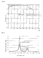
- FIG. 12 illustrates a graph of charge/discharge characteristics.
- the charging/discharging capacities at the first cycle are 232 ⁇ Ah and 147 ⁇ Ah, respectively, and the charging/discharging capacities at the second cycle are 137 ⁇ Ah and 136 ⁇ Ah, respectively.
- the negative electrode fabricated as above is used to form a lithium secondary battery (full cell; 0 ⁇ 20 coin cell).
- a separator 25 is sandwiched between battery containers 21 and 22, a positive electrode 28 containing a positive active material (Li 1-x CoO 2 where x is 0 to 1) having a layered structure and a negative electrode 24 are arranged at both sides of the separator 25, respectively, an aluminum-based current collector 27 is brought into contact with the positive electrode 28 and is further brought into contact with the battery container 22 via a plate spring 26.
- a current collector 23 is brought into contact with the negative electrode 24 and the battery container 21.
- the battery containers 21 and 22 are engaged with each other by an insulating gasket 29.
- an electrolyte solution for lithium ion batteries is added, which is obtained by preparing a mixture solution containing ethylene carbonate and dimethyl carbonate in a volume ratio of 1 : 2 and dissolving LiPF 6 in a concentration of 1 mol/L into the mixture solution.
- FIG. 13 illustrates the charge/discharge characteristics of the thus fabricated lithium secondary battery.
- charging and discharging are repeated at a charging/discharging rate of 50 ⁇ A.
- the capacities at the first, the second, and the third charging/discharging cycles are measured, and the measured values are defines as evaluations of the charge/discharge cycle characteristics.
- the charging/discharging capacities at the first cycle are 999 ⁇ Ah and 494 ⁇ Ah, respectively
- the charging/discharging capacities at the second cycle are 999 ⁇ Ah and 828 ⁇ Ah, respectively
- the charging/discharging capacities at the third cycle are 999 ⁇ Ah and 839 ⁇ Ah, respectively.
- the full cell of Embodiment 1 is a lithium secondary battery having large charging/discharging capacities and a battery capacity which is only slightly reduced due to repeated charging and discharging.
- an oxygen cleaning step is performed in which the respective surfaces of the current collector substrate and the plasma CVD electrode are cleaned with oxygen under the following conditions, prior to the step of forming the carbon nanochips layer by a plasma CVD method in Embodiment 1.
- the other steps in Embodiment 2 are similar to the steps in Embodiment 1 in which the carbon nanochips layer is formed by a plasma CVD method under the condition that the temperature of the substrate is 750°C, and the descriptions thereof will be omitted.
- a generally known carbon nanowall is prepared in Comparative Example 1 under the same conditions as those in Embodiment 1, and is coated with a silicon thin film layer under the same conditions as those in Embodiment 1.
- the carbon nanowall is formed by introducing a CF 4 gas between parallel plate electrodes in a chamber of a CVD system and performing PECVD (plasma-enhanced chemical-vapor deposition) while heating the substrate to a temperature of approximately 500°C.
- the pressure in the chamber is 13.3 Pa and the time of growth is 8 hours.
- the other steps are similar to the steps in Embodiment 2 and the descriptions thereof will be omitted.
- FIG. 14 indicates that the g/d ratio is 0.42 and 0.28 in Embodiment 2 and Comparative Example 1, respectively, which means that the crystallinity level of graphite is lower in Embodiment 2 than in Comparative Example 1.
- the negative electrode prepared as above is used to fabricate a half cell in the same manner as that in Embodiment 1 and the charge/discharge characteristics are measured in the same manner as that in Embodiment 1.
- FIGs. 15 and 16 illustrate the charge/discharge characteristics of the half cell in Embodiment 2 and in Comparative Example 1, respectively.
- the graphs and the weight determined from an X-ray film thickness meter indicate that the charging/discharging capacities are much larger and the charging capacity is more excellent in Embodiment 2 than in Comparative Example 1. Further, it is found that charging and discharging can be repeatedly performed since no significant difference exists in the charge/discharge characteristics between in the first cycle and in the second cycle.
- FIG. 17 illustrates a graph of a derivation curve representing the charge/discharge characteristics in the second cycle in Embodiment 2. This graph suggests generation of SiC. Specifically, broad peaks at 1.2 V and 1.8 V in a positive direction and a broad peak at 0.9 V in a negative direction are peaks associated with oxidation and reduction of SiC.
- the negative electrode prepared as above is used to fabricate a lithium secondary battery (full cell) in the same manner as that in Embodiment 1 and the charge/discharge characteristics are measured.
- FIG. 19 illustrates the charge/discharge characteristics of the thus fabricated lithium secondary battery.
- the charging capacities in the first to sixth cycles are 1000 ⁇ Ah, and the discharging capacities in the first to sixth cycles are 586 ⁇ Ah, 833 ⁇ Ah, 975 ⁇ Ah, 965 ⁇ Ah, 969 ⁇ Ah, and 965 ⁇ Ah, respectively.
- the full cell of Embodiment 2 is a lithium secondary battery having large charging/discharging capacities and a battery capacity which is only slightly reduced due to repeated charging and discharging.
- the negative electrode of the present invention is expected to realize, at a low price, a high performance lithium secondary battery using silicon as a negative active material.
Landscapes
- Chemical & Material Sciences (AREA)
- Engineering & Computer Science (AREA)
- General Chemical & Material Sciences (AREA)
- Chemical Kinetics & Catalysis (AREA)
- Electrochemistry (AREA)
- Materials Engineering (AREA)
- Organic Chemistry (AREA)
- Metallurgy (AREA)
- Mechanical Engineering (AREA)
- Physics & Mathematics (AREA)
- Plasma & Fusion (AREA)
- Manufacturing & Machinery (AREA)
- Inorganic Chemistry (AREA)
- Composite Materials (AREA)
- Battery Electrode And Active Subsutance (AREA)
- Cell Electrode Carriers And Collectors (AREA)
Applications Claiming Priority (2)
| Application Number | Priority Date | Filing Date | Title |
|---|---|---|---|
| JP2012134317 | 2012-06-13 | ||
| PCT/JP2013/066275 WO2013187452A1 (fr) | 2012-06-13 | 2013-06-12 | Électrode négative pour batteries auxiliaires au lithium et son procédé de production |
Publications (2)
| Publication Number | Publication Date |
|---|---|
| EP2736105A1 true EP2736105A1 (fr) | 2014-05-28 |
| EP2736105A4 EP2736105A4 (fr) | 2015-04-29 |
Family
ID=49758270
Family Applications (1)
| Application Number | Title | Priority Date | Filing Date |
|---|---|---|---|
| EP13805172.7A Withdrawn EP2736105A4 (fr) | 2012-06-13 | 2013-06-12 | Électrode négative pour batteries auxiliaires au lithium et son procédé de production |
Country Status (6)
| Country | Link |
|---|---|
| US (1) | US9368795B2 (fr) |
| EP (1) | EP2736105A4 (fr) |
| JP (1) | JP5906261B2 (fr) |
| KR (1) | KR20150027022A (fr) |
| CN (1) | CN103718347A (fr) |
| WO (1) | WO2013187452A1 (fr) |
Cited By (3)
| Publication number | Priority date | Publication date | Assignee | Title |
|---|---|---|---|---|
| EP2913870A4 (fr) * | 2012-10-29 | 2016-06-08 | Sango Co Ltd | Électrode négative pour élément de batterie secondaire au lithium-ion et son procédé de fabrication |
| CN115298857A (zh) * | 2020-04-01 | 2022-11-04 | 富士通商株式会社 | 蓄电设备及蓄电设备用电极 |
| IT202100017024A1 (it) * | 2021-06-29 | 2022-12-29 | Pierfrancesco Atanasio | Elettrodi ibridi carbonio/materiale attivo per accumulatori agli ioni di litio |
Families Citing this family (40)
| Publication number | Priority date | Publication date | Assignee | Title |
|---|---|---|---|---|
| US20110294005A1 (en) * | 2010-05-28 | 2011-12-01 | Semiconductor Energy Laboratory Co., Ltd. | Power storage device, electrode, and electric device |
| JP6055729B2 (ja) * | 2013-07-10 | 2016-12-27 | 株式会社豊田自動織機 | リチウムイオン二次電池用負極及びリチウムイオン二次電池 |
| JP6367652B2 (ja) * | 2014-08-27 | 2018-08-01 | 国立研究開発法人物質・材料研究機構 | シリコン(Si)系ナノ構造材料及びその製造方法 |
| US9219402B2 (en) * | 2015-06-11 | 2015-12-22 | Dennis D McCrady | EcoCharge power plant |
| KR101879502B1 (ko) * | 2015-09-11 | 2018-07-18 | 한양대학교 산학협력단 | 계면층이 도입된 이차전지용 음극 및 이의 제조방법 |
| CN108138302B (zh) * | 2015-10-02 | 2020-12-22 | 应用材料公司 | 用于制造柔性层堆叠的方法和设备、用于制造锂电池的负极的方法以及用于锂电池的负极 |
| KR102553839B1 (ko) | 2015-12-24 | 2023-07-10 | 삼성전자주식회사 | 리튬이차전지 |
| US11171324B2 (en) | 2016-03-15 | 2021-11-09 | Honda Motor Co., Ltd. | System and method of producing a composite product |
| US11383213B2 (en) | 2016-03-15 | 2022-07-12 | Honda Motor Co., Ltd. | System and method of producing a composite product |
| JP6563364B2 (ja) * | 2016-05-31 | 2019-08-21 | 株式会社三五 | 二次電池用負極 |
| CN105977447B (zh) * | 2016-07-21 | 2018-08-21 | 苏州协鑫集成科技工业应用研究院有限公司 | 负极片及其制备方法及电池 |
| KR102244058B1 (ko) | 2016-08-24 | 2021-04-22 | 삼성에스디아이 주식회사 | 리튬 이차 전지용 음극 활물질 및 이를 포함하는 리튬 이차 전지 |
| CN106601989B (zh) * | 2016-12-19 | 2019-06-28 | 华中科技大学 | 一种多孔薄膜电极材料及其制备方法 |
| US11081684B2 (en) | 2017-05-24 | 2021-08-03 | Honda Motor Co., Ltd. | Production of carbon nanotube modified battery electrode powders via single step dispersion |
| US10658651B2 (en) | 2017-07-31 | 2020-05-19 | Honda Motor Co., Ltd. | Self standing electrodes and methods for making thereof |
| US20190036102A1 (en) | 2017-07-31 | 2019-01-31 | Honda Motor Co., Ltd. | Continuous production of binder and collector-less self-standing electrodes for li-ion batteries by using carbon nanotubes as an additive |
| US11201318B2 (en) | 2017-09-15 | 2021-12-14 | Honda Motor Co., Ltd. | Method for battery tab attachment to a self-standing electrode |
| US11121358B2 (en) | 2017-09-15 | 2021-09-14 | Honda Motor Co., Ltd. | Method for embedding a battery tab attachment in a self-standing electrode without current collector or binder |
| CN107619042A (zh) * | 2017-10-09 | 2018-01-23 | 南昌大学 | 一种大规模制备石墨烯纳米墙的方法 |
| CN109778137B (zh) * | 2017-11-14 | 2020-09-25 | 中国科学院过程工程研究所 | 一种碳钢复合材料及其制备方法和用途 |
| CN109873113B (zh) * | 2017-12-04 | 2020-12-04 | 钰邦科技股份有限公司 | 锂电池结构及其锂电池负电极箔 |
| US11673807B2 (en) | 2018-06-11 | 2023-06-13 | National University Corporation Tokai National Higher Education And Research System | Carbon nanostructured materials and methods for forming carbon nanostructured materials |
| CN109616630B (zh) * | 2018-11-27 | 2021-12-21 | 哈尔滨工业大学(深圳) | 一种均匀碳膜和垂直石墨烯双重包覆的硅-碳复合材料及其制备方法与锂离子电池应用 |
| US11535517B2 (en) | 2019-01-24 | 2022-12-27 | Honda Motor Co., Ltd. | Method of making self-standing electrodes supported by carbon nanostructured filaments |
| CN111490253B (zh) * | 2019-01-29 | 2021-12-10 | 宁德时代新能源科技股份有限公司 | 一种负极极片及其锂离子二次电池 |
| US12381275B2 (en) | 2019-01-30 | 2025-08-05 | Honda Motor Co., Ltd. | Stretchable and flexible lithium ion battery |
| US12142771B2 (en) | 2019-01-30 | 2024-11-12 | Honda Motor Co., Ltd. | Flexible battery as an integration platform for wearable sensors and processing/transmitting devices |
| US11325833B2 (en) | 2019-03-04 | 2022-05-10 | Honda Motor Co., Ltd. | Composite yarn and method of making a carbon nanotube composite yarn |
| US11352258B2 (en) | 2019-03-04 | 2022-06-07 | Honda Motor Co., Ltd. | Multifunctional conductive wire and method of making |
| US11539042B2 (en) | 2019-07-19 | 2022-12-27 | Honda Motor Co., Ltd. | Flexible packaging with embedded electrode and method of making |
| EP3859033B1 (fr) * | 2019-11-14 | 2023-09-13 | Proterial, Ltd. | Feuille pour collecteur de courant d'électrode négative d'une cellule secondaire |
| CN111584828A (zh) * | 2020-04-28 | 2020-08-25 | 江西昌大高新能源材料技术有限公司 | 一种锂离子电池硅/金属复合薄膜负极结构及其制备方法 |
| CA3151456A1 (fr) * | 2020-07-14 | 2022-01-20 | Joshua J. LAU | Materiau d'electrode comprenant de l'oxyde de silicium et des nanotubes de carbone monoparois |
| CN111969186B (zh) * | 2020-07-22 | 2021-09-28 | 自贡兴川储能技术有限公司 | 一种以石墨烯为骨架的硅碳薄膜负极及制备方法 |
| KR102320909B1 (ko) | 2021-05-07 | 2021-11-02 | 한밭대학교 산학협력단 | 탄소 나노월 및 이의 제조방법, 이를 포함하는 리튬 이차전지용 음극 |
| KR102872098B1 (ko) * | 2021-08-12 | 2025-10-15 | 주식회사 엘지에너지솔루션 | 리튬 이차전지용 음극 및 이의 제조방법 |
| CN115966658A (zh) * | 2021-10-11 | 2023-04-14 | 南方科技大学 | 硅复合纳米纤维、硅复合纳米纤维膜及其制备方法和应用 |
| CN114784253B (zh) * | 2022-05-20 | 2024-05-10 | 电子科技大学 | 用于二次电池的氧化亚硅碳复合负极材料及制备和应用 |
| CN119731119B (zh) * | 2022-09-20 | 2026-02-03 | 尤米科尔公司 | 在蓄电池的负电极中使用的复合粉末以及包括此类复合粉末的蓄电池 |
| JP7675352B2 (ja) * | 2022-12-30 | 2025-05-13 | 国立大学法人東海国立大学機構 | 蓄電デバイス用電極、二次電池、および、蓄電デバイス用電極の製造方法 |
Family Cites Families (35)
| Publication number | Priority date | Publication date | Assignee | Title |
|---|---|---|---|---|
| GB2168966B (en) | 1984-11-14 | 1988-09-01 | Toho Beslon Co | High-strength carbonaceous fiber |
| JP4997674B2 (ja) | 2001-09-03 | 2012-08-08 | 日本電気株式会社 | 二次電池用負極および二次電池 |
| JP2003077529A (ja) | 2001-09-03 | 2003-03-14 | Sanyo Electric Co Ltd | リチウム電池及びリチウム二次電池 |
| US20030129305A1 (en) | 2002-01-08 | 2003-07-10 | Yihong Wu | Two-dimensional nano-sized structures and apparatus and methods for their preparation |
| EP1576678A2 (fr) | 2002-09-10 | 2005-09-21 | California Institute Of Technology | Silicium nanostructure grande capacite et alliages de lithium correspondants |
| EP1661855A4 (fr) | 2003-08-27 | 2012-01-18 | Mineo Hiramatsu | Procede de production de nanoparoi en carbone, nanoparoi en carbone, et appareil de production correspondant |
| JP4853861B2 (ja) * | 2005-04-05 | 2012-01-11 | 国立大学法人京都工芸繊維大学 | カーボンナノ構造体の形成方法及び装置 |
| WO2007000940A1 (fr) | 2005-06-28 | 2007-01-04 | Konica Minolta Medical & Graphic, Inc. | Procédé et dispositif de détection d’ombre anormale candidate |
| JP5162825B2 (ja) * | 2005-12-13 | 2013-03-13 | パナソニック株式会社 | 非水電解質二次電池用負極とそれを用いた非水電解質二次電池 |
| FR2895572B1 (fr) | 2005-12-23 | 2008-02-15 | Commissariat Energie Atomique | Materiau a base de nanotubes de carbone et de silicium utilisable dans des electrodes negatives pour accumulateur au lithium |
| KR100763892B1 (ko) | 2006-01-20 | 2007-10-05 | 삼성에스디아이 주식회사 | 음극 활물질, 그 제조 방법, 및 이를 채용한 음극과 리튬전지 |
| JP5309317B2 (ja) | 2006-09-08 | 2013-10-09 | 古河電気工業株式会社 | カーボンナノ構造体の製造方法及び製造装置 |
| JP2008239357A (ja) | 2007-03-25 | 2008-10-09 | Univ Nagoya | カーボンナノウォールの製造方法 |
| US8828481B2 (en) | 2007-04-23 | 2014-09-09 | Applied Sciences, Inc. | Method of depositing silicon on carbon materials and forming an anode for use in lithium ion batteries |
| JP2009164104A (ja) * | 2007-09-06 | 2009-07-23 | Canon Inc | 負極用電極材料、その製造方法ならびに該材料を用いた電極構造体及び蓄電デバイス |
| CN101808819A (zh) | 2007-09-07 | 2010-08-18 | 无机专家公司 | 作为用于锂二次电池的阳极材料的硅改性纳米纤维纸 |
| US8119288B2 (en) | 2007-11-05 | 2012-02-21 | Nanotek Instruments, Inc. | Hybrid anode compositions for lithium ion batteries |
| US7745047B2 (en) * | 2007-11-05 | 2010-06-29 | Nanotek Instruments, Inc. | Nano graphene platelet-base composite anode compositions for lithium ion batteries |
| US9564629B2 (en) | 2008-01-02 | 2017-02-07 | Nanotek Instruments, Inc. | Hybrid nano-filament anode compositions for lithium ion batteries |
| US8435676B2 (en) | 2008-01-09 | 2013-05-07 | Nanotek Instruments, Inc. | Mixed nano-filament electrode materials for lithium ion batteries |
| US20090186276A1 (en) * | 2008-01-18 | 2009-07-23 | Aruna Zhamu | Hybrid nano-filament cathode compositions for lithium metal or lithium ion batteries |
| US8968820B2 (en) | 2008-04-25 | 2015-03-03 | Nanotek Instruments, Inc. | Process for producing hybrid nano-filament electrodes for lithium batteries |
| US8936874B2 (en) | 2008-06-04 | 2015-01-20 | Nanotek Instruments, Inc. | Conductive nanocomposite-based electrodes for lithium batteries |
| JP5412638B2 (ja) | 2008-06-27 | 2014-02-12 | 公立大学法人横浜市立大学 | リチウムイオン電池用負極材料及びそれを用いた急速充放電型リチウムイオン電池 |
| US20110104551A1 (en) * | 2009-11-05 | 2011-05-05 | Uchicago Argonne, Llc | Nanotube composite anode materials suitable for lithium ion battery applications |
| JP5130275B2 (ja) | 2009-11-11 | 2013-01-30 | トヨタ自動車株式会社 | リチウム二次電池用負極およびその製造方法 |
| WO2011137448A2 (fr) * | 2010-04-30 | 2011-11-03 | University Of Southern California | Électrodes nanostructurées silicium-carbone |
| US20110281156A1 (en) * | 2010-05-17 | 2011-11-17 | Arthur Douglas Boren | Vertically Aligned Carbon Nanotube Augmented lithium Ion Anode for Batteries |
| JP5851756B2 (ja) * | 2010-08-10 | 2016-02-03 | 株式会社デンソー | 炭素ナノ構造体、金属担持炭素ナノ構造体、リチウムイオン2次電池、炭素ナノ構造体の製造方法、及び金属担持炭素ナノ構造体の製造方法 |
| DE102010039416A1 (de) * | 2010-08-17 | 2012-02-23 | Varta Micro Innovation Gmbh | Flexible Batterieelektroden und ihre Herstellung |
| KR101201804B1 (ko) * | 2011-04-21 | 2012-11-15 | 삼성에스디아이 주식회사 | 리튬 이차 전지용 음극, 이의 제조 방법 및 이를 포함하는 리튬 이차 전지 |
| WO2013027561A1 (fr) * | 2011-08-19 | 2013-02-28 | Semiconductor Energy Laboratory Co., Ltd. | Procédé permettant de fabriquer un objet revêtu de graphène, électrode négative de batterie rechargeable incluant l'objet revêtu de graphène et batterie rechargeable incluant l'électrode négative |
| JP6034621B2 (ja) * | 2011-09-02 | 2016-11-30 | 株式会社半導体エネルギー研究所 | 蓄電装置の電極および蓄電装置 |
| JP6016597B2 (ja) * | 2011-12-16 | 2016-10-26 | 株式会社半導体エネルギー研究所 | リチウムイオン二次電池用正極の製造方法 |
| US10553871B2 (en) * | 2012-05-04 | 2020-02-04 | Zenlabs Energy, Inc. | Battery cell engineering and design to reach high energy |
-
2013
- 2013-06-12 WO PCT/JP2013/066275 patent/WO2013187452A1/fr not_active Ceased
- 2013-06-12 EP EP13805172.7A patent/EP2736105A4/fr not_active Withdrawn
- 2013-06-12 US US14/240,190 patent/US9368795B2/en not_active Expired - Fee Related
- 2013-06-12 CN CN201380002456.5A patent/CN103718347A/zh active Pending
- 2013-06-12 JP JP2013556082A patent/JP5906261B2/ja active Active
- 2013-06-12 KR KR1020147001490A patent/KR20150027022A/ko not_active Abandoned
Cited By (6)
| Publication number | Priority date | Publication date | Assignee | Title |
|---|---|---|---|---|
| EP2913870A4 (fr) * | 2012-10-29 | 2016-06-08 | Sango Co Ltd | Électrode négative pour élément de batterie secondaire au lithium-ion et son procédé de fabrication |
| US9520595B2 (en) | 2012-10-29 | 2016-12-13 | Sango Co., Ltd. | Negative electrode for lithium-ion secondary cell and method for manufacturing same |
| CN115298857A (zh) * | 2020-04-01 | 2022-11-04 | 富士通商株式会社 | 蓄电设备及蓄电设备用电极 |
| EP4131459A4 (fr) * | 2020-04-01 | 2024-05-08 | Fujitusyou Co., Ltd. | Dispositif de stockage d'énergie et électrode pour dispositif de stockage d'énergie |
| IT202100017024A1 (it) * | 2021-06-29 | 2022-12-29 | Pierfrancesco Atanasio | Elettrodi ibridi carbonio/materiale attivo per accumulatori agli ioni di litio |
| WO2023275733A1 (fr) * | 2021-06-29 | 2023-01-05 | Nanoshare 4.0 Srl | Électrodes hybrides carbone/matériau actif pour batteries au lithium-ion |
Also Published As
| Publication number | Publication date |
|---|---|
| JPWO2013187452A1 (ja) | 2016-02-08 |
| WO2013187452A1 (fr) | 2013-12-19 |
| EP2736105A4 (fr) | 2015-04-29 |
| JP5906261B2 (ja) | 2016-04-20 |
| US9368795B2 (en) | 2016-06-14 |
| KR20150027022A (ko) | 2015-03-11 |
| US20140170490A1 (en) | 2014-06-19 |
| CN103718347A (zh) | 2014-04-09 |
Similar Documents
| Publication | Publication Date | Title |
|---|---|---|
| US9368795B2 (en) | Lithium secondary battery negative electrode and method for manufacturing the same | |
| JP7654633B2 (ja) | バッテリーアノードとして使用するためのケイ素組成物材料 | |
| CN102282705B (zh) | 用于在柔性衬底上制造碳纳米结构的工艺、以及包括柔性碳纳米结构电极的能量存储器件 | |
| US10403889B2 (en) | High-capacity silicon nanowire based anode for lithium-ion batteries | |
| JP5095863B2 (ja) | リチウムイオン電池用負極およびその製造方法、ならびにリチウムイオン電池 | |
| JP4351732B2 (ja) | リチウム二次電池用電極およびそれを備えたリチウム二次電池 | |
| Forney et al. | High performance silicon free-standing anodes fabricated by low-pressure and plasma-enhanced chemical vapor deposition onto carbon nanotube electrodes | |
| US20100151318A1 (en) | Three-dimensional battery with hybrid nano-carbon layer | |
| JP2021116191A (ja) | 複合炭素材料及びリチウムイオン二次電池 | |
| JP5036161B2 (ja) | リチウムイオン二次電池用負極活物質、その製造方法、およびそれを用いたリチウムイオン二次電池 | |
| CN104798226B (zh) | 锂离子二次电池用负极及其制造方法 | |
| US20170054138A1 (en) | Ultra-high output power and extremely robust cycle life negative electrode material for lithium secondary battery and method for manufacturing the same, using layer structure of metal oxide nanoparticles and porous graphene | |
| Kim et al. | Straightforward fabrication of a highly branched graphene nanosheet array for a Li-ion battery anode | |
| JP2009078956A (ja) | カーボンナノチューブ複合体、これを用いたエネルギーデバイス及びカーボンナノチューブ複合体の製造方法 | |
| Kim et al. | Novel hybrid Si film/carbon nanofibers as anode materials in lithium-ion batteries | |
| Govindarajan et al. | Sputter-deposited binder-free nanopyramidal Cr/γ-Mo2N TFEs for high-performance supercapacitors | |
| TWI521774B (zh) | Lithium secondary battery negative electrode and manufacturing method thereof | |
| JP7576785B2 (ja) | カーボンナノウォール電極及びその製造方法 | |
| Kim et al. | Novel hybrid Si film/highly branched graphene nanosheets for anode materials in lithium-ion batteries | |
| WO2022221427A1 (fr) | Nanorubans de graphène en tant que matériaux d'électrode dans des dispositifs de stockage d'énergie | |
| CN116324013A (zh) | 形成阴极层的方法,形成电池组半电池的方法 | |
| WO2014014376A1 (fr) | Batterie ion lithium à base de matériau nano-structurel tridimensionnel multicouches | |
| Lin et al. | The Effects of Power Levels/Time Periods for Sputtering Cobalt onto Carbon Nanotubes/Graphene Composites and Cobalt Annealed on the Characteristics of Anode Materials for Lithium‐Ion Batteries | |
| JP2023182286A (ja) | シリコンナノワイヤーの製造方法、シリコンナノワイヤー群、電池用電極 |
Legal Events
| Date | Code | Title | Description |
|---|---|---|---|
| PUAI | Public reference made under article 153(3) epc to a published international application that has entered the european phase |
Free format text: ORIGINAL CODE: 0009012 |
|
| 17P | Request for examination filed |
Effective date: 20140224 |
|
| AK | Designated contracting states |
Kind code of ref document: A1 Designated state(s): AL AT BE BG CH CY CZ DE DK EE ES FI FR GB GR HR HU IE IS IT LI LT LU LV MC MK MT NL NO PL PT RO RS SE SI SK SM TR |
|
| RA4 | Supplementary search report drawn up and despatched (corrected) |
Effective date: 20150331 |
|
| RIC1 | Information provided on ipc code assigned before grant |
Ipc: H01M 4/587 20100101ALI20150325BHEP Ipc: C23C 16/26 20060101ALI20150325BHEP Ipc: H01M 4/62 20060101ALI20150325BHEP Ipc: H01M 4/134 20100101AFI20150325BHEP Ipc: H01M 4/38 20060101ALI20150325BHEP Ipc: C23C 16/509 20060101ALI20150325BHEP Ipc: H01M 4/1395 20100101ALI20150325BHEP Ipc: H01M 4/36 20060101ALI20150325BHEP Ipc: H01M 4/66 20060101ALI20150325BHEP |
|
| DAX | Request for extension of the european patent (deleted) | ||
| 17Q | First examination report despatched |
Effective date: 20151118 |
|
| GRAP | Despatch of communication of intention to grant a patent |
Free format text: ORIGINAL CODE: EPIDOSNIGR1 |
|
| INTG | Intention to grant announced |
Effective date: 20161223 |
|
| STAA | Information on the status of an ep patent application or granted ep patent |
Free format text: STATUS: THE APPLICATION IS DEEMED TO BE WITHDRAWN |
|
| 18D | Application deemed to be withdrawn |
Effective date: 20170503 |