EP2736181A1 - Dispositif, procédé et programme de transmission optique - Google Patents
Dispositif, procédé et programme de transmission optique Download PDFInfo
- Publication number
- EP2736181A1 EP2736181A1 EP13192286.6A EP13192286A EP2736181A1 EP 2736181 A1 EP2736181 A1 EP 2736181A1 EP 13192286 A EP13192286 A EP 13192286A EP 2736181 A1 EP2736181 A1 EP 2736181A1
- Authority
- EP
- European Patent Office
- Prior art keywords
- signal
- unit
- drive signal
- modulation unit
- linear characteristic
- Prior art date
- Legal status (The legal status is an assumption and is not a legal conclusion. Google has not performed a legal analysis and makes no representation as to the accuracy of the status listed.)
- Granted
Links
Images


Classifications
-
- H—ELECTRICITY
- H04—ELECTRIC COMMUNICATION TECHNIQUE
- H04B—TRANSMISSION
- H04B10/00—Transmission systems employing electromagnetic waves other than radio-waves, e.g. infrared, visible or ultraviolet light, or employing corpuscular radiation, e.g. quantum communication
- H04B10/50—Transmitters
- H04B10/516—Details of coding or modulation
-
- H—ELECTRICITY
- H04—ELECTRIC COMMUNICATION TECHNIQUE
- H04B—TRANSMISSION
- H04B10/00—Transmission systems employing electromagnetic waves other than radio-waves, e.g. infrared, visible or ultraviolet light, or employing corpuscular radiation, e.g. quantum communication
- H04B10/50—Transmitters
- H04B10/501—Structural aspects
- H04B10/503—Laser transmitters
- H04B10/505—Laser transmitters using external modulation
- H04B10/5053—Laser transmitters using external modulation using a parallel, i.e. shunt, combination of modulators
-
- H—ELECTRICITY
- H04—ELECTRIC COMMUNICATION TECHNIQUE
- H04B—TRANSMISSION
- H04B10/00—Transmission systems employing electromagnetic waves other than radio-waves, e.g. infrared, visible or ultraviolet light, or employing corpuscular radiation, e.g. quantum communication
- H04B10/50—Transmitters
- H04B10/58—Compensation for non-linear transmitter output
- H04B10/588—Compensation for non-linear transmitter output in external modulation systems
-
- H—ELECTRICITY
- H04—ELECTRIC COMMUNICATION TECHNIQUE
- H04J—MULTIPLEX COMMUNICATION
- H04J14/00—Optical multiplex systems
- H04J14/06—Polarisation multiplex systems
-
- H—ELECTRICITY
- H04—ELECTRIC COMMUNICATION TECHNIQUE
- H04L—TRANSMISSION OF DIGITAL INFORMATION, e.g. TELEGRAPHIC COMMUNICATION
- H04L27/00—Modulated-carrier systems
- H04L27/18—Phase-modulated carrier systems, i.e. using phase-shift keying
- H04L27/20—Modulator circuits; Transmitter circuits
- H04L27/2096—Arrangements for directly or externally modulating an optical carrier
Definitions
- a certain aspect of embodiments described herein relates to an optical transmission device, a method of optical transmission, and a program of optical transmission.
- Japanese Patent Application Publication No. 2010-109705 discloses a technology in which a digital signal process on a side of transmission is performed with respect to a signal input into a modulator in order to achieve a long-distance and large-capacity communication system. In an optical transmission device, it is preferable that a non-linear characteristic of the modulator is compensated for.
- the present invention has been made in view of those circumstances, and an object thereof is to provide an optical transmission device, a method of optical transmission, and a program of optical transmission that are capable of compensating for a non-linear characteristic of a modulator.
- an optical transmission device including: a drive signal generate unit that generates a drive signal; a modulation unit that modulates an optical signal in accordance with the drive signal; a detect unit that detects a fluctuation of a signal component of the drive signal with respect to an optical signal output by the modulation unit; and a correct unit that corrects a parameter of the drive signal generate unit in accordance with a detect result of the detect unit so that a non-linear characteristic of the modulation unit gets closer to a linear characteristic.
- non-linear characteristic of a modulator it is difficult to compensate for a non-linear characteristic of a modulator because the non-linear characteristic may fluctuate according to a wave form such as amplitude or a frequency of a drive signal.
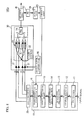
- FIG. 1 illustrates a block diagram of a main structure of an optical transmission device 100 in accordance with a first embodiment.
- the optical transmission device 100 has a digital signal processing unit 10, a D/A converter 20, a polarization-multiplexing modulation unit 30, a branch unit 41, a light-receiving unit 42, a filter 43, a detect unit 44, a correct unit 45 and so on.
- the digital signal processing unit 10 has a FEC encode unit 11, a symbol mapping unit 12, a semi-fixed pre-equalize unit 13, a carrier frequency control unit 14, a signal spectrum shape unit 15 and a transmission FE (Front End) compensate unit 16.
- the digital signal processing unit 10 acts as a drive signal generate unit for generating a drive signal.
- the polarization-multiplexing modulation unit 30 has a plurality of electrical amplifiers 31, a light source 32, a QPSK modulation units 33a and 33b, and a multiplex unit 34.
- the QPSK modulation units 33a and 33b are used.
- a modulator that is capable of multiple-value modulating such as a 16QAM may be used.
- the FEC encode unit 11 performs an encoding of FEC (Forward Error Correction) with respect to a main signal (input signal) that is input into the digital signal processing unit 10.
- the symbol mapping unit 12 performs a symbol mapping of phase with respect to a signal received from the FEC encode unit 11.
- the semi-fixed pre-equalize unit 13 performs a pre-equalizing process with respect to a signal received from the symbol mapping unit 12.
- the carrier frequency control unit 14 controls a frequency of a carrier wave of a signal received from the semi-fixed pre-equalize unit 13.
- the signal spectrum shape unit 15 performs a shaping process with respect to a spectrum of a signal received from the carrier frequency control unit 14.
- the transmission FE compensate unit 16 performs a compensating process of a linear characteristic or the like with respect to a signal received from the signal spectrum shape unit 15.
- the digital signal processing unit 10 outputs a drive signal as a result of the processes of each unit.
- the D/A convertor 20 is a digital/analog convertor that converts each drive signal (a digital signal) output by the digital signal processing unit 10 into an analog signal.
- the D/A convertor 20 converts each drive signal output from the digital signal processing unit 10 into a drive signal IX of an I-component of an X-polarization wave, a drive signal QX of a Q-component of the X-polarization wave, a drive signal IY of an I-component of a Y-polarization wave, and a drive signal QY of a Q-component of the Y-polarization wave.
- the I-component is an In-phase component.
- the Q-component is a Quadrature component.
- the polarization-multiplexing modulation unit 30 outputs a modulation signal by modulating the I-component and the Q-component of each polarization wave of an output light of the light source 32 and multiplexing the modulated components.
- the electrical amplifier 31 is not limited to a specific amplifier.
- the electrical amplifier 31 is, for example, a semiconductor amplifier.
- the electrical amplifier 31 is provided according to each component of the X-polarization wave and the Y-polarization wave. In the embodiment, the number of the electrical amplifier 31 is four in accordance with each component of the X-polarization wave and the Y-polarization wave.
- Each electrical amplifier 31 amplifies each component of the X-polarization wave and the Y-polarization wave output by the D/A convertor 20 to an adequate drive amplitude and applies the amplified components to the QPSK modulation units 33a and 33b.
- the light source 32 is not limited to a specific light source.
- the light source 32 is, for example, a semiconductor laser.
- the QPSK modulation units 33a and 33b respectively have two Mach-Zehnder modulation units in parallel. Modulation units in the QPSK modulation units 33a and 33b are not limited to a specific modulation unit.
- the modulated units are, for example, a Mach-Zehnder modulation unit using an electrooptical crystal such as a LiNbO 3 (LN) substrate or a LiTaO 2 substrate.
- the QPSK modulation unit 33a acts as a modulator for the X-polarization wave
- the QPSK modulation unit 33b acts as a modulator for the Y-polarization wave.
- a light output by the light source 32 is divided into four components of the I-component and the Q-component of the X-polarization wave and the Y-polarization wave, and input into a waveguide of each modulation unit of the QPSK modulation units 33a and 33b.
- Each drive signal output by each electrical amplifier 31 is applied to an arm of each modulation unit.
- the QPSK modulation unit 33a outputs a QPSK modulation signal of the X-polarization wave.
- the QPSK modulation unit 33b outputs a QPSK modulation signal of the Y-polarization wave.
- the multiplex unit 34 is a PBC (Polarization Beam Combiner) for multiplexing the QPSK modulation signals output by the QPSK modulation units 33a and 33b.
- the modulation signal multiplexed by the multiplex unit 34 is output as an optical signal.
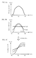
- FIG. 2A illustrates an input-output characteristic of a typical electrical amplifier.
- the electrical amplifier has a non-linear characteristic in which output amplitude is saturated gradually as input amplitude increases.
- the electrical amplifier 31 of the embodiment has the characteristic of FIG. 2A.
- FIG. 2B illustrates an extinction characteristic of a normal Mach-Zehnder. With reference to FIG. 2B , an output optical intensity of the Mach-Zehnder modulation unit approximately has a cyclic characteristic of a square of cosine with respect to a bias voltage applied to the Mach-Zehnder modulation unit.
- each modulation unit of the QPSK modulation units 33a and 33b has the extinction characteristic of FIG. 2B .
- the polarization-multiplexing modulation unit 30 has a non-linear characteristic as a whole because of the non-linear characteristics of the electrical amplifier and the modulation unit.
- the polarization-multiplexing modulation unit 30 has the non-linear characteristic. Therefore, a modulation signal obtained by applying of a drive signal differs from a modulation signal that is estimated in a case where the polarization-multiplexing modulation unit 30 has a linear characteristic. And so, the optical transmission device 100 superimposes a signal component reflected in the modulation signal output by the polarization-multiplexing modulation unit 30 to a drive signal as a superimposed signal, and detects the non-linear characteristic of the polarization-multiplexing modulation unit 30 by detecting a changing of the reflection of the superimposed signal.
- the transmission FE compensate unit 16 of the digital signal processing unit 10 compensates for the detected non-linear characteristic.
- a description will be given of an example of a compensation of non-linear characteristic in which the electrical amplifier 31 and the Mach-Zehnder modulation unit for the I-component of the QPSK modulation unit 33a.
- a drive signal F(t) a superimposed signal h(t) is superimposed in a reference signal f(t).
- the drive signal F(t) f(t) + h(t) is input into the electrical amplifier 31 for the I-component of the QPSK modulation unit 33a.
- FIG. 3A illustrates the reference signal f(t).
- the reference signal f(t) indicates amplitude after amplification of the electrical amplifier 31.
- the reference signal f(t) is a signal of which frequency fluctuates in accordance with a time.
- the frequency of the reference signal f(t) fluctuates from f1 to f3, and gets higher as the time passes.
- the amplitude of the reference signal f(t) corresponds to a voltage of 2V ⁇ corresponding to a mountain (a local maximum value), a valley (a local minimum value) and another mountain (another local maximum ) of the extinction characteristic of each Mach-Zehnder modulation unit.
- FIG. 3B illustrates the superimposed signal h(t).
- the superimposed signal h(t) is a signal of which frequency is constant.
- the amplitude of the superimposed signal h(t) is smaller than that of the reference signal f(t), and may be adjusted in accordance with a sensitivity in a signal detection.
- the D/A convertor 20 has a port for outputting the drive signal F(t) and another port for outputting the reference signal f(t) in addition to the port.
- the D/A convertor 20 outputs the reference signal f(t) from the another port and inputs the reference signal f(t) into the detect unit 44. That is, the D/A convertor 20 acts as an input unit for inputting the reference signal to the detect unit 44.
- the branch unit 41 branches a part of an optical signal output by a Mach-Zehnder modulation unit that is an objective of detection and inputs the branched signal into the light-receiving unit 42.
- the light-receiving unit 42 converts the optical signal into an electrical signal by a photoelectric conversion.
- the filter 43 extracts a signal component corresponding to the superimposed signal h(t) from an electrical signal output by the light-receiving unit 42.
- the detect unit 44 is an oscilloscope or the like, and monitors the above-mentioned signal component with use of the reference signal f(t) output from the second port of the D/A convertor 20.
- the waveform is a wave form in a section in which the frequency of the reference signal f(t) is f1 in the drive signal F(t) of FIG. 3C .
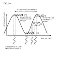
- Voltages V1, V2, and Vc of FIG. 5A are respectively a bottom voltage V1, a top voltage V2 and a center voltage between V1 and V2 in a fluctuation of photofield illustrated in an upper part of FIG. 4 .
- Voltages V1, V2 and Vc of FIG. 5A are respectively a left local maximum peak voltage V1, a right local maximum peak voltage V2 and a center voltage Vc (a local minimum peak) between V1 and V2 in an extinction curve illustrated in a lower part of FIG. 3 .
- the superimposed signal h(t) changes because of the non-linear characteristic of the electrical amplifier 31 and the Mach-Zehnder modulation unit.
- the non-linear characteristic of the Mach-Zehnder modulation unit appears strongly around the voltage V1 and the voltage V2. Because of the non-linear characteristic, a distortion may occur in the superimposed signal h(t). Thus, an intensity of the signal component extracted by the filter 43 gets smaller.
- the characteristic of the Mach-Zehnder modulation unit is approximately linear near the voltage Vc. Therefore, the intensity of the signal component extracted by the filter 43 becomes a maximum.
- the non-linear characteristic of the Mach-Zehnder modulation unit is a frequency response characteristic. Therefore, the non-linear characteristic changes in accordance with a frequency when amplitude of an input drive signal is constant.
- the non-linear characteristic of the electrical amplifier 31 may fluctuate in accordance with a frequency of an input drive signal.
- FIG. 5B illustrates an overlapped graph of non-linear characteristic of each frequency.
- FIG. 5B illustrates a waveform in a case where f(t 1 ) at time t 1 is Acos ⁇ 1 t 1 , f(t 2 ) at time t 2 is Acos ⁇ 2 t 2 , and f(t 3 ) at time t 3 is Acos ⁇ 3 t 3 .
- a relation f(t 1 ) ⁇ f(t 2 ) ⁇ f(t 3 ) is satisfied.
- the non-linear characteristic of the electrical amplifier 31 and the Mach-Zehnder modulation unit fluctuates in accordance with a frequency of an input drive signal. In concrete, when the frequency gets higher, the non-linear characteristic of the electrical amplifier 31 and the Mach-Zehnder modulation unit is reduced and a characteristic close to a linear characteristic appears.
- FIG. 5B approximately linear characteristic is obtained when f(t 3 ) is Acos ⁇ 3 t 3 . Therefore, an intensity of a signal component extracted by the filter 43 is detected as an approximately constant value in spite of a drive voltage.
- the detect unit 44 detects a non-linear characteristic at each frequency of the electrical amplifier 31 and the Mach-Zehnder modulation unit by integrating the characteristic obtained in FIG. 5B.
- FIG. 5C illustrates a non-linear characteristic of the electrical amplifier 31 and the Mach-Zehnder modulation unit obtained by integrating. When the electrical amplifier 31 has a linear characteristic, FIG. 5C is a non-linear characteristic of the Mach-Zehnder modulation unit.
- the correct unit 45 corrects a parameter of the transmission FE compensate unit 16 so that the non-linear characteristic detected by the detect unit 44 gets closer to a linear characteristic (the non-linear characteristic is reduced). It is preferable that the correct unit 45 generates an opposite characteristic to achieve a linear characteristic by being multiplied by the non-linear characteristic detected by the detect unit 44 as illustrated in FIG. 6B to FIG. 6D , and a parameter achieving the opposite characteristic is set in the transmission FE compensate unit 16.
- FIG. 7 illustrates an example of a flowchart executed by the optical transmission device 100.
- the digital signal processing unit 10 selects a port to be measured (Step S1).
- the port to be measured is a combination of one of the Mach-Zehnder modulation units of the QPSK modulation units 33a and 33b and one of the electrical amplifiers 31 applying a signal to the one of the Mach-Zehnder modulation units.
- the digital signal processing unit 10 applies a drive signal F(t) to the Mach-Zehnder-modulation unit of the selected port (Step S2).
- the D/A convertor 20 outputs the reference signal f(t) from the second port (Step S3).
- "n” is a natural number from “1” to “m”.
- the detect unit 44 determines whether "n” reaches "m” (Step S5). When it is determined as “No” in the Step S5, "n+1” is substituted into “n”, and the Step S4 is executed again.
- the detect unit 44 detects a non-linear characteristic at each frequency of the electrical amplifier 31 and the Mach-Zehnder modulation unit of the selected port by integrating a waveform at each time t n (Step S6).
- the correct unit 45 calculates a characteristic opposite to the non-linear characteristic detected by the detect unit 44 (Step S7).
- the correct unit 45 sets a parameter of the transmission FE compensate unit 16 so that a calculated opposite characteristic is achieved (Step S8). After that, the execution of the flow chart is terminated.
- the flow chart of FIG. 7 is executed with respect to each port, the whole non-linear characteristic of the polarization-multiplexing modulation unit 30 is compensated for.
- a reflection result of a superimposed signal fluctuating according to the non-linear characteristic of the polarization-multiplexing modulation unit 30 It is therefore possible to detect the non-linear characteristic of the polarization-multiplexing modulation unit 30. And, the parameter of the transmission FE compensate unit 16 is corrected so that the non-linear characteristic is reduced (close to a linear characteristic). Therefore, the non-linear characteristic of the polarization-multiplexing modulation unit 30 can be compensated for. It is therefore possible to improve an effect of a function such as a non-linear pre-equalization of a transmission line performed in the digital signal processing unit 10.
- a polarization-multiplexing modulator is used as the polarization-multiplexing modulation unit 30.
- the structure is not limited.
- a modulator having a Mach-Zehnder modulator in which a non-linear characteristic appears in an extinction characteristic can be applied to the non-linear characteristic compensation of the embodiment.
- the amplitude of the reference signal f(t) applied to each modulation unit is set to be 2V ⁇ . However, the amplitude may be different from 2V ⁇ .
- FIG. 8 illustrates a block diagram of a main structure of an optical transmission device 100a in accordance with a second embodiment.
- the optical transmission device 100a is different from the optical transmission device 100 of FIG. 1 in points that the filter 43 is not provided, the D/A convertor 20 does not have the second port, and a signal superimpose unit 46 is provided.
- signal amplitude of a drive signal input into each Mach-Zehnder modulation unit is changed in a given period. An average of the signal amplitude is changed. Thereby, the non-linear characteristic of the polarization-multiplexing modulation unit 30 is detected.
- the signal superimpose unit 46 inputs a low-frequency signal f0 having a frequency f0 into each electrical amplifier 31.
- the low-frequency signal f0 is superimposed to a drive signal output by each electrical amplifier 31 as a superimposed signal.
- the signal amplitude of the drive signal output by each electrical amplifier 31 changes in a period of the frequency f0.
- the non-linear characteristic of the polarization-multiplexing modulation unit 30 is detected based on a changing of the low-frequency signal f0 in a case where the average amplitude of the drive signal output by the electrical amplifier 31 is changed with the low-frequency signal f0 being superimposed.
- FIG. 9A illustrates an extinction characteristic of each Mach-Zehnder modulation unit.
- a bias voltage is set so that a center voltage of the drive signal output by the electrical amplifier 31 approximately corresponds to a valley (a local minimum value) of the extinction characteristic. This setting is achieved when a normal bias control is performed.
- the signal superimpose unit 46 superimposes the low-frequency signal f0 at a point where the center voltage of the drive signal corresponds to the valley (a local minimum value) of the extinction characteristic.
- the digital signal processing unit 10 changes the average amplitude of the drive signal output by the electrical amplifier 31 with the low-frequency signal f0 being superimposed.
- the digital signal processing unit 10 acts as an amplitude control unit that changes the average amplitude of the drive signal.
- the changing of the reflection of the low-frequency signal f0 with respect to the optical signal output by the polarization-multiplexing modulation unit 30 is detected. It is possible to detect the non-linear characteristic of the polarization-multiplexing modulation unit 30, by detecting the changing of the reflection.
- FIG. 10 illustrates an intensity changing of the low-frequency signal f0 according to a changing of amplitude of the drive signal output by the electrical amplifier 31.
- an absolute value of an inclination is a maximum value around a center between the mountain (a local maximum value) and the valley (a local minimum value).
- a detected intensity of the low-frequency signal f0 becomes maximum.
- the absolute value of the inclination gets smaller as the position gets away from the center between the mountain (a local maximum) and the valley (a local minimum). Therefore, the intensity of the detected frequency signal f0 gets smaller.
- a fluctuation range of the low-frequency signal f0 exceeds the mountain (a local maximum) or valley (a local minimum). Therefore, a component of frequency 2f0 can be detected. However, the low-frequency signal f0 is not detected. Therefore, when the amplitude of the drive signal output by the electrical amplifier 31 is 2V ⁇ , the optical signal output by the polarization-multiplexing modulation unit 30 does not include the low-frequency signal f0. Further, when the drive amplitude output by the electrical amplifier 31 is increased, the low-frequency signal f0 to be superimposed is compressed because of the non-linear characteristic (saturation characteristic) of the electrical amplifier 31. And a detected component gets smaller.
- FIG. 11B illustrates an intensity changing of the low-frequency signal f0 caused by the non-linear characteristic of the electrical amplifier 31.
- FIG. 11C illustrates an intensity changing of the low-frequency signal f0 caused by the non-linear characteristic of each modulation unit of the polarization-multiplexing modulation unit 30.
- FIG. 11A illustrates a non-linear characteristic, the sum of FIG. 11B and FIG. 11C .
- FIG. 12 illustrates an example of a flowchart executed by the optical transmission device 100a.
- the digital signal processing unit 10 selects a port to be measured (Step S11).
- the port to be measured is a combination of one of Mach-Zehnder modulation units of the QPSK modulation units 33a and 33b and one of the electrical amplifiers 31 that applies a signal to the Mach-Zehnder modulation unit.
- the digital signal processing unit 10 sets a center of a bias so that the center of the bias corresponds to a valley (local minimum) of an extinction characteristic by executing a bias control of the selected port (Step S12).
- the bias control is temporarily stopped.
- the signal superimpose unit 46 superimposes the low-frequency signal f0 to the electrical amplifier 31 of the selected port (Step S13).
- the digital signal processing unit 10 changes the average amplitude of the signal output by the electrical amplifier 31 by changing the amplitude of the drive signal input into the electrical amplifier 31 (Step S14).
- the detect unit 44 detects a non-linear characteristic of the selected port by detecting a signal component according to the low-frequency signal f0 from an optical signal output by the polarization-multiplexing modulation unit 30 (Step S15).
- the correct unit 45 calculates an opposite characteristic of the non-linear characteristic detected in the Step S15 (Step S16).
- the correct unit 45 sets a parameter of the transmission FE compensate unit 16 so that the calculated opposite characteristic is achieved (Step S17). After that, the execution of the flow chart is terminated.
- the flowchart of FIG. 12 is performed with respect to each port, the non-linear characteristic of the polarization multiplexing modulation unit 30 is compensate for.
- a result of a superimposed signal changing according to the non-linear characteristic of the polarization-multiplexing modulation unit 30 is detected. It is therefore possible to detect the non-linear characteristic of the polarization-multiplexing modulation unit 30.
- the parameter of the transmission FE compensate unit 16 is corrected so that the non-linear characteristic is reduced (close to a linear characteristic). Therefore, the non-characteristic of the polarization-multiplexing modulation unit 30 can be compensated for. It is therefore possible to improve the function effect such as a non-linear pre-equalization of a transmission line performed in the digital signal processing unit 10.
- the polarization-multiplexing modulation unit 30 is used as a modulation unit.
- the structure is not limited.
- the non-linear characteristic compensation can be applied to a modulation unit having a Mach-Zehnder modulation unit in which a non-linear characteristic appears in an extinction characteristic.
- the amplitude of the drive signal output by the electrical amplifier 31 is changed by changing the amplitude of the drive signal input into the electrical amplifier 31.
- the structure is not limited.
- the amplitude of the drive signal output by the electrical amplifier 31 may be changed by changing a gain of the electrical amplifier 31. That is, the electrical amplifier 31 acts as a frequency control unit for changing the average amplitude of the drive signal.
- FIG. 13 illustrates a block diagram of a main structure of an optical transmission device 100b in accordance with a third embodiment.
- the optical transmission device 100b is different from the optical transmission device 100 of FIG. 1 in a point that a VOA (Variable Optical Attenuator) 47 is provided.
- the variable optical attenuator 47 is provided after the branch unit 41 and adjusts an optical intensity of a modulation signal output by the polarization-multiplexing modulation unit 30.
- the variable optical attenuator 47 may acts as a shut unit that shuts off the outputting of the optical signal from the polarization-multiplexing modulation unit 30.
- the non-linear characteristic of the polarization-multiplexing modulation unit 30 may be detected after the outputting of the modulation signal from the polarization-multiplexing modulation unit 30 is shut off, and the parameter of the transmission FE compensate unit 16 may be set. In this case, it is suppressed that an outer component is broken down because of the modulation signal output during detecting the non-linear characteristic.
- the variable optical attenuator 47 may be provided after the branch unit 41.
- FIG. 14 illustrates a block diagram of a hardware structure of the digital signal processing unit 10, the detect unit 44 and the correct unit 45.
- the digital signal processing unit 10, the detect unit 44 and the correct unit 45 have a CPU 101, a RAM 102, a storage device 103, an interface 104 and so on. These components are connected via a bus or the like.
- the CPU 101 is a Central Processing Unit.
- the CPU 101 includes one or more core.
- the RAM (Random Access Memory) 102 is a volatile memory for temporarily storing a program executed by the CPU 101, a data processed by the CPU 101 and so on.
- the storage device 103 is non-volatile storage device.
- a ROM (Read Only Memory), a solid state drive (SSD) such as a flash memory, a hard disk driven by a hard disk drive or the like can be used as the storage device 103.
- the digital signal processing unit 10, the detect unit 44 and the correct unit 45 are realized in the optical transmission devices 100, 100a and 100b.
- the digital signal processing unit 10, the detect unit 44 and the correct unit 45 may be a hardware such as a dedicated circuit or the like.
Landscapes
- Physics & Mathematics (AREA)
- Engineering & Computer Science (AREA)
- Computer Networks & Wireless Communication (AREA)
- Signal Processing (AREA)
- Electromagnetism (AREA)
- Nonlinear Science (AREA)
- Optics & Photonics (AREA)
- Optical Communication System (AREA)
- Optical Modulation, Optical Deflection, Nonlinear Optics, Optical Demodulation, Optical Logic Elements (AREA)
Applications Claiming Priority (1)
| Application Number | Priority Date | Filing Date | Title |
|---|---|---|---|
| JP2012255440A JP6031963B2 (ja) | 2012-11-21 | 2012-11-21 | 光送信装置、光送信方法、および光送信プログラム |
Publications (2)
| Publication Number | Publication Date |
|---|---|
| EP2736181A1 true EP2736181A1 (fr) | 2014-05-28 |
| EP2736181B1 EP2736181B1 (fr) | 2019-03-13 |
Family
ID=49554123
Family Applications (1)
| Application Number | Title | Priority Date | Filing Date |
|---|---|---|---|
| EP13192286.6A Not-in-force EP2736181B1 (fr) | 2012-11-21 | 2013-11-11 | Dispositif, procédé et programme de transmission optique |
Country Status (3)
| Country | Link |
|---|---|
| US (1) | US9564975B2 (fr) |
| EP (1) | EP2736181B1 (fr) |
| JP (1) | JP6031963B2 (fr) |
Families Citing this family (14)
| Publication number | Priority date | Publication date | Assignee | Title |
|---|---|---|---|---|
| JP2565702Y2 (ja) | 1991-11-26 | 1998-03-18 | 東海旅客鉄道株式会社 | レール締結金具緊解装置 |
| JP2522880Y2 (ja) | 1992-06-30 | 1997-01-16 | 石川島播磨重工業株式会社 | レール締結金具自動着脱装置 |
| JP6036210B2 (ja) * | 2012-11-19 | 2016-11-30 | 富士通株式会社 | エンファシス信号生成回路 |
| JP6108939B2 (ja) * | 2013-04-25 | 2017-04-05 | 三菱電機株式会社 | 光送受信機 |
| JP6519999B2 (ja) * | 2014-07-16 | 2019-05-29 | 富士通株式会社 | 光送信装置及び検出装置 |
| JP6435764B2 (ja) * | 2014-10-09 | 2018-12-12 | 富士通株式会社 | 光送信器、光変調器の制御方法、及び、光変調器の制御装置 |
| JP6502663B2 (ja) * | 2014-12-24 | 2019-04-17 | 日本オクラロ株式会社 | 光通信装置 |
| JP6522964B2 (ja) * | 2015-01-28 | 2019-05-29 | 日本オクラロ株式会社 | 光送受信器 |
| JP6350762B2 (ja) | 2015-03-20 | 2018-07-04 | 日本電気株式会社 | 光送信器および光通信方法 |
| CN106878207B (zh) * | 2015-12-11 | 2021-07-13 | 富士通株式会社 | 测量滤波特性的方法及其装置、预均衡器、通信设备 |
| JP6589659B2 (ja) * | 2016-01-21 | 2019-10-16 | 富士通株式会社 | 伝送装置及び伝送方法 |
| JP6733395B2 (ja) * | 2016-07-25 | 2020-07-29 | 富士通株式会社 | 光送信器、光受信器、および光伝送方法 |
| US10887022B2 (en) * | 2017-06-15 | 2021-01-05 | Nokia Of America Corporation | Backward propagation with compensation of some nonlinear effects of polarization mode dispersion |
| JP7011534B2 (ja) * | 2018-05-29 | 2022-02-10 | 日本電信電話株式会社 | 制御回路 |
Citations (6)
| Publication number | Priority date | Publication date | Assignee | Title |
|---|---|---|---|---|
| US5161044A (en) * | 1989-07-11 | 1992-11-03 | Harmonic Lightwaves, Inc. | Optical transmitters linearized by means of parametric feedback |
| US6671465B1 (en) * | 2000-04-07 | 2003-12-30 | Lucent Technologies Inc. | Apparatus and methods for improving linearity and noise performance of an optical source |
| US20080130083A1 (en) * | 2006-12-01 | 2008-06-05 | Fujitsu Limited | Drive apparatus for an optical modulator with a ternary drive signal, optical transmitter, and optical transmission system |
| US7426350B1 (en) * | 2001-10-26 | 2008-09-16 | Cisco Technology, Inc. | Hybrid optical and electrical fiber optic link linearizer |
| US20100104284A1 (en) * | 2008-10-23 | 2010-04-29 | Xiang Liu | System, method and apparatus for joint self phase modulation compensation for coherent optical polarization-division-multiplexed orthogonal-frequency division-multiplexing systems |
| JP2010109705A (ja) | 2008-10-30 | 2010-05-13 | Fujitsu Ltd | 光送受信システム,光送信器,光受信器および光送受信方法 |
Family Cites Families (45)
| Publication number | Priority date | Publication date | Assignee | Title |
|---|---|---|---|---|
| EP0407919B1 (fr) * | 1989-07-11 | 1996-04-24 | Harmonic Lightwaves, Inc. | Emetteurs optiques linéarisés au moyen de contre-réaction paramétrique |
| US5850305A (en) * | 1996-12-18 | 1998-12-15 | Scientific-Atlanta, Inc. | Adaptive predistortion control for optical external modulation |
| US6374000B1 (en) * | 1996-12-23 | 2002-04-16 | Dsc Communications A/S | Method and an apparatus for modulating light in a modulator circuit comprising Mach-Zehnder modulator |
| JP3913856B2 (ja) * | 1997-08-28 | 2007-05-09 | 富士通株式会社 | 光パルス生成装置、分散測定装置、分散補償装置及び分散測定方法 |
| JP3723358B2 (ja) * | 1998-11-25 | 2005-12-07 | 富士通株式会社 | 光変調装置及び光変調器の制御方法 |
| JP2000241778A (ja) * | 1999-02-19 | 2000-09-08 | Fujitsu Ltd | 光通信装置および光分岐・挿入装置 |
| JP2004508737A (ja) * | 1999-09-02 | 2004-03-18 | オルテル コーポレーション | 複合2次バイアス制御方式 |
| US6687466B1 (en) * | 2000-01-06 | 2004-02-03 | Adc Telecommunications, Inc. | Dynamic distortion control |
| JP2002023122A (ja) * | 2000-06-30 | 2002-01-23 | Mitsubishi Electric Corp | 光送信装置およびこれに用いる光変調器のバイアス電圧制御方法 |
| KR100381014B1 (ko) * | 2000-11-01 | 2003-04-26 | 한국전자통신연구원 | 선형 광 변조기를 이용하여 진폭 잡음을 억제시킨 광 세기변조 장치 및 그 방법 |
| JP4646048B2 (ja) * | 2001-03-02 | 2011-03-09 | 日本電気株式会社 | 単一側波帯信号光の生成方法および単一側波帯信号光の生成回路 |
| JP3772738B2 (ja) * | 2001-12-13 | 2006-05-10 | 日本電気株式会社 | 光変調装置 |
| JP3881270B2 (ja) * | 2002-03-26 | 2007-02-14 | 富士通株式会社 | 光変調器の駆動制御装置および駆動制御方法 |
| US7308210B2 (en) * | 2002-04-05 | 2007-12-11 | Kabushiki Kaisha Toshiba | Optical modulating device, optical transmitting apparatus using the same, method of controlling optical modulating device, and control program recording medium |
| JP2004061956A (ja) * | 2002-07-30 | 2004-02-26 | Fujitsu Ltd | 光送信装置及びその制御方法 |
| US7382984B2 (en) * | 2002-10-03 | 2008-06-03 | Nortel Networks Limited | Electrical domain compensation of optical dispersion in an optical communications system |
| JP2004247968A (ja) * | 2003-02-13 | 2004-09-02 | Fujitsu Ltd | 光送信器 |
| JP4149298B2 (ja) * | 2003-03-27 | 2008-09-10 | 富士通株式会社 | 光変調器の制御装置 |
| US7340184B2 (en) * | 2003-05-01 | 2008-03-04 | Optium Corporation | Linearized Optical Transmitter Using Feedback Control |
| US7412174B2 (en) * | 2004-05-05 | 2008-08-12 | Emcore Corporation | Method and apparatus for distortion control for optical transmitters |
| US7155071B2 (en) * | 2005-03-08 | 2006-12-26 | Harris Corporation | Device for Mach-Zehnder modulator bias control for duobinary optical transmission and associated system and method |
| JP4922594B2 (ja) * | 2005-05-23 | 2012-04-25 | 富士通株式会社 | 光送信装置、光受信装置、およびそれらを含む光通信システム |
| JP4422661B2 (ja) * | 2005-08-31 | 2010-02-24 | 富士通株式会社 | 差動4位相偏移変調器の駆動電圧設定方法 |
| US7539360B2 (en) * | 2005-09-23 | 2009-05-26 | Fujitsu Limited | Monitoring modulator bias using photon absorption |
| US7630651B2 (en) * | 2005-10-21 | 2009-12-08 | Fujitsu Limited | Method and apparatus for controlling bias point of optical transmitter |
| US8532499B2 (en) * | 2005-10-25 | 2013-09-10 | Emcore Corporation | Optical transmitter with adaptively controlled optically linearized modulator |
| JP4781094B2 (ja) * | 2005-11-30 | 2011-09-28 | 富士通株式会社 | 光送信装置 |
| JP4563944B2 (ja) * | 2006-01-31 | 2010-10-20 | 富士通株式会社 | 光送信器 |
| JP4935093B2 (ja) * | 2006-02-02 | 2012-05-23 | 横河電機株式会社 | 光変調装置 |
| JP4910476B2 (ja) * | 2006-05-22 | 2012-04-04 | 富士通株式会社 | 光通信装置 |
| JP2008039929A (ja) * | 2006-08-02 | 2008-02-21 | Nec Corp | 光送信システム及び光送信器,光送信方法、光送信用プログラム |
| JP5405716B2 (ja) * | 2006-09-29 | 2014-02-05 | 富士通株式会社 | 光送信機 |
| JP2008141671A (ja) * | 2006-12-05 | 2008-06-19 | Fujitsu Ltd | 光変調装置、光送信器および光伝送システム |
| US8582981B2 (en) * | 2007-01-15 | 2013-11-12 | Fujitsu Limited | Optical transmitter and control method therefor |
| WO2008111223A1 (fr) * | 2007-03-15 | 2008-09-18 | Fujitsu Limited | Emetteur optique |
| JP5211528B2 (ja) * | 2007-03-29 | 2013-06-12 | 富士通株式会社 | 光変調装置および光変調方式切替方法 |
| JP5476697B2 (ja) * | 2008-09-26 | 2014-04-23 | 富士通株式会社 | 光信号送信装置 |
| US8175465B2 (en) * | 2008-11-12 | 2012-05-08 | Lockheed Martin Corporation | Bias control apparatus and method for optical modulator |
| JP5353387B2 (ja) * | 2009-04-06 | 2013-11-27 | 富士通株式会社 | 光変調器の駆動方法および駆動装置、並びに、それを用いた光送信器 |
| JP2011022479A (ja) * | 2009-07-17 | 2011-02-03 | Mitsubishi Electric Corp | 多値光送信器 |
| JP5195677B2 (ja) * | 2009-07-28 | 2013-05-08 | 富士通株式会社 | 光信号送信装置および偏波多重光信号の制御方法 |
| JP5506575B2 (ja) * | 2010-07-08 | 2014-05-28 | 三菱電機株式会社 | 光変調器、光送信装置およびバイアス調整方法 |
| JP5853386B2 (ja) * | 2010-12-16 | 2016-02-09 | 富士通オプティカルコンポーネンツ株式会社 | 光変調装置および光変調制御方法 |
| US8705983B2 (en) * | 2011-03-25 | 2014-04-22 | Emcore Corporation | Radio frequency optical communication system |
| US8897654B1 (en) * | 2012-06-20 | 2014-11-25 | The United States Of America As Represented By The Administrator Of The National Aeronautics And Space Administration | System and method for generating a frequency modulated linear laser waveform |
-
2012
- 2012-11-21 JP JP2012255440A patent/JP6031963B2/ja not_active Expired - Fee Related
-
2013
- 2013-11-08 US US14/075,369 patent/US9564975B2/en not_active Expired - Fee Related
- 2013-11-11 EP EP13192286.6A patent/EP2736181B1/fr not_active Not-in-force
Patent Citations (6)
| Publication number | Priority date | Publication date | Assignee | Title |
|---|---|---|---|---|
| US5161044A (en) * | 1989-07-11 | 1992-11-03 | Harmonic Lightwaves, Inc. | Optical transmitters linearized by means of parametric feedback |
| US6671465B1 (en) * | 2000-04-07 | 2003-12-30 | Lucent Technologies Inc. | Apparatus and methods for improving linearity and noise performance of an optical source |
| US7426350B1 (en) * | 2001-10-26 | 2008-09-16 | Cisco Technology, Inc. | Hybrid optical and electrical fiber optic link linearizer |
| US20080130083A1 (en) * | 2006-12-01 | 2008-06-05 | Fujitsu Limited | Drive apparatus for an optical modulator with a ternary drive signal, optical transmitter, and optical transmission system |
| US20100104284A1 (en) * | 2008-10-23 | 2010-04-29 | Xiang Liu | System, method and apparatus for joint self phase modulation compensation for coherent optical polarization-division-multiplexed orthogonal-frequency division-multiplexing systems |
| JP2010109705A (ja) | 2008-10-30 | 2010-05-13 | Fujitsu Ltd | 光送受信システム,光送信器,光受信器および光送受信方法 |
Also Published As
| Publication number | Publication date |
|---|---|
| JP2014103594A (ja) | 2014-06-05 |
| US9564975B2 (en) | 2017-02-07 |
| JP6031963B2 (ja) | 2016-11-24 |
| US20140140707A1 (en) | 2014-05-22 |
| EP2736181B1 (fr) | 2019-03-13 |
Similar Documents
| Publication | Publication Date | Title |
|---|---|---|
| EP2736181B1 (fr) | Dispositif, procédé et programme de transmission optique | |
| CN101552636B (zh) | 光调制器及其控制方法和装置 | |
| CN112583492B (zh) | 用于调整光发射器的方法和装置 | |
| US9244328B2 (en) | Optical modulator and optical modulation control method | |
| EP2464038A1 (fr) | Transmetteur optique et procédé de transmission optique | |
| JP5682633B2 (ja) | 光送信器および光信号送信方法 | |
| EP2624484A1 (fr) | Émetteur optique et procédé de commande de polarisation pour modulateur optique | |
| US20150236792A1 (en) | Optical transmitter and dc bias control method | |
| US10341027B2 (en) | Optical transmitter and control method for optical transmitter | |
| US10177852B2 (en) | Method and apparatus for automatically controlling bias voltage of optical modulator | |
| US20180088359A1 (en) | Optical module that includes optical modulator and bias control method for optical modulator | |
| US7561797B1 (en) | Optical signal transmitter with active optical e-field degradation | |
| EP2259128B1 (fr) | Émetteur optique basé sur un processeur de signaux numériques | |
| JP6231434B2 (ja) | 光送信器および線形性調整方法 | |
| WO2017056440A1 (fr) | Modulateur optique, émetteur optique, et procédé de modulation optique | |
| JP6073152B2 (ja) | 光多値信号送信器、光多値信号送受信器及び光多値信号処理ic | |
| CN112005159B (zh) | 光调制器 | |
| CN114095091B (zh) | 布里渊微波光子滤波器带宽扩展方法及系统 | |
| US20140016172A1 (en) | Mach-Zehnder Modulator Drive Level Optimization | |
| US20070003281A1 (en) | Active control loop for power control of optical channel groups | |
| US20200033642A1 (en) | Optical transmitter and optical transmission method | |
| Basak et al. | Photodetector linearization using adaptive electronic post-distortion | |
| CN110581737A (zh) | Iq调制器的控制方法与装置 |
Legal Events
| Date | Code | Title | Description |
|---|---|---|---|
| PUAI | Public reference made under article 153(3) epc to a published international application that has entered the european phase |
Free format text: ORIGINAL CODE: 0009012 |
|
| 17P | Request for examination filed |
Effective date: 20131111 |
|
| AK | Designated contracting states |
Kind code of ref document: A1 Designated state(s): AL AT BE BG CH CY CZ DE DK EE ES FI FR GB GR HR HU IE IS IT LI LT LU LV MC MK MT NL NO PL PT RO RS SE SI SK SM TR |
|
| AX | Request for extension of the european patent |
Extension state: BA ME |
|
| R17P | Request for examination filed (corrected) |
Effective date: 20141106 |
|
| RBV | Designated contracting states (corrected) |
Designated state(s): AL AT BE BG CH CY CZ DE DK EE ES FI FR GB GR HR HU IE IS IT LI LT LU LV MC MK MT NL NO PL PT RO RS SE SI SK SM TR |
|
| STAA | Information on the status of an ep patent application or granted ep patent |
Free format text: STATUS: EXAMINATION IS IN PROGRESS |
|
| 17Q | First examination report despatched |
Effective date: 20180118 |
|
| REG | Reference to a national code |
Ref country code: DE Ref legal event code: R079 Ref document number: 602013052190 Country of ref document: DE Free format text: PREVIOUS MAIN CLASS: H04B0010500000 Ipc: H04J0014060000 |
|
| RIC1 | Information provided on ipc code assigned before grant |
Ipc: H04B 10/516 20130101ALI20180625BHEP Ipc: H04J 14/06 20060101AFI20180625BHEP Ipc: H04L 27/20 20060101ALI20180625BHEP Ipc: H04B 10/50 20130101ALI20180625BHEP Ipc: H04B 10/588 20130101ALI20180625BHEP |
|
| GRAP | Despatch of communication of intention to grant a patent |
Free format text: ORIGINAL CODE: EPIDOSNIGR1 |
|
| STAA | Information on the status of an ep patent application or granted ep patent |
Free format text: STATUS: GRANT OF PATENT IS INTENDED |
|
| INTG | Intention to grant announced |
Effective date: 20181022 |
|
| GRAS | Grant fee paid |
Free format text: ORIGINAL CODE: EPIDOSNIGR3 |
|
| GRAA | (expected) grant |
Free format text: ORIGINAL CODE: 0009210 |
|
| STAA | Information on the status of an ep patent application or granted ep patent |
Free format text: STATUS: THE PATENT HAS BEEN GRANTED |
|
| AK | Designated contracting states |
Kind code of ref document: B1 Designated state(s): AL AT BE BG CH CY CZ DE DK EE ES FI FR GB GR HR HU IE IS IT LI LT LU LV MC MK MT NL NO PL PT RO RS SE SI SK SM TR |
|
| REG | Reference to a national code |
Ref country code: GB Ref legal event code: FG4D |
|
| REG | Reference to a national code |
Ref country code: CH Ref legal event code: EP Ref country code: AT Ref legal event code: REF Ref document number: 1109134 Country of ref document: AT Kind code of ref document: T Effective date: 20190315 |
|
| REG | Reference to a national code |
Ref country code: IE Ref legal event code: FG4D |
|
| REG | Reference to a national code |
Ref country code: DE Ref legal event code: R096 Ref document number: 602013052190 Country of ref document: DE |
|
| REG | Reference to a national code |
Ref country code: NL Ref legal event code: MP Effective date: 20190313 |
|
| REG | Reference to a national code |
Ref country code: LT Ref legal event code: MG4D |
|
| PG25 | Lapsed in a contracting state [announced via postgrant information from national office to epo] |
Ref country code: LT Free format text: LAPSE BECAUSE OF FAILURE TO SUBMIT A TRANSLATION OF THE DESCRIPTION OR TO PAY THE FEE WITHIN THE PRESCRIBED TIME-LIMIT Effective date: 20190313 Ref country code: NO Free format text: LAPSE BECAUSE OF FAILURE TO SUBMIT A TRANSLATION OF THE DESCRIPTION OR TO PAY THE FEE WITHIN THE PRESCRIBED TIME-LIMIT Effective date: 20190613 Ref country code: SE Free format text: LAPSE BECAUSE OF FAILURE TO SUBMIT A TRANSLATION OF THE DESCRIPTION OR TO PAY THE FEE WITHIN THE PRESCRIBED TIME-LIMIT Effective date: 20190313 Ref country code: FI Free format text: LAPSE BECAUSE OF FAILURE TO SUBMIT A TRANSLATION OF THE DESCRIPTION OR TO PAY THE FEE WITHIN THE PRESCRIBED TIME-LIMIT Effective date: 20190313 |
|
| PG25 | Lapsed in a contracting state [announced via postgrant information from national office to epo] |
Ref country code: BG Free format text: LAPSE BECAUSE OF FAILURE TO SUBMIT A TRANSLATION OF THE DESCRIPTION OR TO PAY THE FEE WITHIN THE PRESCRIBED TIME-LIMIT Effective date: 20190613 Ref country code: GR Free format text: LAPSE BECAUSE OF FAILURE TO SUBMIT A TRANSLATION OF THE DESCRIPTION OR TO PAY THE FEE WITHIN THE PRESCRIBED TIME-LIMIT Effective date: 20190614 Ref country code: RS Free format text: LAPSE BECAUSE OF FAILURE TO SUBMIT A TRANSLATION OF THE DESCRIPTION OR TO PAY THE FEE WITHIN THE PRESCRIBED TIME-LIMIT Effective date: 20190313 Ref country code: LV Free format text: LAPSE BECAUSE OF FAILURE TO SUBMIT A TRANSLATION OF THE DESCRIPTION OR TO PAY THE FEE WITHIN THE PRESCRIBED TIME-LIMIT Effective date: 20190313 Ref country code: HR Free format text: LAPSE BECAUSE OF FAILURE TO SUBMIT A TRANSLATION OF THE DESCRIPTION OR TO PAY THE FEE WITHIN THE PRESCRIBED TIME-LIMIT Effective date: 20190313 Ref country code: NL Free format text: LAPSE BECAUSE OF FAILURE TO SUBMIT A TRANSLATION OF THE DESCRIPTION OR TO PAY THE FEE WITHIN THE PRESCRIBED TIME-LIMIT Effective date: 20190313 |
|
| REG | Reference to a national code |
Ref country code: AT Ref legal event code: MK05 Ref document number: 1109134 Country of ref document: AT Kind code of ref document: T Effective date: 20190313 |
|
| PG25 | Lapsed in a contracting state [announced via postgrant information from national office to epo] |
Ref country code: RO Free format text: LAPSE BECAUSE OF FAILURE TO SUBMIT A TRANSLATION OF THE DESCRIPTION OR TO PAY THE FEE WITHIN THE PRESCRIBED TIME-LIMIT Effective date: 20190313 Ref country code: IT Free format text: LAPSE BECAUSE OF FAILURE TO SUBMIT A TRANSLATION OF THE DESCRIPTION OR TO PAY THE FEE WITHIN THE PRESCRIBED TIME-LIMIT Effective date: 20190313 Ref country code: SK Free format text: LAPSE BECAUSE OF FAILURE TO SUBMIT A TRANSLATION OF THE DESCRIPTION OR TO PAY THE FEE WITHIN THE PRESCRIBED TIME-LIMIT Effective date: 20190313 Ref country code: CZ Free format text: LAPSE BECAUSE OF FAILURE TO SUBMIT A TRANSLATION OF THE DESCRIPTION OR TO PAY THE FEE WITHIN THE PRESCRIBED TIME-LIMIT Effective date: 20190313 Ref country code: PT Free format text: LAPSE BECAUSE OF FAILURE TO SUBMIT A TRANSLATION OF THE DESCRIPTION OR TO PAY THE FEE WITHIN THE PRESCRIBED TIME-LIMIT Effective date: 20190713 Ref country code: ES Free format text: LAPSE BECAUSE OF FAILURE TO SUBMIT A TRANSLATION OF THE DESCRIPTION OR TO PAY THE FEE WITHIN THE PRESCRIBED TIME-LIMIT Effective date: 20190313 Ref country code: AL Free format text: LAPSE BECAUSE OF FAILURE TO SUBMIT A TRANSLATION OF THE DESCRIPTION OR TO PAY THE FEE WITHIN THE PRESCRIBED TIME-LIMIT Effective date: 20190313 Ref country code: EE Free format text: LAPSE BECAUSE OF FAILURE TO SUBMIT A TRANSLATION OF THE DESCRIPTION OR TO PAY THE FEE WITHIN THE PRESCRIBED TIME-LIMIT Effective date: 20190313 |
|
| PG25 | Lapsed in a contracting state [announced via postgrant information from national office to epo] |
Ref country code: SM Free format text: LAPSE BECAUSE OF FAILURE TO SUBMIT A TRANSLATION OF THE DESCRIPTION OR TO PAY THE FEE WITHIN THE PRESCRIBED TIME-LIMIT Effective date: 20190313 Ref country code: PL Free format text: LAPSE BECAUSE OF FAILURE TO SUBMIT A TRANSLATION OF THE DESCRIPTION OR TO PAY THE FEE WITHIN THE PRESCRIBED TIME-LIMIT Effective date: 20190313 |
|
| REG | Reference to a national code |
Ref country code: DE Ref legal event code: R097 Ref document number: 602013052190 Country of ref document: DE |
|
| PG25 | Lapsed in a contracting state [announced via postgrant information from national office to epo] |
Ref country code: IS Free format text: LAPSE BECAUSE OF FAILURE TO SUBMIT A TRANSLATION OF THE DESCRIPTION OR TO PAY THE FEE WITHIN THE PRESCRIBED TIME-LIMIT Effective date: 20190713 Ref country code: AT Free format text: LAPSE BECAUSE OF FAILURE TO SUBMIT A TRANSLATION OF THE DESCRIPTION OR TO PAY THE FEE WITHIN THE PRESCRIBED TIME-LIMIT Effective date: 20190313 |
|
| PLBE | No opposition filed within time limit |
Free format text: ORIGINAL CODE: 0009261 |
|
| STAA | Information on the status of an ep patent application or granted ep patent |
Free format text: STATUS: NO OPPOSITION FILED WITHIN TIME LIMIT |
|
| PG25 | Lapsed in a contracting state [announced via postgrant information from national office to epo] |
Ref country code: DK Free format text: LAPSE BECAUSE OF FAILURE TO SUBMIT A TRANSLATION OF THE DESCRIPTION OR TO PAY THE FEE WITHIN THE PRESCRIBED TIME-LIMIT Effective date: 20190313 |
|
| 26N | No opposition filed |
Effective date: 20191216 |
|
| PG25 | Lapsed in a contracting state [announced via postgrant information from national office to epo] |
Ref country code: SI Free format text: LAPSE BECAUSE OF FAILURE TO SUBMIT A TRANSLATION OF THE DESCRIPTION OR TO PAY THE FEE WITHIN THE PRESCRIBED TIME-LIMIT Effective date: 20190313 |
|
| PG25 | Lapsed in a contracting state [announced via postgrant information from national office to epo] |
Ref country code: TR Free format text: LAPSE BECAUSE OF FAILURE TO SUBMIT A TRANSLATION OF THE DESCRIPTION OR TO PAY THE FEE WITHIN THE PRESCRIBED TIME-LIMIT Effective date: 20190313 |
|
| REG | Reference to a national code |
Ref country code: CH Ref legal event code: PL |
|
| PG25 | Lapsed in a contracting state [announced via postgrant information from national office to epo] |
Ref country code: MC Free format text: LAPSE BECAUSE OF FAILURE TO SUBMIT A TRANSLATION OF THE DESCRIPTION OR TO PAY THE FEE WITHIN THE PRESCRIBED TIME-LIMIT Effective date: 20190313 Ref country code: LU Free format text: LAPSE BECAUSE OF NON-PAYMENT OF DUE FEES Effective date: 20191111 Ref country code: LI Free format text: LAPSE BECAUSE OF NON-PAYMENT OF DUE FEES Effective date: 20191130 Ref country code: CH Free format text: LAPSE BECAUSE OF NON-PAYMENT OF DUE FEES Effective date: 20191130 |
|
| REG | Reference to a national code |
Ref country code: BE Ref legal event code: MM Effective date: 20191130 |
|
| PG25 | Lapsed in a contracting state [announced via postgrant information from national office to epo] |
Ref country code: IE Free format text: LAPSE BECAUSE OF NON-PAYMENT OF DUE FEES Effective date: 20191111 |
|
| PG25 | Lapsed in a contracting state [announced via postgrant information from national office to epo] |
Ref country code: BE Free format text: LAPSE BECAUSE OF NON-PAYMENT OF DUE FEES Effective date: 20191130 |
|
| PG25 | Lapsed in a contracting state [announced via postgrant information from national office to epo] |
Ref country code: CY Free format text: LAPSE BECAUSE OF FAILURE TO SUBMIT A TRANSLATION OF THE DESCRIPTION OR TO PAY THE FEE WITHIN THE PRESCRIBED TIME-LIMIT Effective date: 20190313 |
|
| PG25 | Lapsed in a contracting state [announced via postgrant information from national office to epo] |
Ref country code: HU Free format text: LAPSE BECAUSE OF FAILURE TO SUBMIT A TRANSLATION OF THE DESCRIPTION OR TO PAY THE FEE WITHIN THE PRESCRIBED TIME-LIMIT; INVALID AB INITIO Effective date: 20131111 Ref country code: MT Free format text: LAPSE BECAUSE OF FAILURE TO SUBMIT A TRANSLATION OF THE DESCRIPTION OR TO PAY THE FEE WITHIN THE PRESCRIBED TIME-LIMIT Effective date: 20190313 |
|
| PG25 | Lapsed in a contracting state [announced via postgrant information from national office to epo] |
Ref country code: MK Free format text: LAPSE BECAUSE OF FAILURE TO SUBMIT A TRANSLATION OF THE DESCRIPTION OR TO PAY THE FEE WITHIN THE PRESCRIBED TIME-LIMIT Effective date: 20190313 |
|
| PGFP | Annual fee paid to national office [announced via postgrant information from national office to epo] |
Ref country code: GB Payment date: 20220930 Year of fee payment: 10 |
|
| PGFP | Annual fee paid to national office [announced via postgrant information from national office to epo] |
Ref country code: FR Payment date: 20221010 Year of fee payment: 10 |
|
| PGFP | Annual fee paid to national office [announced via postgrant information from national office to epo] |
Ref country code: DE Payment date: 20220930 Year of fee payment: 10 |
|
| REG | Reference to a national code |
Ref country code: DE Ref legal event code: R119 Ref document number: 602013052190 Country of ref document: DE |
|
| GBPC | Gb: european patent ceased through non-payment of renewal fee |
Effective date: 20231111 |
|
| PG25 | Lapsed in a contracting state [announced via postgrant information from national office to epo] |
Ref country code: DE Free format text: LAPSE BECAUSE OF NON-PAYMENT OF DUE FEES Effective date: 20240601 |
|
| PG25 | Lapsed in a contracting state [announced via postgrant information from national office to epo] |
Ref country code: GB Free format text: LAPSE BECAUSE OF NON-PAYMENT OF DUE FEES Effective date: 20231111 |
|
| PG25 | Lapsed in a contracting state [announced via postgrant information from national office to epo] |
Ref country code: FR Free format text: LAPSE BECAUSE OF NON-PAYMENT OF DUE FEES Effective date: 20231130 |
|
| PG25 | Lapsed in a contracting state [announced via postgrant information from national office to epo] |
Ref country code: GB Free format text: LAPSE BECAUSE OF NON-PAYMENT OF DUE FEES Effective date: 20231111 Ref country code: FR Free format text: LAPSE BECAUSE OF NON-PAYMENT OF DUE FEES Effective date: 20231130 Ref country code: DE Free format text: LAPSE BECAUSE OF NON-PAYMENT OF DUE FEES Effective date: 20240601 |