EP2745096B1 - Détecteurs passifs pour systèmes d'imagerie - Google Patents
Détecteurs passifs pour systèmes d'imagerie Download PDFInfo
- Publication number
- EP2745096B1 EP2745096B1 EP12823481.2A EP12823481A EP2745096B1 EP 2745096 B1 EP2745096 B1 EP 2745096B1 EP 12823481 A EP12823481 A EP 12823481A EP 2745096 B1 EP2745096 B1 EP 2745096B1
- Authority
- EP
- European Patent Office
- Prior art keywords
- detector
- piezoelectric resonator
- thermal infrared
- resonator
- incident
- Prior art date
- Legal status (The legal status is an assumption and is not a legal conclusion. Google has not performed a legal analysis and makes no representation as to the accuracy of the status listed.)
- Not-in-force
Links
Images




Classifications
-
- G—PHYSICS
- G01—MEASURING; TESTING
- G01J—MEASUREMENT OF INTENSITY, VELOCITY, SPECTRAL CONTENT, POLARISATION, PHASE OR PULSE CHARACTERISTICS OF INFRARED, VISIBLE OR ULTRAVIOLET LIGHT; COLORIMETRY; RADIATION PYROMETRY
- G01J5/00—Radiation pyrometry, e.g. infrared or optical thermometry
- G01J5/38—Radiation pyrometry, e.g. infrared or optical thermometry using extension or expansion of solids or fluids
- G01J5/40—Radiation pyrometry, e.g. infrared or optical thermometry using extension or expansion of solids or fluids using bimaterial elements
-
- G—PHYSICS
- G01—MEASURING; TESTING
- G01J—MEASUREMENT OF INTENSITY, VELOCITY, SPECTRAL CONTENT, POLARISATION, PHASE OR PULSE CHARACTERISTICS OF INFRARED, VISIBLE OR ULTRAVIOLET LIGHT; COLORIMETRY; RADIATION PYROMETRY
- G01J1/00—Photometry, e.g. photographic exposure meter
- G01J1/42—Photometry, e.g. photographic exposure meter using electric radiation detectors
- G01J1/44—Electric circuits
-
- G—PHYSICS
- G01—MEASURING; TESTING
- G01J—MEASUREMENT OF INTENSITY, VELOCITY, SPECTRAL CONTENT, POLARISATION, PHASE OR PULSE CHARACTERISTICS OF INFRARED, VISIBLE OR ULTRAVIOLET LIGHT; COLORIMETRY; RADIATION PYROMETRY
- G01J5/00—Radiation pyrometry, e.g. infrared or optical thermometry
- G01J5/02—Constructional details
- G01J5/0225—Shape of the cavity itself or of elements contained in or suspended over the cavity
-
- G—PHYSICS
- G01—MEASURING; TESTING
- G01J—MEASUREMENT OF INTENSITY, VELOCITY, SPECTRAL CONTENT, POLARISATION, PHASE OR PULSE CHARACTERISTICS OF INFRARED, VISIBLE OR ULTRAVIOLET LIGHT; COLORIMETRY; RADIATION PYROMETRY
- G01J5/00—Radiation pyrometry, e.g. infrared or optical thermometry
- G01J5/02—Constructional details
- G01J5/0225—Shape of the cavity itself or of elements contained in or suspended over the cavity
- G01J5/023—Particular leg structure or construction or shape; Nanotubes
-
- G—PHYSICS
- G01—MEASURING; TESTING
- G01J—MEASUREMENT OF INTENSITY, VELOCITY, SPECTRAL CONTENT, POLARISATION, PHASE OR PULSE CHARACTERISTICS OF INFRARED, VISIBLE OR ULTRAVIOLET LIGHT; COLORIMETRY; RADIATION PYROMETRY
- G01J5/00—Radiation pyrometry, e.g. infrared or optical thermometry
- G01J5/02—Constructional details
- G01J5/04—Casings
- G01J5/046—Materials; Selection of thermal materials
-
- G—PHYSICS
- G01—MEASURING; TESTING
- G01J—MEASUREMENT OF INTENSITY, VELOCITY, SPECTRAL CONTENT, POLARISATION, PHASE OR PULSE CHARACTERISTICS OF INFRARED, VISIBLE OR ULTRAVIOLET LIGHT; COLORIMETRY; RADIATION PYROMETRY
- G01J5/00—Radiation pyrometry, e.g. infrared or optical thermometry
- G01J5/02—Constructional details
- G01J5/06—Arrangements for eliminating effects of disturbing radiation; Arrangements for compensating changes in sensitivity
-
- G—PHYSICS
- G01—MEASURING; TESTING
- G01J—MEASUREMENT OF INTENSITY, VELOCITY, SPECTRAL CONTENT, POLARISATION, PHASE OR PULSE CHARACTERISTICS OF INFRARED, VISIBLE OR ULTRAVIOLET LIGHT; COLORIMETRY; RADIATION PYROMETRY
- G01J5/00—Radiation pyrometry, e.g. infrared or optical thermometry
- G01J5/02—Constructional details
- G01J5/08—Optical arrangements
- G01J5/0806—Focusing or collimating elements, e.g. lenses or concave mirrors
-
- G—PHYSICS
- G01—MEASURING; TESTING
- G01J—MEASUREMENT OF INTENSITY, VELOCITY, SPECTRAL CONTENT, POLARISATION, PHASE OR PULSE CHARACTERISTICS OF INFRARED, VISIBLE OR ULTRAVIOLET LIGHT; COLORIMETRY; RADIATION PYROMETRY
- G01J5/00—Radiation pyrometry, e.g. infrared or optical thermometry
- G01J5/10—Radiation pyrometry, e.g. infrared or optical thermometry using electric radiation detectors
-
- G—PHYSICS
- G01—MEASURING; TESTING
- G01J—MEASUREMENT OF INTENSITY, VELOCITY, SPECTRAL CONTENT, POLARISATION, PHASE OR PULSE CHARACTERISTICS OF INFRARED, VISIBLE OR ULTRAVIOLET LIGHT; COLORIMETRY; RADIATION PYROMETRY
- G01J5/00—Radiation pyrometry, e.g. infrared or optical thermometry
- G01J5/10—Radiation pyrometry, e.g. infrared or optical thermometry using electric radiation detectors
- G01J5/34—Radiation pyrometry, e.g. infrared or optical thermometry using electric radiation detectors using capacitors, e.g. pyroelectric capacitors
-
- G—PHYSICS
- G01—MEASURING; TESTING
- G01J—MEASUREMENT OF INTENSITY, VELOCITY, SPECTRAL CONTENT, POLARISATION, PHASE OR PULSE CHARACTERISTICS OF INFRARED, VISIBLE OR ULTRAVIOLET LIGHT; COLORIMETRY; RADIATION PYROMETRY
- G01J5/00—Radiation pyrometry, e.g. infrared or optical thermometry
- G01J5/38—Radiation pyrometry, e.g. infrared or optical thermometry using extension or expansion of solids or fluids
- G01J5/44—Radiation pyrometry, e.g. infrared or optical thermometry using extension or expansion of solids or fluids using change of resonant frequency, e.g. of piezoelectric crystals
-
- G—PHYSICS
- G01—MEASURING; TESTING
- G01J—MEASUREMENT OF INTENSITY, VELOCITY, SPECTRAL CONTENT, POLARISATION, PHASE OR PULSE CHARACTERISTICS OF INFRARED, VISIBLE OR ULTRAVIOLET LIGHT; COLORIMETRY; RADIATION PYROMETRY
- G01J5/00—Radiation pyrometry, e.g. infrared or optical thermometry
- G01J2005/0077—Imaging
-
- G—PHYSICS
- G01—MEASURING; TESTING
- G01J—MEASUREMENT OF INTENSITY, VELOCITY, SPECTRAL CONTENT, POLARISATION, PHASE OR PULSE CHARACTERISTICS OF INFRARED, VISIBLE OR ULTRAVIOLET LIGHT; COLORIMETRY; RADIATION PYROMETRY
- G01J5/00—Radiation pyrometry, e.g. infrared or optical thermometry
- G01J5/02—Constructional details
- G01J5/06—Arrangements for eliminating effects of disturbing radiation; Arrangements for compensating changes in sensitivity
- G01J2005/065—Arrangements for eliminating effects of disturbing radiation; Arrangements for compensating changes in sensitivity by shielding
Definitions
- the field generally relates to detector structures for imaging systems and, in particular, to passive front-end detector structures with direct-to-digital measurement data output for detecting incident photonic radiation in various portions (e.g., thermal (IR), near IR, UV and visible light) of the electromagnetic spectrum.
- portions e.g., thermal (IR), near IR, UV and visible light
- MEMS technology has been utilized to construct infrared light detectors.
- One such light (IR photonic) detector includes a MEMS structure with a capacitor and a cantilever arm.
- the capacitor has a fixed plate and a mobile plate.
- the cantilever arm has a first end, which is fixed to a substrate, and a second end, which is fixed to the mobile capacitor plate.
- the cantilever arm also includes a bimorph portion that bends in response to being heated by absorption of infrared light. Bending of the bimorph portion displaces the mobile plate in a manner that changes the distance between the mobile and fixed plates of the absorber.
- illumination of the MEMS structure by infrared light produces a measurable change in an electrical property of the structure, i.e., the capacitance of the capacitor.
- the light detector is able to determine the intensity of infrared light illuminating each MEMS structure, i.e., each pixel element of the detector.
- a micro-bolometer comprises a thin film absorbing detector and a thermal isolation structure. Incident radiation absorbed by the detector induces a temperature increase that further result in variations of the electric conductivity of the thin film detector. The electrical conductivity is used to determine the intensity of the incident radiation.
- detectors including cantilever and micro-bolometer type structures arises from the electrical connections required to read the temperature variations or changes in electrical characteristics (e.g., resistance, capacitance) induced by incident radiation.
- electrical characteristics e.g., resistance, capacitance
- the complexity of manufacturing pixel interconnections and the readout circuitry has maintained the manufacturing costs of the detector structures prohibitive for many applications.
- these electrical interconnections impair the thermal isolation between the pixels and the readout system and, as a result, limit the thermal sensitivity of the detector.
- Semiconductor and quantum electronic detector methodologies are very prone to self-generated and external noise sources that lower the systems sensitivity and require complex and expensive methods to mitigate the problems.
- U.S. Patent Application Publication 2008/0315099 to Aksyuk et al. discloses an infrared detector framework having on a bi-material transducer.
- a detector framework disclosed by Aksyuk includes a plate that is movably mounted on a substrate using an anchor (support post), a thermal isolator, and a bi-material transducer.
- the plate has a reflective layer (which reflects an interrogating laser beam) as well as an IR-absorbing layer (which absorbs an IR beam and converts its energy into heat). The absorbed IR energy increases the temperature of the plate and the bi-material transducer.
- the IR-induced temperature increase in the plate and bi-material transducer causes a stress gradient to build across the bi-material transducer, which bends the bi-material transducer and moves the plate with respect to substrate (either towards or away from the substrate).
- the motion and/or displacement of plate imparts a phase shift onto a reflected beam (a reflection of the interrogating laser beam), wherein the phase shift is detected and used to quantify the intensity of IR beam.
- WIPO Publication WO2005/003704A1 to Combes, et al. discloses a thermal infrared detector structure that is based on mechanically vibrating ribbon element.
- Combes discloses (in FIGs. 3 and 4 ) an elongated metallic beam (or metallic ribbon) that is connected at both ends to a suspended frame.
- the elongated metallic beam is formed of a metal layer which is suspended over an underlying electrode.
- the suspended frame is a structural composite formed of two dielectric layers and a metallic absorber layer disposed between the dielectric layers, wherein the metallic absorber layer is designed to absorb incoming radiation as well as provide electrical connections between the elongated metallic beam and a lower metal layer via an intermediate metal layer.
- Combes discloses that in order to drive the elongated metallic beam into mechanical vibration (i.e., oscillate up and down as depicted in FIGs. 6A , 6B , and 6C of Combes), a varying electrical field is applied between the elongated metallic beam and the underlying drive electrode.
- the elongated metallic beam is powered by the electrical connections provided by the elongated metallic beam and the metallic absorber layer of the suspended frame.
- heat absorbed (via IR radiation) by the metallic absorber layer of the suspended frame and by the elongated metallic beam results in mismatched thermal expansion between the suspended frame and the elongated metallic beam, which leads to a change in the tension of the elongated metallic beam.
- the change in tension in the elongated metallic beam causes a change in the mechanically vibrating frequency of the elongated metallic beam.
- Exemplary embodiments of the invention include imaging devices comprising passive detector structures and, in particular, to imaging devices and methods that implement unpowered, passive front-end detector structures with direct-to-digital measurement data output for detecting incident photonic radiation in a thermal infrared portion of the electromagnetic spectrum.
- one embodiment of the invention includes an imaging device.
- the imaging device comprises a substrate, and a thermal infrared detector formed on the substrate.
- the thermal infrared detector comprises a piezoelectric resonator member, an electrically unpowered detector member, and a thermal insulating member.
- the piezoelectric resonator member is formed of a piezoelectric material that is configured to resonate in response to a drive voltage and generate an output signal having a frequency or period of oscillation.
- the electrically unpowered detector member is configured for exposure to incident thermal infrared radiation.
- the electrically unpowered detector member comprises a material having a thermal coefficient of expansion that causes the electrically unpowered detector member to distort due to absorption of said incident thermal infrared radiation, wherein the electrically unpowered detector member is further configured to apply a mechanical force to the piezoelectric resonator member due to said distortion of the electrically unpowered detector member, and cause a change in the frequency or period of oscillation of the output signal generated by the piezoelectric resonator member due to said mechanical force applied to the piezoelectric resonator member.
- the thermal insulating member is configured to thermally insulate the piezoelectric resonator member from the electrically unpowered detector member.
- the imager device further comprises digital circuitry configured to (i) determine the frequency or period of oscillation of the output signal generated by the piezoelectric resonator member as a result of the mechanical force applied to the piezoelectric resonator member by the electrically unpowered detector member, and to (ii) determine an amount of said incident thermal infrared radiation exposure based on the determined frequency or period of oscillation of the output signal generated by the piezoelectric resonator member.
- Exemplary embodiments of the invention will now be described in further detail below with regard to passive detector structures for imaging systems and, in particular, to unpowered, passive front-end detector structures with direct-to-digital measurement data output for detecting incident photonic radiation in various portions (e.g., thermal (IR), near IR, UV and visible light) of the electromagnetic spectrum.
- IR thermal
- IR near IR
- UV visible light
- Exemplary passive detector frameworks described herein provide a new paradigm for detecting incident photonic energy in the electromagnetic spectrum (e.g. infrared, visible, and ultraviolet spectrums), as well as electromagnetic radiation in the microwave, teraherz and x-ray portions of the electromagnetic spectrum.
- the passive detector frameworks implement a direct-to-digital measurement with no analog front end or quantum semiconductors, thereby providing a low noise, low power, low cost and ease of manufacture detector design, as compared to conventional CMOS or CCD detector devices.
- the exemplary passive detector frameworks with direct-to-digital measurement data output as described herein do not use any quantum photonic or electron conversion techniques, and have none of the technological, manufacturing or noise problems associated with conventional imager technologies as discussed above.
- exemplary embodiments of the invention are based on various passive detector methodologies to detect various wavelengths of UV, visible, near IR, Mid IR and Far IR and Terahertz radiation.
- the exemplary passive detector paradigms described herein include CTE (coefficient of thermal expansion), PICE (photon induced coefficient of expansion), and VID (voltage induced distortion) detector frameworks.
- these detector frameworks implement a passive detector structure comprising a detector member that is mechanically distorted in response to photon or electromagnetic radiation exposure to apply a mechanical force to a resonator member and change the oscillating frequency of the resonator member in response to the mechanical force.
- a digital circuit is coupled to the resonator member and operates to determine the oscillating frequency of the resonator member, which changes due to the mechanical force exerted on the resonator member by the passive detector structure, and to determine an amount of incident photonic energy or electromagnetic radiation exposure of the detector member based on the determined oscillating frequency of the resonator member.
- CTE detector frameworks e.g., FIGs. 1-6
- PICE detector frameworks e.g., FIG. 7
- VID detector frameworks e.g., FIGs. 8-14
- a passive detector member e.g., ribbon(s) or plate(s)
- a passive detector member is made of one or more materials having a thermal coefficient of expansion, wherein the detector member expands and contracts in response to incident photonic energy to exert a mechanical force on a resonator member and vary the oscillating frequency of the resonator member.
- a passive detector member is made of one or more materials that change their shape and size when exposed to specific wavelengths of electromagnetic radiation.
- the detector member is mechanically deformed (e.g., expands and contracts) in response to exposure of incident electromagnetic radiation to exert a mechanical force on a resonator member and vary the oscillating frequency of the resonator member.
- a detector member can be formed of one or more materials, which generates a voltage in response to exposure of incident radiation.
- the generated voltage is applied to resonator member (e.g., a piezo material layer), causing the resonator member to mechanically distort and change the oscillating frequency of the resonator member.
- resonator member e.g., a piezo material layer
- a voltage can be generated from photonic exposure of a detector member formed of a photovoltaic (PV) material.
- PV photovoltaic
- a detector member can be formed of a pyroelectric material to generate a voltage that can be applied to distort a piezo resonator member and change the oscillating frequency of the resonator member.
- FIGs. 1-6 are perspective views of various passive detector frameworks according to exemplary embodiments of the invention, which are based on a CTE framework.
- FIG. 1 is a perspective view of a photon detector according to an exemplary embodiment of the invention.
- the photon detector (100) comprises a substrate (102), digital logic circuitry (104), a parabolic mirror (106), and a bridge structure formed on the substrate (102).
- the bridge structure includes a first support member (110), a second support member (120) and a detector member (130) suspended between the support members (110) and (120) above the substrate (102).
- the second support member (120) is a resonator member that operates at a resonant frequency and the first support member (110) is a fixed insulating support structure.
- the detector member (130) (or ribbon) comprises a bi-metal ribbon (132) having a thermal coefficient of expansion, which expands and contracts by absorption of incident infrared energy to exert force on the resonator member (120), and a photon energy absorbing layer (134).
- An insulating material layer (122) is disposed between the end of the ribbon (130) and the resonator member (120) to provide thermal isolation between the ribbon (130) and the resonator support structure (120).
- the digital logic circuit (104) is coupled to the resonator member (120) for determining a change in oscillating frequency of the resonator member (120) due to force exerted on the resonator member (120) by the thermal expansion and contraction of the ribbon structure (130), wherein the change in frequency is correlated to an amount of incident infrared energy absorbed by the ribbon structure (130).
- the ribbon (130) is made of materials that are sensitive to IR heat causing the ribbon (130) to expand and contract based on the absolute amount of incident IR photons striking the ribbon (130).
- the metallic materials forming the bi-metal ribbon layer (132) may be formed with any suitable materials having a negative and/or positive coefficient of thermal expansion.
- the photon energy absorbing layer (134) may be formed of any suitable material (such as carbon, SiC, etc.) having a peak sensitivity at any desired IR wavelength in the IR spectrum from 1 ⁇ m (micron) to 30 ⁇ m (microns).
- filter materials can be deposited on top of the photon energy absorbing layer (134) to make the sensitivity narrower. A narrow response may be achieved by doping the photon energy absorbing material layer (134) with spectral material that either reflects or negates the response in undesirable portions of the IR spectrum.
- the ribbon (130) is suspended like a bridge between the supports (110) and (120) leaving the area under the ribbon (130) open, unsupported and not in contact with any parts of the rest of the pixel structure. Only the end portions of the ribbon (130) are attached to any portion of the pixel structure (100).
- This design allows the ribbon (130) to have the least possible mass such that with a low mass, the ribbon (130) can heat soak from the incident IR photon exposure in the shortest amount of time. This will make the sensor react as fast as possible. A fast reaction time will allow faster imaging.
- the parabolic reflector (106) can be placed under the ribbon (130) on the substrate (102) to increase the pixels fill-factor allowing more IR photons to strike and affect the ribbon from the top and bottom.
- Fill-factor is the total amount of surface area of the pixel that is capable of collecting the incoming incident photons.
- the pixel has a finite dimension and finite area. The higher the percentage of fill-factor the more of the pixels area is used to collect photons. The higher the fill-factor percentage, the better the pixels sensitivity, and performance.
- the mirror 106 can be parabolic, flat or V shaped, or may not be implemented at all.
- FIG. 2 is a perspective view of a photon detector according to another exemplary embodiment of the invention.
- FIG. 2 depicts a photon detector (200) that comprises a substrate (102), digital logic circuitry (104), a parabolic mirror (106), and a bridge structure formed on the substrate (102).
- the bridge structure includes a first support member (210), a second support member (220) and two ribbon members (230) and (240) suspended between the support members (210) and (220) above the substrate (102).
- the first ribbon (230) comprises a bi-metal layer (232) and a photon energy absorbing layer (234) and the second ribbon (240) comprises a bi-metal layer (242) and a photon energy absorbing layer (244).
- the second support member (220) is a resonator member that operates at a resonant frequency and the first support member (210) is a fixed insulating support structure.
- An insulating layer (222) is disposed between the ribbon structures (230) and (240) and the resonator support structure (220) to provide thermal isolation.
- the thermal detector (200) is similar to the detector (100) of FIG. 1 , except for the inclusion of two ribbon members (230) and (240) which provided added functionality.
- each ribbon (230) and (240) can be designed with different materials to detect IR radiation with sensitivity at two different portions of the IR spectrum (e.g., 10 ⁇ m (microns) and 4 ⁇ m (microns)), so that the detector (200) can provide enhanced sensitivity at more than one wavelength.
- each ribbon (230) and (240) can be designed with similar materials to detect IR radiation with sensitivity in one portion of the IR spectrum but with a wider bandwidth, enabling the linearity of the detector response to be controlled and tailored over a given thermal range of pixel design specifications and parameters.
- FIG. 3 is a perspective view of a photon detector according to another exemplary embodiment of the invention.
- FIG. 3 depicts a photon detector (300) that comprises a substrate (102), digital logic circuitry (104), a parabolic mirror (106), and a bridge structure formed on the substrate (102).
- the bridge structure includes a first support member (310), a second support member (320) and a plurality of ribbon members (330), each ribbon (330) including a bimetal layer (332) and a photon energy absorbing layer (334).
- the second support member (320) is a resonator member that operates at a resonant frequency and the first support member (310) is a fixed insulating support structure.
- An insulating layer (322) is disposed between the ribbon structures (330)) and the resonator support structure (320) to provide thermal isolation.
- the thermal detector (300) is similar in operation to the detector (100) discussed above with reference to FIG. 1 , for example, except for the inclusion of multiple smaller ribbon structures (330) each similarly designed to operate at a given portion of the IR spectrum.
- multiple ribbons (330) allows each ribbon to have lower mass, as compared to the single ribbon structure of FIG. 1 . With lower mass per each individual ribbon (330), each of the ribbons (330) can react to thermal energy (expand and contract) faster, thereby reducing the response time of the pixel.
- FIG. 4 is a perspective view of a photon detector according to another exemplary embodiment of the invention.
- FIG. 4 depicts a photon detector (400) that comprises a substrate (102), digital logic circuitry (104), a parabolic mirror (106), and a dual bridge structure formed on the substrate (102).
- the dual bridge structure includes a first support member (410), a first resonator support member (420), a second resonator support member (424), a first ribbon member (430) connected between the first support member (410) and the first resonator support member (420), and a second ribbon member (440) connected between the first support member (410) and the second resonator support member (424).
- Each ribbon (430) and (440) includes a respective bimetal layer (432) and (442) and a respective photon energy absorbing layer (434) and (444). Insulating layers (422) and (426) are disposed between the respective ends of ribbon structures (430) and (440), and respective resonator support members (420) and (424).
- the thermal detector (400) is similar in operation and design to the detectors (100) and (200) discussed above, for example, except that the detector can operate in two different spectrums independent of each other. This is made possible by use of the separate ribbon structures (430) and (440) and independent resonator support members (420) and (424).
- each ribbon (430) and (440) can be designed with different materials to detect IR radiation with sensitivity at two different portions of the IR spectrum (e.g., 10 microns and 4 microns) so the control logic circuitry (104) can be operated to detect IR energy in one or both of the supported spectrums at a given time.
- FIG. 5 is a perspective view of a photon detector according to another exemplary embodiment of the invention.
- FIG. 5 depicts a photon detector (500) that comprises a substrate (102), digital logic circuitry (104), a first and second parabolic mirror (106) and (108), and a bridge structure formed on the substrate (102).
- the bridge structure includes a first support member (510), a first resonator support member (520), a second resonator support member (524), a first ribbon member (530) connected between the first support member (510) and the first resonator support member (520), and a second ribbon member (540) connected between the first support member (510) and the second resonator support member (424).
- Each ribbon (530) and (540) includes a respective bimetal layer (532) and (542) and a respective photon energy absorbing layer (534) and (544). Insulating layers (522) and (526) are disposed between the respective ends of ribbon structures (530) and (540), and respective resonator support members (520) and (524).
- the thermal detector (500) is similar in operation and design to the detectors (100) discussed above, for example, except that in the framework of FIG. 5 , a pair of adjacent pixels are designed to share a single insulating support member (510), as compared to FIG. 1 , wherein each pixel includes a separate insulating support member.
- the framework of FIG. 5 provides a more compact design, which can also be implemented with the detector frameworks depicted in FIGs. 2-4 .
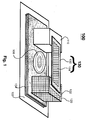
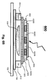
- FIGs. 6A and 6B illustrate a photon detector according to another exemplary embodiment of the invention.
- FIG. 6A is a schematic top perspective view of a photon detector (600)
- FIG. 6B is a schematic side view of the photon detector (600) taken along line 6B-6B in FIG. 6A .
- the photon detector (600) comprises a substrate (102), digital logic circuitry (104), a parabolic mirror (106), a bridge structure formed on the substrate (102).
- the bridge structure includes a first support member (610), a second support member (612), a third support member (614), a resonator member (620), an insulating layer (622), and a ribbon member (630).
- the resonator member (620) is connected between the second and third support members (612) and (614), wherein the resonator member (620) is suspended above the substrate (102) (which is in contrast to previously discussed embodiments in which the resonator member serves as a support member anchored to the substrate).
- the ribbon structure (630) comprise a bimetal layer (632) and a photon energy absorbing layer (634) (e.g., carbon, carbon nanotubes, SiC, etc.).
- the ribbon structure (630) is connected between the first support member (610) and the resonator member (620).
- the ribbon structure (630) comprises a plurality of tabs (632A, 632B, 632C and 632D) which are integrally formed as part of the bimetal layer (632), wherein the ribbon (630) is connected to the resonator member (620) via the tabs (632A, 632B, 632C and 632D).
- the tabs (632A, 632B, 632C and 632D) and the insulating layer (622) serve to thermally isolate the resonator member (620) from the bimetal layer (632).
- the second support member (612) provides supply voltage V+ to the resonator member (620) and the third support member (614) provides a ground connection for the resonator member (620).
- FIG. 7 is a perspective view of a visible light detector (700) framework according to an exemplary embodiment of the invention, which is based on the PICE concept.
- the detector (700) comprises a substrate (102), digital logic circuitry (104), and a bridge structure formed on the substrate (102).
- the bridge structure includes a first support member (710), a second support member (720) and a ribbon member (730) suspended between the support members (710) and (720) above the substrate (102).
- the support member (720) is a resonator member that operates at a resonant frequency and the second support member (710) is a fixed insulating support structure.
- the ribbon structure (730) is made from a photo-sensitive material (such as CdS, ZnO) having a photon induced coefficient of expansion, which causes mechanical deformation of the ribbon structure (7300 caused directly by photonic exposure.
- An insulating material layer (722) is disposed between the end of the ribbon (730) and the resonator member (720) to provide thermal and electrical isolation between the ribbon (730) and the resonator support structure (720).
- the ribbon structure (730) includes a layer of material (e.g., CdS) which receives incident photons, causing the ribbon (730) to stress and change length. This stress is transferred to the resonator (720), which causes it to change its resonant frequency in proportion to the amount of incident photon exposure.
- the digital logic circuit (104) is coupled to the resonator member (720) for determining a change in oscillating frequency of the resonator member (720) due to force exerted on the resonator member (720) by the mechanical expansion and contraction of the ribbon structure (730), wherein the change in frequency is correlated to an amount of incident photon energy received by the ribbon structure (730).
- FIGs. 8-14 are perspective views of various detector frameworks according to exemplary embodiments of the invention, which are based on the VID concept.
- These frameworks provide a passive detector architecture for wavelengths, X-rays (1nm) through Near IR (3 ⁇ ), wherein a ribbon material produces a voltage from photon exposure, and wherein the voltage is applied to a piezo material layer that will cause the material to distort and create the stress to alter the resonator frequency.
- a pyroelectric material may be used to generate a voltage that when applied to a piezo material layer will cause the material to distort and create the stress to alter the resonator frequency.
- FIG. 8 is a perspective view of a visible/UV light detector (800) framework according to an exemplary embodiment of the invention, which is based on the VID concept.
- the detector (800) comprises a substrate and digital logic circuitry (not specifically shown, but similar to all embodiments discussed above) and a bridge structure formed on the substrate 102.
- the bridge structure includes a first support member (810), a second support member (820) and a ribbon structure (830) suspended between the support members (810) and (820) above the substrate.
- the support member (820) is a resonator member that operates at a resonant frequency and the support member (810) is a fixed insulating support structure.
- the ribbon structure (830) comprises photon sensitive layer (832), an insulating layer (834), a piezoelectric layer (836) and connecting members (838) that provide electrical connections between layers (832) and (836).
- the photon sensitive layer (832) is made from a photo-sensitive material that generates a voltage from exposure to incident photons (visible light or UV radiation).
- the voltage generated by layer (8320 is transferred to the piezoelectric layer (836) via connections (838), wherein the piezoelectric layer (836) reacts to the voltage by creating stress as it tries to change its length.
- This stress is transferred to the resonator (820), which causes it to change its resonant frequency in proportion to the amount of incident photon exposure.
- the digital logic circuit coupled to the resonator member (820) determines a change in frequency of the resonant frequency of the resonator member (820) due to force exerted on the resonator member (820) by the mechanical expansion and contraction of the piezo layer (836), wherein the change in frequency is correlated to an amount of incident photon energy received by the ribbon structure (830).
- This framework operates on a photovoltaic effect.
- FIG. 9 is a perspective view of a detector (900) framework according to another exemplary embodiment of the invention, which is based on the VID concept.
- the detector (900) comprises a substrate and digital logic circuitry (not specifically shown, but similar to all embodiments discussed above) and a bridge structure formed on the substrate.
- the bridge structure includes a first support member (910), a second support member (920) and a ribbon structure (930) suspended between the support members (910) and (920) above the substrate.
- the support member (920) is a resonator member that operates at a resonant frequency and the support member (910) is a fixed insulating support structure.
- the ribbon structure (930) comprises an IR sensitive layer (932), an insulating layer (934), a piezoelectric layer (936) and connecting members (938) that provide electrical connections between layers (932) and (936).
- the IR sensitive layer (932) is made from a pyroelectric material that generates a voltage from exposure to incident IR radiation.
- the voltage generated by layer (932) is transferred to the piezoelectric layer (936) via connections (938), wherein the piezoelectric layer (936) reacts to the voltage by creating stress as it tries to change its length.
- This stress is transferred to the resonator (920), which causes it to change its resonant frequency in proportion to the amount of incident IR exposure.
- the digital logic circuit coupled to the resonator member (920) determines a change in the oscillating frequency of the resonator member (920) due to force exerted on the resonator member (920) by the mechanical expansion and contraction of the piezo layer (936), wherein the change in frequency is correlated to an amount of incident photon energy received by the ribbon structure (930).
- This framework operates on a pyroelectric effect to provide a detection structure for IR radiation.
- FIG. 10 is a perspective view of a detector (1000) framework according to another exemplary embodiment of the invention, which is based on the VID concept.
- the detector (100) comprises a substrate and digital logic circuitry (not specifically shown, but similar to all embodiments discussed above) and a bridge structure formed on the substrate.
- the bridge structure includes a first support member (1010), a second support member (1012) and a ribbon structure (1030) suspended between the support members (1010) and (1012) above the substrate.
- the support members (1010) and (1012) are both insulating members.
- the ribbon structure (1030) comprises an IR sensitive layer (1032) (pyroelectric layer), an insulating layer (1034), a piezoelectric layer (1036) connecting members (1038) that provide electrical connections between layers (1032) and (1036), a second insulating layer (1037) and a resonator member (1039).
- the IR sensitive layer (1032) is made from a pyroelectric material that generates a voltage from exposure to incident IR radiation. The voltage generated by layer (1032) is transferred to the piezoelectric layer (1036) via connections (1038), wherein the piezoelectric layer (1036) reacts to the voltage by creating stress as it tries to change its length.
- This stress is transferred to the resonator (1039), which is mechanically coupled to the piezoelectric layer (1036) via the second insulating layer (1037).
- the stress imparted on the resonator layer (1039) by the piezoelectric layer (1036) causes the resonator member (1039) to change its resonant frequency in proportion to the amount of incident IR exposure.
- the digital logic circuit coupled to the resonator member (1039) determines a change in the oscillating frequency of the resonator member (1039) due to force exerted on the resonator member (1039) by the mechanical expansion and contraction of the piezo layer (1036), wherein the change in frequency is correlated to an amount of incident photon energy received by the ribbon structure (1030).
- This framework operates on a pyroelectric effect to provide a detection structure for IR radiation.
- FIG. 11 is a perspective view of a detector (1100) framework according to another exemplary embodiment of the invention, which is based on the VID concept.
- the detector (1100) comprises a substrate and digital logic circuitry (not specifically shown, but similar to all embodiments discussed above) and a bridge structure formed on the substrate.
- the bridge structure includes a first support member (1110), a second support member (1120) and a ribbon structure (1130) suspended between the support members (1110) and (1120) above the substrate.
- An insulating layer (1122) is interposed between the ribbon structure (1130) and the support member (1120).
- the support member (1120) is a resonator member that operates at a resonant frequency and the support member (1110) is a fixed insulating support structure.
- the ribbon structure (1130) comprises an IR sensitive layer (1132), an insulating layer (1134), a piezoelectric layer (1136) and connecting members (1138) that provide electrical connections between layers (1132) and (1136).
- the IR sensitive layer (1132) is made from a pyroelectric material that generates a voltage from exposure to incident IR radiation.
- the voltage generated by layer (1132) is transferred to the piezoelectric layer (1136) via connections (1138), wherein the piezoelectric layer (1136) reacts to the voltage by creating stress as it tries to change its length. This stress is transferred to the resonator (1120), which causes it to change its resonant frequency in proportion to the amount of incident IR exposure.
- the framework and operation of the detector of FIG. 11 is similar to that of FIG. 9 , but where the ribbon structure (1130) of FIG. 11 is formed in an accordion or bellows shape. This shape increases the surface area exposed to the incident photons. The increased area allows for more heating in the thermal IR mode and to generate more voltage in the photoelectric mode, increasing the expansion characteristics.
- FIG. 12 is a perspective view of a detector (1200) framework according to another exemplary embodiment of the invention, which is based on the VID concept.
- the detector (1200) comprises a substrate and digital logic circuitry (not specifically shown, but similar to all embodiments discussed above) and a bridge structure formed on the substrate.
- the bridge structure includes a first support member (1210), a second support member (1212) and a ribbon structure (1230) suspended between the support members (1210) and (1212) above the substrate.
- the support members (1210) and (1212) are both insulating members.
- the ribbon structure (1230) comprises an IR sensitive layer (1232) (pyroelectric layer), an insulating layer (1234), a piezoelectric layer (1236) connecting members (1238) that provide electrical connections between layers (1232) and (1236), a second insulating layer (1237) and a resonator member (1239).
- the IR sensitive layer (1232) is made from a pyroelectric material that generates a voltage from exposure to incident IR radiation. The voltage generated by layer (1232) is transferred to the piezoelectric layer (1236) via connections (1238), wherein the piezoelectric layer (1236) reacts to the voltage by creating stress as it tries to change its length.
- This stress is transferred to the resonator (1239), which is mechanically coupled to the piezoelectric layer (1236) via the second insulating layer (1237).
- the stress imparted on the resonator layer (1239) by the piezoelectric layer (1236) causes the resonator member (1239) to change its resonant frequency in proportion to the amount of incident IR exposure.
- the framework and operation of the detector structure of FIG. 12 is similar to that of FIG. 10 , but where the ribbon structure (1230) of FIG. 12 is formed in an accordion or bellows shape. This shape increases the surface area exposed to the incident photons. The increased area allows for more heating in the thermal IR mode and to generate more voltage in the photoelectric mode, increasing the expansion characteristics.
- FIG. 13 schematically illustrates a top view (10) and a side view (12) of an accordion or bellows shaped ribbon structure, wherein the ribbon is made of a single material.
- FIG. 14 schematically illustrates a top view (16) and a side view (14) of an accordion or bellows shaped ribbon structure, wherein the ribbon is made of alternating materials A and B, which are different.
- the use of alternating materials on a photo sensitive/IR sensitive ribbon layer e.g., layers 1132, 1232) can provide sensitivity with better linearity or wider or different spectral wavelengths.
- alternating materials on a resonator or piezo ribbon layer allows for materials with different expansion coefficient characteristics to control detector response, improve stress linearity, resonator linearity, or allow for custom response characteristics.
- FIGs. 15A and 15B illustrate a photon detector (1500) according to another exemplary embodiment of the invention, which is based on a CTE framework.
- FIG. 15A is a top view of the photon detector (1500)
- FIG. 15B is a cross-sectional view of the photon detector (1500) taken along line 15B-15B in FIG. 15A .
- the photon detector (1500) comprises a substrate (1502), a first support member (1510), a second support member (1520), fixedly connected to the substrate (1502), and a plate member (1530) disposed between the first and second support members (1510) and (1520).
- a plate member (1530
- the first support member (1510) is a fixed insulating support structure and the second support member (1520) is a fixed resonator member that operates at a resonant frequency.
- the plate member (1530) is formed of one or more materials that are sensitive to IR energy, and having a thermal coefficient of expansion which causes the plate member (1530) to expand and contract by absorption of incident infrared energy to exert force on the resonator support member (1520).
- the first and second support members (1510) and (1520) include grooves that insertably receive opposing ends of the plate member (1530).
- the end portions of the plate member (1530) comprise supporting leg elements (1532) which serve to maintain the IR absorbing portion of the plate member (1530) at some offset height from the surface of the substrate (1502). This allows the plate member (1530) to be substantially thermally insulated from the substrate (1502).
- the plate member (1530) is disposed between the first and second support members (1510) and (1520) in a "pre-stressed” state.
- the end portions of the plate member (1530) within the grooves of the first and second support members (1510) and (1520) exert some minimal force against the inner surfaces of the first and second support members (1510) and (1520) in the absence of any IR exposure.
- pre-stressing the plate member (1530) between the first and second support members (1510) and (1520) serves many functions. For example, pre-stressing the end portions of the plate member (1530) against the inner side and top wall surfaces of the grooves prevents the plate member (1530) from moving out of position due to vibrations and camera movement.
- pre-stressing the plate member (1530) reduces or eliminates mechanical and vibration noise. Furthermore, pre-stressing the plate member (1530) against the resonator member (1520) eliminates fluctuations in data measurement due to non-uniform stress distribution. Pre-stressing the plate member (1530) enables immediate readings of ⁇ fo (change in oscillating frequency) of the resonator member (1520), which is cause by expansion of the plate member (1530) upon an increase in incident IR exposure on the plate member (1530).
- disposing the plate member (1530) between the first and second support members (1510) and (1520) in a "pre-stressed” state can be realized by dimensioning the various support and plate elements in a manner that the end portions of the plate member (1530) securely fit (wedged) within the grooves of the support members (1510) and (1520).
- a filler material may be used to fill any small gaps or spaces between the end portions of the plate member (1530) and the inner side and top wall surfaces of the grooves of the first and second support members (1510) and (1520).
- the filler material can be any suitable material that will not cause the end portions of the plate member (1530) to adhere to the substrate (1502) or the first and second support members (1510) and (1520), and which does not deteriorate due to thermal and mechanical conditions over repeated use and operation of the detector (1500).
- Teflon is one suitable material that can be used for this purpose.
- a digital logic circuit (not specifically shown) is coupled to the resonator member (1520) for determining a change in the oscillating frequency of the resonator member (1520) due to force exerted on the resonator member (1520) by the thermal expansion and contraction of the plate member (1530), wherein the change in frequency is correlated to an amount of incident infrared energy absorbed by the plate member (1530).
- the substrate (1502) can be made of materials such as silicon, glass, ceramic, etc.
- the size of each detector (pixel) can be about 40 um x 45 ⁇ m, with a pixel pitch of about 50 ⁇ m.
- the plate member (1530) can be made of materials or layers of different materials providing sufficient thermal expansion and thermal conductivity, such as Zn, Au, SiC (silicon carbide), ZnS (zinc selenide), BN (boron nitride), ZnO (zinc oxide), or Si3N4 (silicon nitride), etc.
- the thermally conductive plate materials can be fabricated to facilitate a larger direction of thermal conductivity in a direction beneficial to the design, wherein the larger conductivity direction is parallel to the direction of the grain created by the fabrication.
- the stress direction of the plate member (1530) can be in a direction along the substrate between the first and second support members (1510) and (1520) as determined by the grain structure of the plate member (1530) created during fabrication.
- the plate member (1530) can be coated with any suitable materials such as DLC, SiC, CaF2, etc., to enhance thermal IR absorption in the 4 ⁇ m and 10 ⁇ m spectrum, for example. These coating materials should have sufficient expansion and adhesive properties to prevent delamination over time.
- the resonator member (1520) may be made of materials such as Lead Zirconate Titanate (PZT), Lead Scandium Tantalate, Barium Strontium Titanate, Bismuth Sodium Titanate (BNT), Barium Titanate (MHz range).
- PZT Lead Zirconate Titanate
- BNT Bismuth Sodium Titanate
- the thermal and stress reaction time constants of the plate member (1530) should be made fast enough for standard or faster video frame rates. For instance, a rise and fall cycle time of ⁇ 2ms would be sufficient for frame rates of 30 frames per second.
- FIGs. 16A and 16B illustrate a photon detector according to another exemplary embodiment of the invention, which is based on a CTE framework.
- FIG. 16A is a cross-sectional view of the photon detector (1600) taken along line 16A-16A in FIG. 16B
- FIG. 16B is a top view of the photon detector (1600).
- the photon detector (1600) comprises a substrate (1602), a first support member (1610), a second support member (1620), a plate member (1630), and a resonator member (1640).
- the plate member (1630) is disposed between the first support member (1610) and the resonator member (1640).
- the first and second support members (1610) and (1620) are fixed insulating support structures.
- the resonator member (1640) operates at a resonant frequency.
- the plate member (1630) is formed of one or more materials that are sensitive to IR energy, and having a thermal coefficient of expansion which causes the plate member (1630) to expand and contract by absorption of incident infrared energy to exert force on the resonator member (1640).
- the first support member (1610) comprises a slot (1612) formed in a sidewall thereof.
- the second support member (1620) is formed of two separate support elements, including a first lower support element (1622) and a second upper support element (1624), which are fixedly disposed adjacent to, and in contact with, a sidewall of the resonator member (1640).
- the lower and upper support elements (1622) and (1624) are spaced apart to form a slot region (1626) there between.
- the plate member (1630) has one end inserted in the slot (1612) of the first support member (1610) and another end inserted in the slot (1626) formed by the lower and upper support elements (1622) and (1624).
- the first and second support members (1610) and (1620) maintain the plate member (1630) at some offset height from the surface of the substrate (1602), such that the plate member (1630) is completely thermally insulated from the substrate (1602).
- a digital logic circuit (not specifically shown) is coupled to the resonator member (1640) for determining a change in the oscillating frequency of the resonator member (1640) due to force exerted on the resonator member (1640) by the thermal expansion and contraction of the plate member (1630), wherein the change in frequency is correlated to an amount of incident infrared energy absorbed by the plate member (1630).
- the plates member (1630) can be disposed between the first support member (1610) and the resonator member (1640) in a "pre-stressed" state, for reasons discussed above.
- the various structures can be dimensioned such that the end portions of the plate member (1630) are securely fit (wedged) within the slots (1612) and (1626).
- a filler material may be used to fill any small gaps or spaces between the end portions of the plate member (1630) and the inner surfaces of the slots (1612) and (1626) and the sidewall of the resonator member (1640).
- FIGs. 17A and 17B illustrate a photon detector (1700) according to another exemplary embodiment of the invention, which is based on a CTE framework.
- FIG. 17A is a cross-sectional view of the photon detector (1700) taken along line 17A-17A in FIG. 17B
- FIG. 17B is a top view of the photon detector (1700) taken along line 17B-17B in FIG. 17A .
- the photon detector (1700) comprises a substrate (1702), a first support member (1710), a second support member (1720) disposed the substrate (1702), and a plate member (1730).
- the second support member (1720) is a rectangular-shaped resonator member having a cavity region (1722) formed in one surface thereof.
- An optional thin thermal insulating layer (not shown) may be disposed between the bottom surface of the resonator member (1720) and the surface of the substrate (1702).
- the plate member (1730) is disposed within the cavity region (1722) of the resonator member (1720).
- the plate member (1730) is secured in place in the cavity region (1722) by the first support member (1710).
- the first support member (1710) may be a continuous rectangular frame structure that is fixedly secured to the top surface of the resonator member (1720), wherein a portion of the first support member (1710) overlaps the inner sidewalls of the cavity region (1722) to provide a lip that covers the upper peripheral surface edge of the plate member (1730), while leaving a large surface area for the plate member (1730) to absorb incident IR energy.
- the first support member (1710) may comprise a plurality of separate elements that are disposed in certain regions around the perimeter of the cavity region (1722) (e.g., each sidewall corner, or at a midpoint along each sidewall, etc.) sufficient to maintain the plate member (1730) within the cavity region (1722).
- the plate member (1730) can be disposed within the cavity (1722) of the resonator member (1720) in a "pre-stressed" state, for reasons discussed above.
- the resonator member (1720) operates at a resonant frequency.
- the plate member (1730) is formed of one or more materials that are sensitive to IR energy, and having a thermal coefficient of expansion which causes the plate member (1730) to expand and contract by absorption of incident infrared energy to exert force on the resonator member (1720). In the exemplary embodiment of FIGs.
- the plate member (1730) expands in response to heating caused by absorption of incident infrared energy, the plate member (1730) exerts a force on the resonator member (1720) in three dimensions.
- the plate member (1730) exerts a first horizontal force (Fx) in the x-direction on a first pair of opposing inner sidewalls of the cavity region (1720) of the resonator member (1720), and a second horizontal force (Fy) in the y-direction on a second pair of opposing inner sidewalls of the cavity region (1722) of the resonator member (1720).
- the plate member (1730) exerts a vertical force (Fz) against a bottom surface of the cavity region (1722) of the resonator member (1720) as the plate member (1730) expands in the z-direction between the overlapping lip portion of the first support member (1710) and the bottom surface of the cavity region (1722).
- a vertical force Fz exerted against the bottom surface of the first support member elements (1710) will translate a vertical force to the top surface of the resonator member (1720) along the sidewalls (which define the cavity region (1722)).
- a digital logic circuit (not specifically shown) is coupled to the resonator member (1720) for determining a change in frequency of the resonant frequency of the resonator member (1720) due to force exerted on the resonator member (172) by the thermal expansion and contraction of the plate member (1720), wherein the change in frequency is correlated to an amount of incident infrared energy absorbed by the plate member (1630).
- the sensitivity of the detector is increased as the change in frequency of the resonant frequency of the resonator member (1720) is due to stresses applied to the resonator member (1720) in three (x-y-z) dimensions.
- the detector framework is passive, i.e., the detector elements (e.g., CTE ribbons, CTE plates) are not part of the active electrical circuit.
- the detector elements e.g., CTE ribbons, CTE plates
- FIG. 18 is a graphical illustration (20) showing an advantage of using a direct-to-digital passive detector frameworks over conventional analog signal detector or quantum electronic designs, according to exemplary embodiments of the invention.
- FIG. 18 illustrates electrical noise (26) that can mask or interfere with an analog signal (22) containing desired sensor data, which is lost in noise (24). In order for the signal data to be detected, it must be greater than noise level (or 'noise floor') (26).
- An analog signal (22) as shown in FIG. 18 is susceptible to noise because small changes in the signal data may be smaller in amplitude than the systems noise level or noise floor, which masks that part of the analog signal (so it is lost). This is a major limiting factor to any systems overall sensitivity and performance.
- the analog signal (22) can be converted to a series of binary numbers (logic 1 and logic 0). These binary numbers are represented by square waves (23) that modulate between the systems voltage low point and high point. To be detected, the square waves need only switch above or below the system transition level (21) to be valid data. Digital design enable acquisition of valid data by using the leading or falling edge of the square wave signal.
- FIG. 19 is a block diagram of an imager system implementing passive detectors, according to an exemplary embodiment of the invention.
- FIG. 19 shows an imager circuit comprising a pixel structure (50), pixel circuitry (60), a read out integrated circuit (70) ("ROIC"), a controller (80), and an image rendering system (90).
- the pixel (50) comprises a passive detector front-end structure (52) and a resonator structure (54).
- the pixel circuitry (60) comprises a digital counter (62) and a tri-state register (64).
- the controller (80) comprises a counter enable/hold control block (81), a register reset block (82), an ROIC control block (83), a data input control block (84), and a video output control block (85).
- the passive detector front-end structure (52) generically represents any one of the passive pixel detector structures discussed herein, including the support structures and detector elements (e.g., CTE ribbons, plates structures, etc.) that are designed to be mechanically distorted in response to photon exposure, for example, and apply mechanical stress (force) to the resonator structure (54).
- the detector front-end structure (54) is electrically passive and has no noise generating electronics.
- the resonator structure (54) oscillates at a resonant frequency F o and outputs a square wave signal.
- the resonator structure (54) is designed to have a reference (or base) resonant frequency (no photon exposure) in a state in which no additional stress, other than the prestress amount, is applied to the resonator structure (54) by the detector front-end (52) due to photon exposure.
- the oscillating frequency of the resonator member (54) will increase from its reference (base) resonant frequency.
- the digital circuits (60), (70) and (80) collectively operate to determine the output frequency F o of the resonator member (54) due to the force exerted on the resonator member (54) by the expansion and contraction of a passive detector element (e.g., ribbon, plate) of the detector front end structure (52), determine an amount of incident photonic energy absorbed by the passive detector element based on the determined resonant frequency F o of the resonator member (54) at a given time, and generate image data based on the determined amount of incident photonic energy at the given time, which is then rendered by the imaging system (90).
- a passive detector element e.g., ribbon, plate
- the output signal generated by the resonator member (54) is a digital square wave signal having a frequency F o that varies depending on the stress applied to the resonator member (54) by the passive detector front-end structure (52).
- the output signal generated by the resonator member (54) is input to a clock input port of the digital counter (62).
- the digital counter (62) For each read cycle (or frame) of the imager, the digital counter (62) counts the pulses of the output signal from the resonator member (54) for a given "counting period" (or reference period) of the read cycle.
- the counting operation of the digital counter (62) is controlled by a CLK enable signal generated by the counter control block (81) of the controller (80).
- the count information generated by the counter (62) is output as an n-bit count value to the tri-state register (64).
- the ROIC 70 reads out the count value (pixel data) from the pixel circuitry (60) of a given pixel (50) for each read cycle. It is to be understood that for ease of illustration, FIG. 19 shows one pixel unit (50) and one corresponding pixel circuit (60), but an imager can have a plurality of pixel units (50) and corresponding pixel circuits (60) forming a linear pixel array or a 2D focal plane pixel array, for example.
- the ROIC (70) is connected to each pixel circuit (60) over a shared n-bit data bus (66), for controllably transferring the individual pixel data from the each pixel counting circuit (60) (which is preferably formed in the active silicon substrate surface under each corresponding pixel structure (50)) to the controller (80).
- the ROIC (70) in response to control signals received from the ROIC control block (83) of the controller (80), the ROIC (70) will output a tri-state control signal to the pixel circuitry (60) of a given pixel (50) to read out the stored count data in the shift-register (64) onto the shared data bus (66).
- the shift-register (64) of each pixel circuit (60) is individually controlled by the ROIC (70) to obtain the count data for each pixel at a time over the data bus (66).
- the count data is transferred from the ROIC (70) to the controller (80) over a dedicated data bus (72) connected to the n-bit data input control block (84) of the controller (80).
- the tri-state register (64) of each pixel will be reset via a control signal output from the register reset control block (82) of the controller (80).
- the controller (80) processes the count data obtained from each pixel in each read cycle (or video frame) to determine the amount of incident photon exposure for each pixel and uses the determined exposure data to create a video image.
- the video data is output to an image rendering system (90) via the video output block (85) to display an image.
- the controller (80) will use the count data to determine a grayscale level for the pixel, which corresponds to the amount of the incident photonic exposure of the pixel.
- the grayscale level can be determined using a grayscale algorithm or using a lookup table in which the different grayscale values (over a range from black to white) are correlated with a range of count values for a priori determined increments of changes in the oscillating frequency of the resonator member from the base reference frequency to a maximum oscillating frequency.
- the maximum oscillating frequency is the highest frequency that can output from the resonator member in response to the maximum amount of stress force that can be created by the given passive detector front-end structure.
- the pixel structure and pixel circuitry of FIG. 19 can be modified such that the counter will count the frequency of a signal that represents the difference between the base resonant frequency of the resonator member (54) and the actual output frequency generated by the resonator member (54) at a given time in response to stress applied by the passive detector front-end (52).
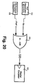
- FIG. 20 illustrates another exemplary embodiment of a pixel unit and pixel circuitry that can be implemented in the imager system of FIG. 19 .
- the pixel (50) (of FIG. 19 ) is modified to include a reference oscillator (56) that outputs a reference resonant frequency F ref .
- the 19 is modified to include an exclusive-Or gate (66) that receives as input, the output signal of the resonator member (54) (having a variable frequency Fo) and the fixed signal from the reference oscillator (56).
- the X-Or gate (66) operates to remove the base frequency component of the signal Fo output from the resonator member (54) based on the reference frequency of the reference oscillator (56) and outputs a square wave signal having a frequency equal to the change ⁇ F o in frequency of resonator member (54).
- the ⁇ F o frequency signal which is much lower in frequency than the oscillating frequency Fo of the resonator member (54), requires a lower bit number counter (62) to count the ⁇ F o signal, making it simpler to implement.
- the ⁇ F o signal is counted for a reference period and the count value is used to determine incident photon exposure of the pixel, as discussed above.
Landscapes
- Physics & Mathematics (AREA)
- General Physics & Mathematics (AREA)
- Spectroscopy & Molecular Physics (AREA)
- Chemical & Material Sciences (AREA)
- Engineering & Computer Science (AREA)
- Crystallography & Structural Chemistry (AREA)
- Power Engineering (AREA)
- Nanotechnology (AREA)
- Photometry And Measurement Of Optical Pulse Characteristics (AREA)
- Transforming Light Signals Into Electric Signals (AREA)
- Radiation Pyrometers (AREA)
- Spectrometry And Color Measurement (AREA)
Claims (16)
- Un dispositif d'imagerie, comprenant :un substrat,un détecteur à infrarouge thermique formé sur le substrat, où le détecteur à infrarouge thermique comprend :un élément résonateur piézoélectrique formé d'un matériau piézoélectrique qui est configuré de façon à résonner en réponse à une tension d'attaque et à générer un signal en sortie possédant une fréquence ou une période d'oscillation,un élément détecteur non alimenté électriquement, où l'élément détecteur non alimenté électriquement est configuré pour une exposition à un rayonnement infrarouge thermique incident, où l'élément détecteur non alimenté électriquement contient un matériau possédant un coefficient d'expansion thermique qui amène l'élément détecteur non alimenté électriquement à se déformer du fait de l'absorption dudit rayonnement infrarouge thermique incident, où l'élément détecteur non alimenté électriquement est configuré en outre de façon à appliquer une force mécanique à l'élément résonateur piézoélectrique du fait de ladite distorsion de l'élément détecteur non alimenté électriquement, et à amener une modification dans la fréquence ou la période d'oscillation du signal en sortie généré par l'élément résonateur piézoélectrique du fait de ladite force mécanique appliquée à l'élément résonateur piézoélectrique, etun élément d'isolation thermique configuré de façon à isoler thermiquement l'élément résonateur piézoélectrique de l'élément détecteur non alimenté électriquement, etun circuit numérique configuré de façon à (i) déterminer la fréquence ou la période d'oscillation du signal en sortie généré par l'élément résonateur piézoélectrique en conséquence de la force mécanique appliquée à l'élément résonateur piézoélectrique par l'élément détecteur non alimenté électriquement, et de façon à (ii) déterminer une quantité de ladite exposition à un rayonnement infrarouge thermique incident en fonction de la fréquence ou de la période d'oscillation déterminée du signal en sortie généré par l'élément résonateur piézoélectrique.
- Le dispositif d'imagerie selon la Revendication 1, où le dispositif d'imagerie est configuré de façon à détecter une énergie infrarouge thermique possédant une longueur d'onde dans une plage d'environ 1 micromètre à 30 micromètres.
- Le dispositif d'imagerie selon la Revendication 1, où l'élément d'isolation thermique comprend une couche de matériau d'isolation thermique disposée entre l'élément résonateur piézoélectrique et l'élément détecteur non alimenté électriquement.
- Le dispositif d'imagerie selon la Revendication 1, comprenant en outre un premier élément support, où l'élément détecteur non alimenté électriquement comprend un élément plaque, et où l'élément plaque est disposé entre le premier élément support et l'élément résonateur piézoélectrique, où l'élément plaque contient un matériau possédant un coefficient d'expansion thermique qui amène l'élément plaque à se déformer du fait de l'absorption dudit rayonnement infrarouge thermique incident et à appliquer ladite force mécanique à l'élément résonateur piézoélectrique.
- Le dispositif d'imagerie selon la Revendication 4, où le premier élément support possède une première rainure et où l'élément résonateur piézoélectrique comprend un deuxième rainure, où des extrémités de l'élément plaque sont disposées à l'intérieur des première et deuxième rainures.
- Le dispositif d'imagerie selon la Revendication 4, comprenant en outre un deuxième élément support, disposé adjacent à l'élément résonateur piézoélectrique, où le premier élément support possède une première rainure et où le deuxième élément support possède une deuxième rainure, où des extrémités de l'élément plaque sont disposées à l'intérieur des première et deuxième rainures, où la deuxième rainure permet à l'élément plaque d'appliquer ladite force mécanique à l'élément résonateur piézoélectrique à mesure que l'élément plaque se déforme du fait de l'absorption dudit rayonnement infrarouge thermique incident.
- Le dispositif d'imagerie selon la Revendication 4, où l'élément plaque est disposé entre le premier élément support et l'élément résonateur piézoélectrique dans un état précontraint.
- Le dispositif d'imagerie selon la Revendication 1, où l'élément résonateur piézoélectrique comprend une zone de cavité encastrée formée dans une surface de l'élément résonateur piézoélectrique, où l'élément détecteur non alimenté électriquement comprend un élément plaque qui est disposé à l'intérieur de la zone de cavité encastrée de l'élément résonateur piézoélectrique, où la structure de détecteur passive comprend en outre un premier élément support qui est disposé sur la surface de l'élément résonateur piézoélectrique et qui chevauche au moins une partie de la zone de cavité encastrée de façon à fixer l'élément plaque à l'intérieur de la zone de cavité, et où l'élément plaque contient un matériau possédant un coefficient d'expansion thermique qui amène l'élément plaque à se déformer du fait de l'absorption dudit rayonnement infrarouge thermique incident et à appliquer ladite force mécanique à l'élément résonateur piézoélectrique.
- Le dispositif d'imagerie selon la Revendication 8, où le premier élément support est une structure de châssis continue qui est fixée de manière fixe à la surface de l'élément résonateur piézoélectrique, où une partie du premier élément support chevauche les parois latérales intérieures de la zone de cavité de façon à fournir une lèvre qui recouvre un bord de surface périphérique supérieur de l'élément plaque, tout en laissant une zone de surface ouverte à l'élément plaque destinée à l'absorption dudit rayonnement infrarouge thermique incident.
- Le dispositif d'imagerie selon la Revendication 8, où une distorsion de l'élément plaque amène ladite force mécanique à être appliquée à l'élément résonateur piézoélectrique en trois dimensions,
- Le dispositif d'imagerie selon la Revendication 8, où l'élément plaque est disposé à l'intérieur de la cavité encastrée de l'élément résonateur piézoélectrique dans un état précontraint.
- Le dispositif d'imagerie selon la Revendication 1, où le détecteur à infrarouge thermique comprend en outre une première électrode et une deuxième électrode, où l'élément résonateur piézoélectrique est raccordé à et entre les première et deuxième électrodes et est suspendu au-dessus d'une surface du substrat, et où les première et deuxième électrodes appliquent la tension d'attaque à l'élément résonateur piézoélectrique.
- Le dispositif d'imagerie selon la Revendication 12, où le détecteur à infrarouge thermique comprend en outre un élément support fixe raccordé au substrat, où une première extrémité de l'élément détecteur non alimenté électriquement est couplée mécaniquement à l'élément support fixe et où une deuxième extrémité de l'élément détecteur non alimenté électriquement est couplée mécaniquement à l'élément résonateur piézoélectrique.
- Un procédé d'imagerie, comprenant :l'exposition d'un détecteur à infrarouge thermique à un rayonnement infrarouge thermique incident, le détecteur à infrarouge thermique comprenant un élément détecteur non alimenté électriquement, un élément résonateur piézoélectrique et un élément d'isolation thermique configuré de façon à isoler thermiquement l'élément résonateur piézoélectrique de l'élément détecteur non alimenté électriquement, où l'élément résonateur piézoélectrique est formé d'un matériau piézoélectrique qui est configuré de façon à résonner en réponse à une tension d'attaque et à générer un signal en sortie possédant une fréquence ou une période d'oscillation,la déformation de l'élément détecteur non alimenté électriquement du fait de ladite exposition à un rayonnement infrarouge thermique incident, où l'élément détecteur non alimenté électriquement contient un matériau possédant un coefficient d'expansion thermique qui amène l'élément détecteur non alimenté électriquement à se déformer du fait de l'absorption dudit rayonnement infrarouge thermique incident,l'application d'une force mécanique à l'élément résonateur piézoélectrique du fait de la déformation de l'élément détecteur non alimenté électriquement,la détermination d'une fréquence ou d'une période d'oscillation du signal en sortie généré par l'élément résonateur piézoélectrique en conséquence de la force mécanique appliquée à l'élément résonateur piézoélectrique par l'élément détecteur non alimenté électriquement, etla détermination d'une quantité de ladite exposition à un rayonnement infrarouge thermique incident dudit détecteur à infrarouge thermique en fonction de ladite fréquence ou de ladite période d'oscillation déterminée du signal en sortie généré par l'élément résonateur piézoélectrique.
- Le procédé selon la Revendication 14, comprenant en outre la génération de données d'image au moyen de la fréquence déterminée.
- Le procédé selon la Revendication 14, où la détermination d'une quantité de ladite exposition à un rayonnement infrarouge thermique incident dudit détecteur à infrarouge thermique comprend :la génération de données de décompte par le décompte d'un nombre d'impulsions numériques dans le signal en sortie généré par l'élément résonateur piézoélectrique pour une période de décompte donnée, etla détermination d'un niveau d'exposition à un rayonnement infrarouge thermique incident en fonction desdites données de décompte.
Applications Claiming Priority (2)
| Application Number | Priority Date | Filing Date | Title |
|---|---|---|---|
| US201161524669P | 2011-08-17 | 2011-08-17 | |
| PCT/US2012/051376 WO2013026006A2 (fr) | 2011-08-17 | 2012-08-17 | Détecteurs passifs pour systèmes d'imagerie |
Publications (3)
| Publication Number | Publication Date |
|---|---|
| EP2745096A2 EP2745096A2 (fr) | 2014-06-25 |
| EP2745096A4 EP2745096A4 (fr) | 2015-07-22 |
| EP2745096B1 true EP2745096B1 (fr) | 2016-10-12 |
Family
ID=47715715
Family Applications (1)
| Application Number | Title | Priority Date | Filing Date |
|---|---|---|---|
| EP12823481.2A Not-in-force EP2745096B1 (fr) | 2011-08-17 | 2012-08-17 | Détecteurs passifs pour systèmes d'imagerie |
Country Status (6)
| Country | Link |
|---|---|
| US (5) | US9012845B2 (fr) |
| EP (1) | EP2745096B1 (fr) |
| JP (1) | JP6336904B2 (fr) |
| CN (1) | CN104040725B (fr) |
| IL (1) | IL230895B (fr) |
| WO (1) | WO2013026006A2 (fr) |
Families Citing this family (21)
| Publication number | Priority date | Publication date | Assignee | Title |
|---|---|---|---|---|
| US9097578B2 (en) * | 2011-05-13 | 2015-08-04 | The Regents Of The University Of Michigan | Infrared sensing using pyro/piezo-electric resonators |
| EP2745096B1 (fr) * | 2011-08-17 | 2016-10-12 | Public Service Solutions Inc | Détecteurs passifs pour systèmes d'imagerie |
| JP6245036B2 (ja) * | 2014-03-31 | 2017-12-13 | Tdk株式会社 | 赤外線検知装置 |
| WO2016069960A1 (fr) * | 2014-10-29 | 2016-05-06 | Digital Direct Ir Inc. | Réseaux sphériques de détecteurs réalisés à l'aide de structures de détecteurs passifs pour des applications d'imagerie thermique |
| US20170237911A1 (en) * | 2014-11-06 | 2017-08-17 | Siliconfile Technologies Inc. | Image sensor having improved spectral characteristics |
| US10948349B2 (en) * | 2015-04-14 | 2021-03-16 | Digital Direct Ir, Inc. | Multi-spectrum imaging |
| US10171758B2 (en) * | 2015-04-14 | 2019-01-01 | Digital Direct Ir, Inc. | Multi-spectrum imaging |
| US10168221B2 (en) * | 2016-03-18 | 2019-01-01 | Board Of Trustees Of The University Of Illinois | Uncooled, high sensitivity spectral selective infrared detector |
| EP3450935B1 (fr) * | 2016-04-28 | 2024-07-03 | Chuo University | Dispositif de détection d'ondes térahertz et capteur à barrettes |
| US10154207B2 (en) * | 2017-02-07 | 2018-12-11 | Sensors Unlimited, Inc. | Event-triggered imaging pixels |
| JP6892105B2 (ja) * | 2017-03-02 | 2021-06-18 | 国立大学法人 東京大学 | テラヘルツ波検出装置 |
| US10175113B2 (en) | 2017-04-12 | 2019-01-08 | Raytheon Company | Thermal protection mechanisms for uncooled microbolometers |
| US10288487B2 (en) * | 2017-08-10 | 2019-05-14 | Honeywell International Inc. | Apparatus and method for MEMS resonant sensor arrays |
| KR102008720B1 (ko) * | 2017-11-16 | 2019-08-09 | 한국생산기술연구원 | 탄소나노섬유 감지막을 구비한 적외선 센서 및 이를 이용한 적외선 센싱 방법 |
| US11019316B1 (en) * | 2018-02-09 | 2021-05-25 | Tdone, Llc | Sequential spectral imaging |
| US11029512B2 (en) * | 2018-06-27 | 2021-06-08 | Microsoft Technology Licensing, Llc | Adjusting a resonant frequency of a scanning mirror |
| CN111551251B (zh) * | 2019-02-11 | 2024-06-25 | Tdone有限公司 | 有序光谱成像 |
| US11552204B2 (en) * | 2019-04-03 | 2023-01-10 | Ohio State Innovation Foundation | Photonic detector coupled with a dielectric resonator antenna |
| KR102574448B1 (ko) * | 2020-08-26 | 2023-09-01 | 연세대학교 산학협력단 | 광반응성 복합 소재를 이용한 미세 전자 기계 시스템 기반 정전식 감응 센서 및 이의 센싱 방법 |
| CN113720455A (zh) * | 2021-03-26 | 2021-11-30 | 北京北方高业科技有限公司 | 基于cmos工艺的红外探测器 |
| TWI897815B (zh) * | 2025-02-26 | 2025-09-11 | 國立臺灣大學 | 具有光偵測元件陣列的偵測裝置 |
Family Cites Families (91)
| Publication number | Priority date | Publication date | Assignee | Title |
|---|---|---|---|---|
| US4069434A (en) | 1974-12-27 | 1978-01-17 | Kabushiki Kaisha Suwa Seikosha | Quartz crystal oscillator |
| US4060729A (en) | 1976-12-10 | 1977-11-29 | Martin Marietta Corporation | Pyroelectric detector with decreased susceptibility to vibrational noise |
| JPS5434286A (en) * | 1977-08-22 | 1979-03-13 | Ricoh Co Ltd | Light quantity display device |
| EP0048689B1 (fr) | 1980-08-29 | 1985-01-30 | Asulab S.A. | Thermomètre à quartz |
| US4459042A (en) | 1980-11-28 | 1984-07-10 | Novex, Inc. | Vibratory digital temperature sensor |
| US4592663A (en) | 1984-05-10 | 1986-06-03 | Quartex, Inc. | Resonator temperature transducer |
| US4897541A (en) | 1984-05-18 | 1990-01-30 | Luxtron Corporation | Sensors for detecting electromagnetic parameters utilizing resonating elements |
| GB2187551B (en) | 1986-03-04 | 1990-03-14 | Gen Electric Plc | Radiation detector |
| US5300915A (en) | 1986-07-16 | 1994-04-05 | Honeywell Inc. | Thermal sensor |
| US5336854A (en) | 1992-04-03 | 1994-08-09 | Weigh-Tronix, Inc. | Electronic force sensing load cell |
| JPH0783756A (ja) * | 1993-09-10 | 1995-03-31 | Semiconductor Res Found | 振動型赤外線センサ、振動型赤外線イメージャ、及び赤外線検出方法 |
| US7123216B1 (en) | 1994-05-05 | 2006-10-17 | Idc, Llc | Photonic MEMS and structures |
| US5686779A (en) | 1995-03-01 | 1997-11-11 | The United States Of America As Represented By The Secretary Of The Army | High sensitivity temperature sensor and sensor array |
| US5719324A (en) | 1995-06-16 | 1998-02-17 | Lockheed Martin Energy Systems, Inc. | Microcantilever sensor |
| US6118124A (en) | 1996-01-18 | 2000-09-12 | Lockheed Martin Energy Research Corporation | Electromagnetic and nuclear radiation detector using micromechanical sensors |
| US5844238A (en) | 1996-03-27 | 1998-12-01 | David Sarnoff Research Center, Inc. | Infrared imager using room temperature capacitance sensor |
| US5811807A (en) * | 1996-07-19 | 1998-09-22 | Ail Systems, Inc. | Uncooled background limited detector and method |
| US5747804A (en) | 1996-09-13 | 1998-05-05 | Raytheon Company | Method and apparatus for sensing infrared radiation utilizing a micro-electro-mechanical sensor |
| US6080988A (en) | 1996-12-20 | 2000-06-27 | Nikon Corporation | Optically readable radiation-displacement-conversion devices and methods, and image-rendering apparatus and methods employing same |
| US5917272A (en) | 1998-06-11 | 1999-06-29 | Vectron, Inc. | Oven-heated crystal resonator and oscillator assembly |
| US6809515B1 (en) | 1998-07-31 | 2004-10-26 | Spinix Corporation | Passive solid-state magnetic field sensors and applications therefor |
| US6805839B2 (en) | 1999-03-12 | 2004-10-19 | Joseph P. Cunningham | Response microcantilever thermal detector |
| US6525310B2 (en) | 1999-08-05 | 2003-02-25 | Microvision, Inc. | Frequency tunable resonant scanner |
| US6384406B1 (en) | 1999-08-05 | 2002-05-07 | Microvision, Inc. | Active tuning of a torsional resonant structure |
| WO2003007049A1 (fr) | 1999-10-05 | 2003-01-23 | Iridigm Display Corporation | Mems et structures photoniques |
| US6236145B1 (en) | 2000-02-29 | 2001-05-22 | Cts Corporation | High thermal resistivity crystal resonator support structure and oscillator package |
| GB0007325D0 (en) | 2000-03-27 | 2000-05-17 | Atherton Eric | High temperature sensor |
| US6828557B2 (en) | 2000-06-08 | 2004-12-07 | Nikon Corporation | Radiation-detection devices |
| WO2001099098A2 (fr) | 2000-06-19 | 2001-12-27 | Brigham Young University | Microactionneur thermo-mecanique en plan |
| US6392233B1 (en) | 2000-08-10 | 2002-05-21 | Sarnoff Corporation | Optomechanical radiant energy detector |
| US6739190B2 (en) | 2000-08-24 | 2004-05-25 | The Regents Of The University Of Michigan | Micromechanical resonator device |
| JP3409848B2 (ja) | 2000-08-29 | 2003-05-26 | 日本電気株式会社 | 熱型赤外線検出器 |
| JP4945861B2 (ja) | 2000-09-05 | 2012-06-06 | 株式会社ニコン | 熱型変位素子及びこれを用いた放射検出装置 |
| US20020074897A1 (en) | 2000-12-15 | 2002-06-20 | Qing Ma | Micro-electromechanical structure resonator frequency adjustment using radient energy trimming and laser/focused ion beam assisted deposition |
| US6457360B1 (en) | 2001-02-21 | 2002-10-01 | Conel Ltd. | High-precision integrated semiconductor peizoresistive detector devices and methods using the same |
| US6489616B2 (en) | 2001-03-19 | 2002-12-03 | The Board Of Governors Of Southwest Missouri State University | Doped, organic carbon-containing sensor for infrared detection and a process for the preparation thereof |
| US7026602B2 (en) | 2001-04-13 | 2006-04-11 | Research Triangle Institute | Electromagnetic radiation detectors having a microelectromechanical shutter device |
| JP2003106895A (ja) | 2001-10-01 | 2003-04-09 | Nec Corp | 熱型赤外線検出素子及びその製造方法 |
| US6744338B2 (en) | 2001-11-13 | 2004-06-01 | International Business Machines Corporation | Resonant operation of MEMS switch |
| JP2003185496A (ja) | 2001-12-13 | 2003-07-03 | Mitsubishi Electric Corp | 赤外線検出アレイおよびその製造方法 |
| JP4008258B2 (ja) | 2002-02-15 | 2007-11-14 | セイコーインスツル株式会社 | 圧電振動子の製造方法 |
| US6908201B2 (en) | 2002-06-28 | 2005-06-21 | Silicon Light Machines Corporation | Micro-support structures |
| US7057795B2 (en) | 2002-08-20 | 2006-06-06 | Silicon Light Machines Corporation | Micro-structures with individually addressable ribbon pairs |
| US6888141B2 (en) | 2002-12-02 | 2005-05-03 | Multispectral Imaging, Inc. | Radiation sensor with photo-thermal gain |
| JP2006518846A (ja) | 2003-02-05 | 2006-08-17 | ブルーネル ユニバーシティ | 共振センサーアセンブリー |
| US6922272B1 (en) | 2003-02-14 | 2005-07-26 | Silicon Light Machines Corporation | Method and apparatus for leveling thermal stress variations in multi-layer MEMS devices |
| US7434476B2 (en) | 2003-05-07 | 2008-10-14 | Califronia Institute Of Technology | Metallic thin film piezoresistive transduction in micromechanical and nanomechanical devices and its application in self-sensing SPM probes |
| GB0315526D0 (en) * | 2003-07-03 | 2003-08-06 | Qinetiq Ltd | Thermal detector |
| US7068125B2 (en) | 2004-03-04 | 2006-06-27 | Robert Bosch Gmbh | Temperature controlled MEMS resonator and method for controlling resonator frequency |
| US7161730B2 (en) | 2004-09-27 | 2007-01-09 | Idc, Llc | System and method for providing thermal compensation for an interferometric modulator display |
| US7566942B2 (en) | 2004-10-20 | 2009-07-28 | Massachusetts Institute Of Technology | Multi-spectral pixel and focal plane array |
| US7280078B2 (en) | 2004-11-20 | 2007-10-09 | Scenterra, Inc. | Sensor for detecting high frequency signals |
| TWI283739B (en) | 2004-12-28 | 2007-07-11 | Delta Electronics Inc | FBAR-based sensing apparatus |
| US7324323B2 (en) | 2005-01-13 | 2008-01-29 | Lucent Technologies Inc. | Photo-sensitive MEMS structure |
| US20060158484A1 (en) | 2005-01-14 | 2006-07-20 | Greywall Dennis S | Thermal actuator for a MEMS device |
| US7042230B1 (en) | 2005-02-28 | 2006-05-09 | Alain Izadnegahdar | Multi-parameter sensing system |
| WO2006119200A2 (fr) | 2005-04-29 | 2006-11-09 | The Board Of Trustees Of The Leland Stanford Junior University | Detecteur acoustique et optique compatible avec des fibres et presentant une sensibilite elevee |
| US7492241B2 (en) | 2005-06-02 | 2009-02-17 | The Regents Of The University Of California | Contour-mode piezoelectric micromechanical resonators |
| US7402803B1 (en) | 2005-06-07 | 2008-07-22 | Redshift Systems Corporation | Pixel architecture for thermal imaging system |
| US7637149B2 (en) | 2005-06-17 | 2009-12-29 | Georgia Tech Research Corporation | Integrated displacement sensors for probe microscopy and force spectroscopy |
| US7227432B2 (en) | 2005-06-30 | 2007-06-05 | Robert Bosch Gmbh | MEMS resonator array structure and method of operating and using same |
| WO2008048212A2 (fr) | 2005-07-07 | 2008-04-24 | The Regents Of The University Of California | Systèmes et dispositifs de capteur infrarouge |
| US7408147B2 (en) | 2005-07-27 | 2008-08-05 | Wisconsin Alumni Research Foundation | Nanoelectromechanical and microelectromechanical sensors and analyzers |
| WO2007037926A2 (fr) | 2005-09-23 | 2007-04-05 | Sharp Laboratories Of America, Inc. | Capteur de pixels mems |
| US7470920B2 (en) | 2006-01-05 | 2008-12-30 | Virgin Islands Microsystems, Inc. | Resonant structure-based display |
| US7495199B2 (en) | 2006-02-10 | 2009-02-24 | Stmicroelectronics, Inc. | MEMS radiometer |
| US7558490B2 (en) | 2006-04-10 | 2009-07-07 | Virgin Islands Microsystems, Inc. | Resonant detector for optical signals |
| US7442940B2 (en) | 2006-05-05 | 2008-10-28 | Virgin Island Microsystems, Inc. | Focal plane array incorporating ultra-small resonant structures |
| JP5384331B2 (ja) | 2006-06-01 | 2014-01-08 | ユニベルシテ・ド・リエージュ | 表面プラズモン共鳴に基づくセンサ |
| US7584649B2 (en) | 2006-06-02 | 2009-09-08 | Board Of Trustees Of Michigan State University | Sensor with microelectro-mechanical oscillators |
| US7667369B2 (en) | 2006-11-01 | 2010-02-23 | Delaware Capital Formation, Inc. | High sensitivity microsensors based on flexure induced frequency effects |
| WO2008112764A1 (fr) | 2007-03-12 | 2008-09-18 | Nantero, Inc. | Capteurs électromagnétiques et thermiques utilisant des nanotubes en carbone et procédés de fabrication de ceux-ci |
| US7956517B1 (en) * | 2007-05-10 | 2011-06-07 | Silicon Laboratories | MEMS structure having a stress inverter temperature-compensated resonator member |
| US8001830B2 (en) * | 2007-05-15 | 2011-08-23 | Anasys Instruments, Inc. | High frequency deflection measurement of IR absorption |
| US8402819B2 (en) * | 2007-05-15 | 2013-03-26 | Anasys Instruments, Inc. | High frequency deflection measurement of IR absorption |
| US7586239B1 (en) | 2007-06-06 | 2009-09-08 | Rf Micro Devices, Inc. | MEMS vibrating structure using a single-crystal piezoelectric thin film layer |
| US7580175B2 (en) * | 2007-06-21 | 2009-08-25 | Alcatel-Lucent Usa Inc. | Detector of infrared radiation having a bi-material transducer |
| EP2141490B1 (fr) | 2008-07-02 | 2015-04-01 | Stichting IMEC Nederland | Dispositif capteur chimique avec un microcantilever |
| JP4840451B2 (ja) | 2009-01-22 | 2011-12-21 | 住友電気工業株式会社 | 近赤外イメージセンサ |
| JP5523727B2 (ja) * | 2009-03-31 | 2014-06-18 | 学校法人トヨタ学園 | ねじり振動を利用した赤外線の検出方法とこれを実施したねじり振動を利用した赤外線センサ |
| US9121771B2 (en) | 2010-03-16 | 2015-09-01 | The Penn State Research Foundation | Methods and apparatus for ultra-sensitive temperature detection using resonant devices |
| US9097578B2 (en) * | 2011-05-13 | 2015-08-04 | The Regents Of The University Of Michigan | Infrared sensing using pyro/piezo-electric resonators |
| US9739667B2 (en) * | 2011-08-17 | 2017-08-22 | Digital Direct Ir, Inc. | Passive detectors for imaging systems |
| US20170023406A1 (en) * | 2011-08-17 | 2017-01-26 | Digital Direct Ir, Inc. | Passive detectors for imaging systems |
| EP2745096B1 (fr) * | 2011-08-17 | 2016-10-12 | Public Service Solutions Inc | Détecteurs passifs pour systèmes d'imagerie |
| JP6377153B2 (ja) * | 2013-06-25 | 2018-08-22 | デジタルダイレクト・アイアール、インク | サイドスキャン赤外線撮像装置 |
| WO2016069960A1 (fr) * | 2014-10-29 | 2016-05-06 | Digital Direct Ir Inc. | Réseaux sphériques de détecteurs réalisés à l'aide de structures de détecteurs passifs pour des applications d'imagerie thermique |
| US10948349B2 (en) * | 2015-04-14 | 2021-03-16 | Digital Direct Ir, Inc. | Multi-spectrum imaging |
| US10171758B2 (en) * | 2015-04-14 | 2019-01-01 | Digital Direct Ir, Inc. | Multi-spectrum imaging |
| US11165390B2 (en) * | 2015-06-12 | 2021-11-02 | Daishinku Corporation | Piezoelectric resonator device |
| CN109155620B (zh) * | 2016-06-29 | 2022-05-03 | 株式会社大真空 | 压电振动器件及压电振动器件的制造方法 |
-
2012
- 2012-08-17 EP EP12823481.2A patent/EP2745096B1/fr not_active Not-in-force
- 2012-08-17 JP JP2014526248A patent/JP6336904B2/ja not_active Expired - Fee Related
- 2012-08-17 WO PCT/US2012/051376 patent/WO2013026006A2/fr not_active Ceased
- 2012-08-17 US US13/588,441 patent/US9012845B2/en active Active
- 2012-08-17 CN CN201280051175.4A patent/CN104040725B/zh not_active Expired - Fee Related
-
2014
- 2014-02-10 IL IL230895A patent/IL230895B/en active IP Right Grant
-
2015
- 2015-04-02 US US14/677,954 patent/US9523612B2/en not_active Expired - Fee Related
-
2016
- 2016-12-19 US US15/383,779 patent/US10247614B2/en active Active
-
2019
- 2019-04-01 US US16/372,322 patent/US11105685B2/en not_active Expired - Fee Related
-
2021
- 2021-08-31 US US17/462,039 patent/US20220146324A1/en not_active Abandoned
Also Published As
| Publication number | Publication date |
|---|---|
| IL230895B (en) | 2018-03-29 |
| US9523612B2 (en) | 2016-12-20 |
| IL230895A0 (en) | 2014-03-31 |
| US10247614B2 (en) | 2019-04-02 |
| WO2013026006A3 (fr) | 2014-05-08 |
| US20130214158A1 (en) | 2013-08-22 |
| US11105685B2 (en) | 2021-08-31 |
| CN104040725A (zh) | 2014-09-10 |
| US20220146324A1 (en) | 2022-05-12 |
| JP2014524579A (ja) | 2014-09-22 |
| US20200096392A1 (en) | 2020-03-26 |
| US20170343420A1 (en) | 2017-11-30 |
| EP2745096A2 (fr) | 2014-06-25 |
| CN104040725B (zh) | 2017-08-22 |
| US20160047693A1 (en) | 2016-02-18 |
| WO2013026006A2 (fr) | 2013-02-21 |
| JP6336904B2 (ja) | 2018-06-06 |
| EP2745096A4 (fr) | 2015-07-22 |
| US9012845B2 (en) | 2015-04-21 |
Similar Documents
| Publication | Publication Date | Title |
|---|---|---|
| EP2745096B1 (fr) | Détecteurs passifs pour systèmes d'imagerie | |
| US8143577B2 (en) | Infrared sensors, focal plane arrays and thermal imaging systems | |
| US20150321905A1 (en) | Wafer level packaged infrared (ir) focal plane array (fpa) with evanescent wave coupling | |
| CN102874735B (zh) | 双材料微悬臂梁、电磁辐射探测器以及探测方法 | |
| CN101063630A (zh) | 一种基于微桥谐振器的红外探测器结构及制作方法 | |
| US20100084556A1 (en) | Optical-infrared composite sensor and method of fabricating the same | |
| CN202924718U (zh) | 双材料微悬臂梁、电磁辐射探测器 | |
| JP2000298062A (ja) | 熱型機能デバイス、エネルギー検出装置および熱型機能デバイスの駆動方法 | |
| CA3226086A1 (fr) | Detecteurs de microbolometres avec cavites resonantes pour absorption optique amelioree | |
| US9897488B2 (en) | Vibration based mechanical IR detector and an IR imaging method using the same | |
| US11035735B2 (en) | Spherical detector arrays implemented using passive detector structures for thermal imaging applications | |
| US7842923B2 (en) | Thermal actuator for an infrared sensor | |
| US9658110B1 (en) | Thermal sensor combination | |
| EP2005127A1 (fr) | Détecteurs de lumière en porte-à-faux | |
| Rogalski | Novel uncooled infrared detectors | |
| CN103630246A (zh) | 一种非制冷红外成像焦平面阵列探测器 | |
| CN101498608A (zh) | 带自支撑框架的全镂空结构光调制热成像焦平面阵列 |
Legal Events
| Date | Code | Title | Description |
|---|---|---|---|
| PUAI | Public reference made under article 153(3) epc to a published international application that has entered the european phase |
Free format text: ORIGINAL CODE: 0009012 |
|
| 17P | Request for examination filed |
Effective date: 20140313 |
|
| AK | Designated contracting states |
Kind code of ref document: A2 Designated state(s): AL AT BE BG CH CY CZ DE DK EE ES FI FR GB GR HR HU IE IS IT LI LT LU LV MC MK MT NL NO PL PT RO RS SE SI SK SM TR |
|
| R17P | Request for examination filed (corrected) |
Effective date: 20141104 |
|
| DAX | Request for extension of the european patent (deleted) | ||
| A4 | Supplementary search report drawn up and despatched |
Effective date: 20150623 |
|
| RIC1 | Information provided on ipc code assigned before grant |
Ipc: G01J 5/04 20060101ALI20150617BHEP Ipc: G01N 21/27 20060101AFI20150617BHEP Ipc: H01J 37/22 20060101ALI20150617BHEP Ipc: G01J 5/02 20060101ALI20150617BHEP |
|
| RIC1 | Information provided on ipc code assigned before grant |
Ipc: G01J 5/02 20060101ALI20160128BHEP Ipc: G01N 21/27 20060101AFI20160128BHEP Ipc: G01J 5/04 20060101ALI20160128BHEP Ipc: G01J 5/44 20060101ALI20160128BHEP Ipc: H01J 37/22 20060101ALI20160128BHEP Ipc: G01J 5/34 20060101ALI20160128BHEP |
|
| GRAP | Despatch of communication of intention to grant a patent |
Free format text: ORIGINAL CODE: EPIDOSNIGR1 |
|
| INTG | Intention to grant announced |
Effective date: 20160307 |
|
| GRAS | Grant fee paid |
Free format text: ORIGINAL CODE: EPIDOSNIGR3 |
|
| GRAA | (expected) grant |
Free format text: ORIGINAL CODE: 0009210 |
|
| AK | Designated contracting states |
Kind code of ref document: B1 Designated state(s): AL AT BE BG CH CY CZ DE DK EE ES FI FR GB GR HR HU IE IS IT LI LT LU LV MC MK MT NL NO PL PT RO RS SE SI SK SM TR |
|
| REG | Reference to a national code |
Ref country code: GB Ref legal event code: FG4D |
|
| REG | Reference to a national code |
Ref country code: CH Ref legal event code: EP |
|
| REG | Reference to a national code |
Ref country code: AT Ref legal event code: REF Ref document number: 836962 Country of ref document: AT Kind code of ref document: T Effective date: 20161015 |
|
| REG | Reference to a national code |
Ref country code: IE Ref legal event code: FG4D |
|
| REG | Reference to a national code |
Ref country code: DE Ref legal event code: R096 Ref document number: 602012024149 Country of ref document: DE |
|
| REG | Reference to a national code |
Ref country code: LT Ref legal event code: MG4D |
|
| REG | Reference to a national code |
Ref country code: NL Ref legal event code: MP Effective date: 20161012 |
|
| PG25 | Lapsed in a contracting state [announced via postgrant information from national office to epo] |
Ref country code: LV Free format text: LAPSE BECAUSE OF FAILURE TO SUBMIT A TRANSLATION OF THE DESCRIPTION OR TO PAY THE FEE WITHIN THE PRESCRIBED TIME-LIMIT Effective date: 20161012 |
|
| REG | Reference to a national code |
Ref country code: AT Ref legal event code: MK05 Ref document number: 836962 Country of ref document: AT Kind code of ref document: T Effective date: 20161012 |
|
| PG25 | Lapsed in a contracting state [announced via postgrant information from national office to epo] |
Ref country code: SE Free format text: LAPSE BECAUSE OF FAILURE TO SUBMIT A TRANSLATION OF THE DESCRIPTION OR TO PAY THE FEE WITHIN THE PRESCRIBED TIME-LIMIT Effective date: 20161012 Ref country code: LT Free format text: LAPSE BECAUSE OF FAILURE TO SUBMIT A TRANSLATION OF THE DESCRIPTION OR TO PAY THE FEE WITHIN THE PRESCRIBED TIME-LIMIT Effective date: 20161012 Ref country code: NO Free format text: LAPSE BECAUSE OF FAILURE TO SUBMIT A TRANSLATION OF THE DESCRIPTION OR TO PAY THE FEE WITHIN THE PRESCRIBED TIME-LIMIT Effective date: 20170112 Ref country code: GR Free format text: LAPSE BECAUSE OF FAILURE TO SUBMIT A TRANSLATION OF THE DESCRIPTION OR TO PAY THE FEE WITHIN THE PRESCRIBED TIME-LIMIT Effective date: 20170113 |
|
| PG25 | Lapsed in a contracting state [announced via postgrant information from national office to epo] |
Ref country code: BE Free format text: LAPSE BECAUSE OF FAILURE TO SUBMIT A TRANSLATION OF THE DESCRIPTION OR TO PAY THE FEE WITHIN THE PRESCRIBED TIME-LIMIT Effective date: 20161012 Ref country code: ES Free format text: LAPSE BECAUSE OF FAILURE TO SUBMIT A TRANSLATION OF THE DESCRIPTION OR TO PAY THE FEE WITHIN THE PRESCRIBED TIME-LIMIT Effective date: 20161012 Ref country code: AT Free format text: LAPSE BECAUSE OF FAILURE TO SUBMIT A TRANSLATION OF THE DESCRIPTION OR TO PAY THE FEE WITHIN THE PRESCRIBED TIME-LIMIT Effective date: 20161012 Ref country code: PT Free format text: LAPSE BECAUSE OF FAILURE TO SUBMIT A TRANSLATION OF THE DESCRIPTION OR TO PAY THE FEE WITHIN THE PRESCRIBED TIME-LIMIT Effective date: 20170213 Ref country code: RS Free format text: LAPSE BECAUSE OF FAILURE TO SUBMIT A TRANSLATION OF THE DESCRIPTION OR TO PAY THE FEE WITHIN THE PRESCRIBED TIME-LIMIT Effective date: 20161012 Ref country code: HR Free format text: LAPSE BECAUSE OF FAILURE TO SUBMIT A TRANSLATION OF THE DESCRIPTION OR TO PAY THE FEE WITHIN THE PRESCRIBED TIME-LIMIT Effective date: 20161012 Ref country code: NL Free format text: LAPSE BECAUSE OF FAILURE TO SUBMIT A TRANSLATION OF THE DESCRIPTION OR TO PAY THE FEE WITHIN THE PRESCRIBED TIME-LIMIT Effective date: 20161012 Ref country code: FI Free format text: LAPSE BECAUSE OF FAILURE TO SUBMIT A TRANSLATION OF THE DESCRIPTION OR TO PAY THE FEE WITHIN THE PRESCRIBED TIME-LIMIT Effective date: 20161012 Ref country code: IS Free format text: LAPSE BECAUSE OF FAILURE TO SUBMIT A TRANSLATION OF THE DESCRIPTION OR TO PAY THE FEE WITHIN THE PRESCRIBED TIME-LIMIT Effective date: 20170212 Ref country code: PL Free format text: LAPSE BECAUSE OF FAILURE TO SUBMIT A TRANSLATION OF THE DESCRIPTION OR TO PAY THE FEE WITHIN THE PRESCRIBED TIME-LIMIT Effective date: 20161012 |
|
| REG | Reference to a national code |
Ref country code: DE Ref legal event code: R097 Ref document number: 602012024149 Country of ref document: DE |
|
| PG25 | Lapsed in a contracting state [announced via postgrant information from national office to epo] |
Ref country code: SK Free format text: LAPSE BECAUSE OF FAILURE TO SUBMIT A TRANSLATION OF THE DESCRIPTION OR TO PAY THE FEE WITHIN THE PRESCRIBED TIME-LIMIT Effective date: 20161012 Ref country code: EE Free format text: LAPSE BECAUSE OF FAILURE TO SUBMIT A TRANSLATION OF THE DESCRIPTION OR TO PAY THE FEE WITHIN THE PRESCRIBED TIME-LIMIT Effective date: 20161012 Ref country code: RO Free format text: LAPSE BECAUSE OF FAILURE TO SUBMIT A TRANSLATION OF THE DESCRIPTION OR TO PAY THE FEE WITHIN THE PRESCRIBED TIME-LIMIT Effective date: 20161012 Ref country code: CZ Free format text: LAPSE BECAUSE OF FAILURE TO SUBMIT A TRANSLATION OF THE DESCRIPTION OR TO PAY THE FEE WITHIN THE PRESCRIBED TIME-LIMIT Effective date: 20161012 Ref country code: DK Free format text: LAPSE BECAUSE OF FAILURE TO SUBMIT A TRANSLATION OF THE DESCRIPTION OR TO PAY THE FEE WITHIN THE PRESCRIBED TIME-LIMIT Effective date: 20161012 |
|
| PLBE | No opposition filed within time limit |
Free format text: ORIGINAL CODE: 0009261 |
|
| STAA | Information on the status of an ep patent application or granted ep patent |
Free format text: STATUS: NO OPPOSITION FILED WITHIN TIME LIMIT |
|
| PG25 | Lapsed in a contracting state [announced via postgrant information from national office to epo] |
Ref country code: SM Free format text: LAPSE BECAUSE OF FAILURE TO SUBMIT A TRANSLATION OF THE DESCRIPTION OR TO PAY THE FEE WITHIN THE PRESCRIBED TIME-LIMIT Effective date: 20161012 Ref country code: IT Free format text: LAPSE BECAUSE OF FAILURE TO SUBMIT A TRANSLATION OF THE DESCRIPTION OR TO PAY THE FEE WITHIN THE PRESCRIBED TIME-LIMIT Effective date: 20161012 Ref country code: BG Free format text: LAPSE BECAUSE OF FAILURE TO SUBMIT A TRANSLATION OF THE DESCRIPTION OR TO PAY THE FEE WITHIN THE PRESCRIBED TIME-LIMIT Effective date: 20170112 |
|
| 26N | No opposition filed |
Effective date: 20170713 |
|
| PG25 | Lapsed in a contracting state [announced via postgrant information from national office to epo] |
Ref country code: SI Free format text: LAPSE BECAUSE OF FAILURE TO SUBMIT A TRANSLATION OF THE DESCRIPTION OR TO PAY THE FEE WITHIN THE PRESCRIBED TIME-LIMIT Effective date: 20161012 |
|
| REG | Reference to a national code |
Ref country code: FR Ref legal event code: PLFP Year of fee payment: 6 |
|
| REG | Reference to a national code |
Ref country code: CH Ref legal event code: PL |
|
| PG25 | Lapsed in a contracting state [announced via postgrant information from national office to epo] |
Ref country code: MC Free format text: LAPSE BECAUSE OF FAILURE TO SUBMIT A TRANSLATION OF THE DESCRIPTION OR TO PAY THE FEE WITHIN THE PRESCRIBED TIME-LIMIT Effective date: 20161012 |
|
| PG25 | Lapsed in a contracting state [announced via postgrant information from national office to epo] |
Ref country code: CH Free format text: LAPSE BECAUSE OF NON-PAYMENT OF DUE FEES Effective date: 20170831 Ref country code: LI Free format text: LAPSE BECAUSE OF NON-PAYMENT OF DUE FEES Effective date: 20170831 |
|
| REG | Reference to a national code |
Ref country code: IE Ref legal event code: MM4A |
|
| PG25 | Lapsed in a contracting state [announced via postgrant information from national office to epo] |
Ref country code: LU Free format text: LAPSE BECAUSE OF NON-PAYMENT OF DUE FEES Effective date: 20170817 |
|
| PG25 | Lapsed in a contracting state [announced via postgrant information from national office to epo] |
Ref country code: IE Free format text: LAPSE BECAUSE OF NON-PAYMENT OF DUE FEES Effective date: 20170817 |
|
| REG | Reference to a national code |
Ref country code: FR Ref legal event code: PLFP Year of fee payment: 7 |
|
| PG25 | Lapsed in a contracting state [announced via postgrant information from national office to epo] |
Ref country code: MT Free format text: LAPSE BECAUSE OF NON-PAYMENT OF DUE FEES Effective date: 20170817 |
|
| PG25 | Lapsed in a contracting state [announced via postgrant information from national office to epo] |
Ref country code: HU Free format text: LAPSE BECAUSE OF FAILURE TO SUBMIT A TRANSLATION OF THE DESCRIPTION OR TO PAY THE FEE WITHIN THE PRESCRIBED TIME-LIMIT; INVALID AB INITIO Effective date: 20120817 |
|
| PG25 | Lapsed in a contracting state [announced via postgrant information from national office to epo] |
Ref country code: CY Free format text: LAPSE BECAUSE OF NON-PAYMENT OF DUE FEES Effective date: 20161012 |
|
| PG25 | Lapsed in a contracting state [announced via postgrant information from national office to epo] |
Ref country code: MK Free format text: LAPSE BECAUSE OF FAILURE TO SUBMIT A TRANSLATION OF THE DESCRIPTION OR TO PAY THE FEE WITHIN THE PRESCRIBED TIME-LIMIT Effective date: 20161012 |
|
| PG25 | Lapsed in a contracting state [announced via postgrant information from national office to epo] |
Ref country code: TR Free format text: LAPSE BECAUSE OF FAILURE TO SUBMIT A TRANSLATION OF THE DESCRIPTION OR TO PAY THE FEE WITHIN THE PRESCRIBED TIME-LIMIT Effective date: 20161012 |
|
| PG25 | Lapsed in a contracting state [announced via postgrant information from national office to epo] |
Ref country code: AL Free format text: LAPSE BECAUSE OF FAILURE TO SUBMIT A TRANSLATION OF THE DESCRIPTION OR TO PAY THE FEE WITHIN THE PRESCRIBED TIME-LIMIT Effective date: 20161012 |
|
| PGFP | Annual fee paid to national office [announced via postgrant information from national office to epo] |
Ref country code: GB Payment date: 20220824 Year of fee payment: 11 Ref country code: DE Payment date: 20220825 Year of fee payment: 11 |
|
| PGFP | Annual fee paid to national office [announced via postgrant information from national office to epo] |
Ref country code: FR Payment date: 20220823 Year of fee payment: 11 |
|
| REG | Reference to a national code |
Ref country code: DE Ref legal event code: R119 Ref document number: 602012024149 Country of ref document: DE |
|
| GBPC | Gb: european patent ceased through non-payment of renewal fee |
Effective date: 20230817 |
|
| PG25 | Lapsed in a contracting state [announced via postgrant information from national office to epo] |
Ref country code: GB Free format text: LAPSE BECAUSE OF NON-PAYMENT OF DUE FEES Effective date: 20230817 |
|
| PG25 | Lapsed in a contracting state [announced via postgrant information from national office to epo] |
Ref country code: GB Free format text: LAPSE BECAUSE OF NON-PAYMENT OF DUE FEES Effective date: 20230817 Ref country code: FR Free format text: LAPSE BECAUSE OF NON-PAYMENT OF DUE FEES Effective date: 20230831 Ref country code: DE Free format text: LAPSE BECAUSE OF NON-PAYMENT OF DUE FEES Effective date: 20240301 |