EP2748867B1 - Dispositif électrochromique à oxyde conducteur transparent nanostructuré - Google Patents
Dispositif électrochromique à oxyde conducteur transparent nanostructuré Download PDFInfo
- Publication number
- EP2748867B1 EP2748867B1 EP12828240.7A EP12828240A EP2748867B1 EP 2748867 B1 EP2748867 B1 EP 2748867B1 EP 12828240 A EP12828240 A EP 12828240A EP 2748867 B1 EP2748867 B1 EP 2748867B1
- Authority
- EP
- European Patent Office
- Prior art keywords
- nanostructures
- electrochromic
- substrate
- film
- wavelength
- Prior art date
- Legal status (The legal status is an assumption and is not a legal conclusion. Google has not performed a legal analysis and makes no representation as to the accuracy of the status listed.)
- Active
Links
Images








Classifications
-
- G—PHYSICS
- G02—OPTICS
- G02F—OPTICAL DEVICES OR ARRANGEMENTS FOR THE CONTROL OF LIGHT BY MODIFICATION OF THE OPTICAL PROPERTIES OF THE MEDIA OF THE ELEMENTS INVOLVED THEREIN; NON-LINEAR OPTICS; FREQUENCY-CHANGING OF LIGHT; OPTICAL LOGIC ELEMENTS; OPTICAL ANALOGUE/DIGITAL CONVERTERS
- G02F1/00—Devices or arrangements for the control of the intensity, colour, phase, polarisation or direction of light arriving from an independent light source, e.g. switching, gating or modulating; Non-linear optics
- G02F1/01—Devices or arrangements for the control of the intensity, colour, phase, polarisation or direction of light arriving from an independent light source, e.g. switching, gating or modulating; Non-linear optics for the control of the intensity, phase, polarisation or colour
- G02F1/15—Devices or arrangements for the control of the intensity, colour, phase, polarisation or direction of light arriving from an independent light source, e.g. switching, gating or modulating; Non-linear optics for the control of the intensity, phase, polarisation or colour based on an electrochromic effect
- G02F1/153—Constructional details
- G02F1/155—Electrodes
-
- B—PERFORMING OPERATIONS; TRANSPORTING
- B82—NANOTECHNOLOGY
- B82Y—SPECIFIC USES OR APPLICATIONS OF NANOSTRUCTURES; MEASUREMENT OR ANALYSIS OF NANOSTRUCTURES; MANUFACTURE OR TREATMENT OF NANOSTRUCTURES
- B82Y20/00—Nanooptics, e.g. quantum optics or photonic crystals
-
- E—FIXED CONSTRUCTIONS
- E06—DOORS, WINDOWS, SHUTTERS, OR ROLLER BLINDS IN GENERAL; LADDERS
- E06B—FIXED OR MOVABLE CLOSURES FOR OPENINGS IN BUILDINGS, VEHICLES, FENCES OR LIKE ENCLOSURES IN GENERAL, e.g. DOORS, WINDOWS, BLINDS, GATES
- E06B9/00—Screening or protective devices for wall or similar openings, with or without operating or securing mechanisms; Closures of similar construction
- E06B9/24—Screens or other constructions affording protection against light, especially against sunshine; Similar screens for privacy or appearance; Slat blinds
-
- G—PHYSICS
- G02—OPTICS
- G02F—OPTICAL DEVICES OR ARRANGEMENTS FOR THE CONTROL OF LIGHT BY MODIFICATION OF THE OPTICAL PROPERTIES OF THE MEDIA OF THE ELEMENTS INVOLVED THEREIN; NON-LINEAR OPTICS; FREQUENCY-CHANGING OF LIGHT; OPTICAL LOGIC ELEMENTS; OPTICAL ANALOGUE/DIGITAL CONVERTERS
- G02F1/00—Devices or arrangements for the control of the intensity, colour, phase, polarisation or direction of light arriving from an independent light source, e.g. switching, gating or modulating; Non-linear optics
- G02F1/01—Devices or arrangements for the control of the intensity, colour, phase, polarisation or direction of light arriving from an independent light source, e.g. switching, gating or modulating; Non-linear optics for the control of the intensity, phase, polarisation or colour
- G02F1/15—Devices or arrangements for the control of the intensity, colour, phase, polarisation or direction of light arriving from an independent light source, e.g. switching, gating or modulating; Non-linear optics for the control of the intensity, phase, polarisation or colour based on an electrochromic effect
- G02F1/1514—Devices or arrangements for the control of the intensity, colour, phase, polarisation or direction of light arriving from an independent light source, e.g. switching, gating or modulating; Non-linear optics for the control of the intensity, phase, polarisation or colour based on an electrochromic effect characterised by the electrochromic material, e.g. by the electrodeposited material
- G02F1/1523—Devices or arrangements for the control of the intensity, colour, phase, polarisation or direction of light arriving from an independent light source, e.g. switching, gating or modulating; Non-linear optics for the control of the intensity, phase, polarisation or colour based on an electrochromic effect characterised by the electrochromic material, e.g. by the electrodeposited material comprising inorganic material
-
- G—PHYSICS
- G02—OPTICS
- G02F—OPTICAL DEVICES OR ARRANGEMENTS FOR THE CONTROL OF LIGHT BY MODIFICATION OF THE OPTICAL PROPERTIES OF THE MEDIA OF THE ELEMENTS INVOLVED THEREIN; NON-LINEAR OPTICS; FREQUENCY-CHANGING OF LIGHT; OPTICAL LOGIC ELEMENTS; OPTICAL ANALOGUE/DIGITAL CONVERTERS
- G02F1/00—Devices or arrangements for the control of the intensity, colour, phase, polarisation or direction of light arriving from an independent light source, e.g. switching, gating or modulating; Non-linear optics
- G02F1/01—Devices or arrangements for the control of the intensity, colour, phase, polarisation or direction of light arriving from an independent light source, e.g. switching, gating or modulating; Non-linear optics for the control of the intensity, phase, polarisation or colour
- G02F1/15—Devices or arrangements for the control of the intensity, colour, phase, polarisation or direction of light arriving from an independent light source, e.g. switching, gating or modulating; Non-linear optics for the control of the intensity, phase, polarisation or colour based on an electrochromic effect
- G02F1/163—Operation of electrochromic cells, e.g. electrodeposition cells; Circuit arrangements therefor
-
- E—FIXED CONSTRUCTIONS
- E06—DOORS, WINDOWS, SHUTTERS, OR ROLLER BLINDS IN GENERAL; LADDERS
- E06B—FIXED OR MOVABLE CLOSURES FOR OPENINGS IN BUILDINGS, VEHICLES, FENCES OR LIKE ENCLOSURES IN GENERAL, e.g. DOORS, WINDOWS, BLINDS, GATES
- E06B9/00—Screening or protective devices for wall or similar openings, with or without operating or securing mechanisms; Closures of similar construction
- E06B9/24—Screens or other constructions affording protection against light, especially against sunshine; Similar screens for privacy or appearance; Slat blinds
- E06B2009/2405—Areas of differing opacity for light transmission control
-
- E—FIXED CONSTRUCTIONS
- E06—DOORS, WINDOWS, SHUTTERS, OR ROLLER BLINDS IN GENERAL; LADDERS
- E06B—FIXED OR MOVABLE CLOSURES FOR OPENINGS IN BUILDINGS, VEHICLES, FENCES OR LIKE ENCLOSURES IN GENERAL, e.g. DOORS, WINDOWS, BLINDS, GATES
- E06B9/00—Screening or protective devices for wall or similar openings, with or without operating or securing mechanisms; Closures of similar construction
- E06B9/24—Screens or other constructions affording protection against light, especially against sunshine; Similar screens for privacy or appearance; Slat blinds
- E06B2009/2464—Screens or other constructions affording protection against light, especially against sunshine; Similar screens for privacy or appearance; Slat blinds featuring transparency control by applying voltage, e.g. LCD, electrochromic panels
-
- G—PHYSICS
- G02—OPTICS
- G02F—OPTICAL DEVICES OR ARRANGEMENTS FOR THE CONTROL OF LIGHT BY MODIFICATION OF THE OPTICAL PROPERTIES OF THE MEDIA OF THE ELEMENTS INVOLVED THEREIN; NON-LINEAR OPTICS; FREQUENCY-CHANGING OF LIGHT; OPTICAL LOGIC ELEMENTS; OPTICAL ANALOGUE/DIGITAL CONVERTERS
- G02F1/00—Devices or arrangements for the control of the intensity, colour, phase, polarisation or direction of light arriving from an independent light source, e.g. switching, gating or modulating; Non-linear optics
- G02F1/01—Devices or arrangements for the control of the intensity, colour, phase, polarisation or direction of light arriving from an independent light source, e.g. switching, gating or modulating; Non-linear optics for the control of the intensity, phase, polarisation or colour
- G02F1/15—Devices or arrangements for the control of the intensity, colour, phase, polarisation or direction of light arriving from an independent light source, e.g. switching, gating or modulating; Non-linear optics for the control of the intensity, phase, polarisation or colour based on an electrochromic effect
- G02F1/153—Constructional details
- G02F1/155—Electrodes
- G02F2001/1555—Counter electrode
-
- G—PHYSICS
- G02—OPTICS
- G02F—OPTICAL DEVICES OR ARRANGEMENTS FOR THE CONTROL OF LIGHT BY MODIFICATION OF THE OPTICAL PROPERTIES OF THE MEDIA OF THE ELEMENTS INVOLVED THEREIN; NON-LINEAR OPTICS; FREQUENCY-CHANGING OF LIGHT; OPTICAL LOGIC ELEMENTS; OPTICAL ANALOGUE/DIGITAL CONVERTERS
- G02F1/00—Devices or arrangements for the control of the intensity, colour, phase, polarisation or direction of light arriving from an independent light source, e.g. switching, gating or modulating; Non-linear optics
- G02F1/01—Devices or arrangements for the control of the intensity, colour, phase, polarisation or direction of light arriving from an independent light source, e.g. switching, gating or modulating; Non-linear optics for the control of the intensity, phase, polarisation or colour
- G02F1/15—Devices or arrangements for the control of the intensity, colour, phase, polarisation or direction of light arriving from an independent light source, e.g. switching, gating or modulating; Non-linear optics for the control of the intensity, phase, polarisation or colour based on an electrochromic effect
- G02F2001/164—Devices or arrangements for the control of the intensity, colour, phase, polarisation or direction of light arriving from an independent light source, e.g. switching, gating or modulating; Non-linear optics for the control of the intensity, phase, polarisation or colour based on an electrochromic effect the electrolyte is made of polymers
-
- G—PHYSICS
- G02—OPTICS
- G02F—OPTICAL DEVICES OR ARRANGEMENTS FOR THE CONTROL OF LIGHT BY MODIFICATION OF THE OPTICAL PROPERTIES OF THE MEDIA OF THE ELEMENTS INVOLVED THEREIN; NON-LINEAR OPTICS; FREQUENCY-CHANGING OF LIGHT; OPTICAL LOGIC ELEMENTS; OPTICAL ANALOGUE/DIGITAL CONVERTERS
- G02F2202/00—Materials and properties
- G02F2202/36—Micro- or nanomaterials
-
- G—PHYSICS
- G02—OPTICS
- G02F—OPTICAL DEVICES OR ARRANGEMENTS FOR THE CONTROL OF LIGHT BY MODIFICATION OF THE OPTICAL PROPERTIES OF THE MEDIA OF THE ELEMENTS INVOLVED THEREIN; NON-LINEAR OPTICS; FREQUENCY-CHANGING OF LIGHT; OPTICAL LOGIC ELEMENTS; OPTICAL ANALOGUE/DIGITAL CONVERTERS
- G02F2203/00—Function characteristic
- G02F2203/10—Function characteristic plasmon
-
- G—PHYSICS
- G02—OPTICS
- G02F—OPTICAL DEVICES OR ARRANGEMENTS FOR THE CONTROL OF LIGHT BY MODIFICATION OF THE OPTICAL PROPERTIES OF THE MEDIA OF THE ELEMENTS INVOLVED THEREIN; NON-LINEAR OPTICS; FREQUENCY-CHANGING OF LIGHT; OPTICAL LOGIC ELEMENTS; OPTICAL ANALOGUE/DIGITAL CONVERTERS
- G02F2203/00—Function characteristic
- G02F2203/11—Function characteristic involving infrared radiation
-
- Y—GENERAL TAGGING OF NEW TECHNOLOGICAL DEVELOPMENTS; GENERAL TAGGING OF CROSS-SECTIONAL TECHNOLOGIES SPANNING OVER SEVERAL SECTIONS OF THE IPC; TECHNICAL SUBJECTS COVERED BY FORMER USPC CROSS-REFERENCE ART COLLECTIONS [XRACs] AND DIGESTS
- Y10—TECHNICAL SUBJECTS COVERED BY FORMER USPC
- Y10S—TECHNICAL SUBJECTS COVERED BY FORMER USPC CROSS-REFERENCE ART COLLECTIONS [XRACs] AND DIGESTS
- Y10S977/00—Nanotechnology
- Y10S977/70—Nanostructure
- Y10S977/762—Nanowire or quantum wire, i.e. axially elongated structure having two dimensions of 100 nm or less
-
- Y—GENERAL TAGGING OF NEW TECHNOLOGICAL DEVELOPMENTS; GENERAL TAGGING OF CROSS-SECTIONAL TECHNOLOGIES SPANNING OVER SEVERAL SECTIONS OF THE IPC; TECHNICAL SUBJECTS COVERED BY FORMER USPC CROSS-REFERENCE ART COLLECTIONS [XRACs] AND DIGESTS
- Y10—TECHNICAL SUBJECTS COVERED BY FORMER USPC
- Y10S—TECHNICAL SUBJECTS COVERED BY FORMER USPC CROSS-REFERENCE ART COLLECTIONS [XRACs] AND DIGESTS
- Y10S977/00—Nanotechnology
- Y10S977/902—Specified use of nanostructure
- Y10S977/932—Specified use of nanostructure for electronic or optoelectronic application
Definitions
- Embodiments described herein relate to the field of electroehromics, and particularly relate to a nanostructured transparent conducting oxide electrochromic device.
- WO20137016318 which is a document cited under Art. 54(3) EPC, and an article by M. Pflueghoefft et al. cited as Ref. 23 at the end of the description both disclose electrochromic devices involving plasmon effects on nanostructures of transparent conductive oxides.
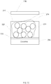
- FIG. 1 shows an example of a cross-sectional diagram of a substrate and a layer of antimony-doped tin oxide disposed on a surface of the substrate.
- LSPR Localized surface plasmon resonance
- Electrochemical doping of CdSe NC films was previously shown to bleach the exciton peak at the onset of the visible band gap absorption and to introduce a new intraband absorption peak in the far infrared region 11,12 .
- metal nanostructures e.g., Au or Ag
- acute screening by a high background charge density limits the shift of the LSPR peak to 10 or 20 nm, at most.
- Hydrocarbon ligands which cap the surfaces of NCs form highly insulating barriers between adjacent NCs. Simple air annealing causes the LSPR feature to disappear, consistent with the trapping of free carriers by filling structural oxygen vacancies 16 .
- the electrochromic device includes (1) a substrate and (2) a film supported by the substrate, where the film includes transparent conducting oxide (TCO) nanostructures.
- the electrochromic device further includes (a) an electrolyte, where the nanostructures are embedded in the electrolyte, resulting in an electrolyte, nanostructure mixture positioned above the substrate and (b) a counter electrode positioned above the mixture.
- the electrochromic device further includes a conductive coating deposited on the substrate between the substrate and the mixture.
- the electrochromic device further includes a second substrate positioned above the mixture.
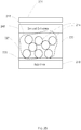
- an example includes a substrate 210 and a film 212 supported by substrate 210, where film 212 includes transparent conducting oxide (TCO) nanostructures 214.
- the device further includes an electrolyte 220, where nanostructures 214 are embedded in electrolyte 220, resulting in an electrolyte, nanostructure mixture 222 positioned above substrate 210 and a counter electrode 226 positioned above mixture 222.
- the embodiment further includes a conductive coating 230 deposited on substrate 210 between substrate 210 and mixture 222.
- the embodiment further includes a second substrate 240 positioned above mixture 222.
- substrate 210 includes glass. In an exemplary embodiment, substrate 210 includes a transparent material. In an exemplary embodiment, substrate 210 includes plastic. In an exemplary embodiment, substrate 210 includes polyethylene terephthalate (PET).
- PET polyethylene terephthalate
- nanostructures 214 include TCO nanocrystals. In an exemplary embodiment, nanostructures 214 include TCO nanowires. In an exemplary embodiment, nanostructures 214 include TCO nanorods. In an exemplary embodiment, nanostructures 214 include TCO nanoporous material.
- nanostructures 214 include tin-doped indium oxide (ITO). In an exemplary embodiment, nanostructures 214 include aluminum-doped zinc oxide (AZO). In an exemplary embodiment, nanostructures 214 include gallium-doped zinc oxide. In an exemplary embodiment, nanostructures 214 include indium, gallium-doped zinc oxide. In an exemplary embodiment, nanostructures 214 include indium-doped zinc oxide.
- electrolyte 220 includes an inorganic material. In an exemplary embodiment, electrolyte 220 includes a polymer. In an exemplary embodiment, electrolyte 220 includes a gel. In an exemplary embodiment, electrolyte 220 includes an organic liquid. In an exemplary embodiment, electrolyte 220 includes an aqueous liquid.
- counter electrode 226 includes an electrochromic film.
- counter electrode 226 includes a transition metal oxide.
- the transition metal oxide includes nickel oxide.
- the transition metal oxide includes vanadium oxide.
- the transition metal oxide includes comprises titanium oxide,
- conductive coating 230 includes a transparent material. In an exemplary embodiment, conductive coating 230 includes TCO. In an exemplary embodiment, conductive coating 230 includes graphene. In an exemplary embodiment, conductive coating 230 includes carbon nanorods. In an exemplary embodiment, conductive coating 230 includes metal nanowires.
- the embodiment includes synthesizing colloidal ITO NCs of variable size and doping level by balancing precursor reactivity and adjusting the indium and tin content in the feedstock, as shown in FIG. 3A, FIG. 3B, FIG. 3C, and FIG. 3D .
- Embodiments described herein include modifications of literature procedures 6,7 .
- the resulting NCs are capped with organic ligands that facilitate dispersion in hydrophobic solvents. Transmission spectra of these dispersions reveal well-defined LSPR peaks whose position relates to the doping level, as shown in FIG. 3E .
- the frequency of the LSPR ( ⁇ LSP ) is proportional to the bulk plasmon frequency ( ⁇ P ), which varies as square root of the free carrier concentration ( n )( 1 ).
- ⁇ LSP ⁇ ⁇ P ne 2 m * ⁇ 0
- the herein described embodiments' synthetic variation of the tin content manipulates n , which in turn adjusts ⁇ LSP .
- the LSPR resonance frequency varies much less strongly with size( 1 ), which is therefore available as a pseudo-independent variable in tuning the properties of our active coatings.
- the NCs were processed into electrically conducting films, approximately 150 nm thick, as shown in FIG. 4A .
- Deposition of uniform, non-scattering films by spin coating from a mixture of hexane and octane was facilitated by the hydrocarbon ligands which cap the surfaces of the NCs.
- these ligands form highly insulating barriers between adjacent NCs and had to be eliminated.
- Embodiments described herein include displacing the original, bulky oleic acid ligands with small molecules by submerging the NC film in a solution of formic acid, resulting in mass-action driven ligand exchange within the film 17 .
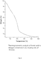
- Formic acid is volatile and can be desorbed by low temperature annealing in an inert environment, as shown in FIG. 5 .
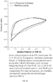
- the sheet resistance of the film drops with annealing temperature up to 500°C, but it is already sufficiently low following a 200°C anneal to conduct in-plane over centimeter-scale sample dimensions, as shown in FIG. 6 .
- Embodiments described herein include annealing the films at 250°C, which reproducibly gave well-conducting films with a low thermal budget.
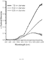
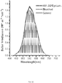
- the absorption peak shifted to longer wavelength, as shown in FIG. 4B , raising questions about possible changes in the free carrier concentration and the structure of the NC films.
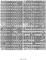
- the crystallite size remained fixed; the x-ray diffraction pattern and peak widths remained unchanged following annealing.
- An extended Drude model was employed to fit the optical transmission spectra. The model considered possible changes in the carrier concentration, the dielectric environment, the volume fraction of the NCs, as well as variations in damping that might arise as the NC surfaces are chemically modified 18,19 .
- the NC films were positioned as the working electrode in an electrochemical cell and in situ transmission spectra recorded as a function of the applied potential. Due to the onset of strong absorption bands of the electrolyte, the in situ measurements were limited to a spectral window of 400-2200 nm.
- the optical spectrum of the film at its open circuit voltage showed minimal change compared to its spectrum in an air environment, consistent with the change in dielectric environment and indicating that no chemical reactions occur at the NC surface.
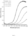
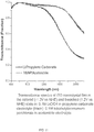
- the SPR peak shifted to higher energy and became more intense, as shown in FIG. 7A . Both changes were consistent with the modulation of the free carrier concentration, n , which would shift the plasmon resonance frequency, as in equation (1), and increase the extinction at the LSPR peak proportionally 1 .
- the modulation of the surface plasmon resonance in embodiments described herein is more analogous to that found in metallic nanostructures 34 and is related to that demonstrated recently at the planar interface of ITO with a dielectric layer 24 .
- the free carrier concentration in a thin ( ⁇ 5 nm) accumulation region was modulated by applying a potential between the ITO film and a counter electrode on the opposite side of the dielectric layer. Since plasmon resonance shifts to both shorter and longer wavelength than the initial state were observed, it is suggested that accumulation and depletion regions, respectively, are formed near the surface of the NCs. This hypothesis predicts greater modulation for smaller NCs, whose entire volume can lie within the strongly modulated accumulation/depletion region.
- the embodiments described herein can strongly modulate the plasmon frequency, and the associated free carrier concentration, throughout the volume of each NC and of the overall film to account for the nearly constant ⁇ LSP even as electrons were injected or extracted.
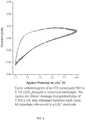
- a principle degradation pathway for battery and electrochromic electrode materials namely strain from repeated intercalation and deintercalation 26 , was thus circumvented by the capacitive operating mechanism of the embodiments described herein.
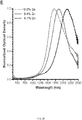
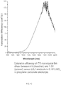
- the coloration efficiency is also improved by several fold over conventional electrochromic films, as shown in FIG. 12 .
- the efficacy of compensating injected carriers capacitively, without intercalation is not limited to the choice of ITO as an electrode material; it is rather a direct consequence of nanostructuring on the single-digit nanometer scale. Any material which undergoes a change in optical properties upon charging and discharging, including other plasmonic NCs, but also conventional electrochromic materials like WO 3 , could, in principle, be operated in this manner 27 , Hence, the embodiments described herein suggest a new paradigm for the design of nanocrystal-based electrochromic electrodes that are robust to cycling, greatly expanding options for material selection to achieve targeted optical response characteristics for smart windows and other applications of optical modulation.
- the electrochemical modulation of transmittance through the embodiments described herein is of particular interest for dynamic "smart window" applications.
- the embodiments described herein could be effectively part of a macroplasmonic device, operating on nanoplasmonic principles.
- the heat load derived from solar infrared radiation could be dynamically modulated in response to the changing outdoor environment by the embodiments described herein, while visible light transmittance could be maintained for daylighting use 25 by the embodiments described herein.
- the embodiments described herein demonstrate that the surface plasmon resonance of ITO NC films can be dynamically tuned through fully reversible electrochemical doping, hence realizing the promise of electrical manipulation of semiconductor LSPR features.
- the LSPR modulation of the embodiments described herein is a collective response of the free electrons, more analogous to the electrochemical response of Au or Ag LSPR 13,14 .
- LSPR of the embodiments described herein can shift dynamically across a range covering much of the near infrared (NIR) spectrum (including telecommunications wavelengths), opening the door to potential applications including controlling optical coupling into or out of nanoplasmonic devices or tuning plasmonic enhancement of spectroscopic signatures 15 .
- NIR near infrared
- the embodiments described herein could dynamically modulate transmittance of solar infrared radiation. Considering their excellent visible transparency, such modulation offers a unique opportunity for a dynamic coating on advanced, energy-saving "smart windows.”
- Indium acetylacetonate (In(acac)3, 99.99%), tin bis(acetylacetonate) dichloride (Sn(acac)2Cl2, 98 %), tin acetate (Sn(Ac)4 99.99%), myristic acid (MA, ⁇ 98%), 1-octadecene (ODE, 90%), and oleic acid (OLAC, 90%) were purchased from Aldrich and used without further purification. Oleylamine (OLAM, 90%) was obtained from Acros.
- NCs ITO nanocrystals
- Elemental analysis was performed by induced coupled plasma atomic emission spectroscopy (ICP-AES) with a Varian 720/730 Series spectrometer.
- the ITO samples were digested in concentrated HCl.
- the relative error on the extracted Sn content was within 3% of the reported percentage, as evaluated on the basis of 9 replicates per each measurement.
- a spincasting technique was used to generate thin films of ITO nanocrystals. Glass substrates were cleaned via sonication in a three step process: 15 min de-ionized water with 2% Helmenex solution, 15 min acetone, 15 min isopropanol. Three rinses were performed between each sonication step. Using a one to one octane/hexane solution of ITO nanocrystals ( ⁇ 67 mg/ml), 30ul where dispensed on a 2.5cm x 2.5cm glass substrate. Spinning recipe consist of an initial 1000RPM spin for 30 seconds followed by a 4000RPM spin for 20 seconds.
- Film thickness was measured between each post processing step using a Vecco Dektak 150+ Profiler and confirmed with 90 degree cross section images using a Zeiss Gemini Ultra-55 Analytical Scanning Electron Microscope. Film morphology was checked between post processing step using a Bruker D8-Discover X-ray diffractometer equipped with a GADDS area detector and operated at 40 kV and 20 mA at the wavelength of Cu K ⁇ , 1.54 A.
- a Ag/Ag + reference electrode consisting of a silver wire immersed in a 0.01M AgNO3/0.1M THAP/acetonitrile solution was used as a reference electrode.
- the films were driven between a potential range of -1.55V and 0.95V versus the reference electrode in order to match the conditions set by the lithium based electrolyte. Coloration efficiency was calculated by taking the ratio of the change in optical density between the positive and negative bias with its associated charge per unit area. All electrochemical measurements were performed in an argon glove box with a Bio-logic VSP potentiostat and a ASD Quality Spec Pro VIS/NIR spectrometer.
- the Maxwell-Garnett (MG) effective medium approximation was used to model the ITO nanocrystal layers.
- Bruggeman effective medium approximation is used for conductive nanocrystal films when the volume fractions are above about 0.3(18,19).
- this model did not provide as good of a fit for the thin films in this study, which had volume fractions of 0.4 and higher. This was surprising since Bruggeman's model accounts for electronic coupling between particles and the ITO films were all laterally conductive when tested with 4 point probe measurements.
- the fourth and final component was the free carrier absorption described by the extended Drude theory.
- Ionized impurity scattering is known to play an important role in the electronic transport in highly doped semiconductors. Such scattering is accounted for in the extended Drude theory by taking into account the frequency dependence of the damping constant.
- a commonly used empirical model was chosen which has proven useful for ITO(19,29). It gives very similar results as other analytical models(18,30) which account for the ⁇ -3/2 dependence(31) of the damping parameter.
Landscapes
- Physics & Mathematics (AREA)
- Nonlinear Science (AREA)
- Engineering & Computer Science (AREA)
- Optics & Photonics (AREA)
- Chemical & Material Sciences (AREA)
- Nanotechnology (AREA)
- General Physics & Mathematics (AREA)
- Structural Engineering (AREA)
- Life Sciences & Earth Sciences (AREA)
- Biophysics (AREA)
- Crystallography & Structural Chemistry (AREA)
- Architecture (AREA)
- Civil Engineering (AREA)
- Inorganic Chemistry (AREA)
- Electrochromic Elements, Electrophoresis, Or Variable Reflection Or Absorption Elements (AREA)
Claims (11)
- Dispositif électrochromique, comprenant :un substrat (210) ;un film électrochromique (212) positionné sur le substrat (210) et comprenant un mélange électrolyte-nanostructures formé de nanostructures (214) d'oxyde conducteur transparent, TCO, noyées dans un électrolyte (220) etune contre-électrode (226) positionnée au-dessus du film électrochromique (212),dans lequel un pic d'absorbance du film électrochromique (212) se trouve à une première longueur d'onde dans une plage de longueurs d'onde infrarouge à une tension de circuit ouvert,caractérisé en ce quele film électrochromique (212) est configuré de sorte que le pic d'absorbance se déplace vers une seconde longueur d'onde dans la plage infrarouge qui est différente de la première longueur d'onde en réponse à une tension de polarisation appliquée qui est différente de la tension de circuit ouvert, la tension de polarisation appliquée créant des régions d'accumulation et de déplétion à proximité de la surface des nanostructures de TCO (214), etdans lequel le pic d'absorbance du film se décale vers la seconde longueur d'onde en raison d'un déplacement correspondant d'un pic de résonance plasmonique de surface des nanostructures de TCO (214) en réponse à la tension de polarisation appliquée.
- Fenêtre intelligente comprenant le dispositif selon la revendication 1.
- Dispositif selon la revendication 1, dans lequel les nanostructures de TCO sont choisies dans le groupe de l'oxyde d'indium dopé à l'étain, ITO, de l'oxyde de zinc dopé à l'aluminium, AZO, de l'oxyde de zinc dopé au gallium, de l'oxyde de zinc dopé à l'indium, et de l'oxyde de zinc dopé à l'indium et au gallium.
- Dispositif selon la revendication 1, dans lequel l'électrolyte comprend un polymère.
- Dispositif selon la revendication 1, dans lequel l'électrolyte comprend un gel.
- Procédé de fonctionnement d'un dispositif électrochromique, comprenant :se procurer le dispositif électrochromique comprenant un substrat (210), une contre-électrode (226), et un film électrochromique (212) qui comprend un mélange formé de nanostructures (214) d'oxyde conducteur transparent, TCO, noyées dans un électrolyte (220), et disposé entre le substrat et la contre-électrode (226), le film électrochromique (212) étant positionné sur le substrat (210),dans lequel un pic d'absorbance du film électrochromique (212) se trouve à une première longueur d'onde dans une plage de longueurs d'onde infrarouge à une tension de circuit ouvert ; etappliquer une tension de polarisation au dispositif pour déplacer le pic d'absorbance infrarouge du film électrochromique (212) vers une seconde longueur d'onde dans la plage de longueurs d'onde infrarouge différente de la première longueur d'onde, en raison d'un déplacement correspondant d'un pic de résonance plasmonique de surface des nanostructures de TCO (214) en réponse à l'application de la tension de polarisation,dans lequel la tension de polarisation est différente de la tension de circuit ouvert et crée une accumulation et une déplétion de porteurs de charge à proximité de la surface des nanostructures de TCO (214).
- Procédé selon la revendication 6, dans lequel le dispositif est une fenêtre intelligente.
- Procédé selon la revendication 6, dans lequel les nanostructures de TCO sont choisies dans le groupe de l'oxyde d'indium dopé à l'étain ITO, de l'oxyde de zinc dopé à l'aluminium AZO, de l'oxyde de zinc dopé au gallium, de l'oxyde de zinc dopé à l'indium, et de l'oxyde de zinc dopé à l'indium et au gallium.
- Procédé selon la revendication 6, dans lequel, en outre, la contre-électrode et un second substrat sont positionnés au-dessus du film électrochromique.
- Procédé selon la revendication 6, dans lequel l'électrolyte comprend un polymère.
- Procédé selon la revendication 6, dans lequel l'électrolyte comprend un gel.
Applications Claiming Priority (2)
| Application Number | Priority Date | Filing Date | Title |
|---|---|---|---|
| US201161528124P | 2011-08-26 | 2011-08-26 | |
| PCT/US2012/051757 WO2013032790A2 (fr) | 2011-08-26 | 2012-08-21 | Dispositif électrochromique à oxyde conducteur transparent nanostructuré |
Publications (3)
| Publication Number | Publication Date |
|---|---|
| EP2748867A2 EP2748867A2 (fr) | 2014-07-02 |
| EP2748867A4 EP2748867A4 (fr) | 2015-04-01 |
| EP2748867B1 true EP2748867B1 (fr) | 2019-03-13 |
Family
ID=47757122
Family Applications (1)
| Application Number | Title | Priority Date | Filing Date |
|---|---|---|---|
| EP12828240.7A Active EP2748867B1 (fr) | 2011-08-26 | 2012-08-21 | Dispositif électrochromique à oxyde conducteur transparent nanostructuré |
Country Status (6)
| Country | Link |
|---|---|
| US (1) | US9341913B2 (fr) |
| EP (1) | EP2748867B1 (fr) |
| JP (1) | JP2014525607A (fr) |
| KR (1) | KR101953180B1 (fr) |
| CN (1) | CN103858242B (fr) |
| WO (1) | WO2013032790A2 (fr) |
Families Citing this family (26)
| Publication number | Priority date | Publication date | Assignee | Title |
|---|---|---|---|---|
| US9595363B2 (en) * | 2012-12-06 | 2017-03-14 | The Regents Of The University Of California | Surface chemical modification of nanocrystals |
| CN103144380B (zh) * | 2013-03-22 | 2016-08-03 | 中国南玻集团股份有限公司 | 三银调光玻璃 |
| CN104142584B (zh) * | 2013-07-16 | 2017-02-01 | 中国科学院广州能源研究所 | 一种氧化物纳米线型电光薄膜的制备方法 |
| KR101544489B1 (ko) | 2014-02-06 | 2015-08-13 | 인하대학교 산학협력단 | 겔 전해질에서 구동하는 전기변색 소자 및 이의 제조방법 |
| US10585322B2 (en) | 2014-04-15 | 2020-03-10 | The Regents Of The University Of California | Methods for producing electrochromic films by low temperature condensation of polyoxometalates |
| US9798214B2 (en) * | 2015-02-19 | 2017-10-24 | Heliotrope Technologies Inc. | Methods of charging solid state plasmonic electrochromic smart window devices |
| CN105119158A (zh) * | 2015-09-28 | 2015-12-02 | 吴本刚 | 具有电致变色器件外箱的变电柜及其制作方法 |
| WO2017106160A1 (fr) * | 2015-12-15 | 2017-06-22 | Board Of Regents, The University Of Texas System | Films conducteurs nanostructurés avec répartition hétérogène de dopant et procédés pour leur fabrication et leur utilisation |
| JP6665210B2 (ja) * | 2016-02-15 | 2020-03-13 | シャープ株式会社 | エレクトロクロミックデバイス、およびエレクトロクロミックデバイスを備えるスマートウインドウ |
| KR101945434B1 (ko) * | 2016-04-25 | 2019-02-08 | 한국에너지기술연구원 | 리간드-금속산화물층을 포함하는 자기구동 전기변색소자 |
| KR101862200B1 (ko) * | 2016-09-06 | 2018-07-06 | 주식회사 석원 | 전기변색 기판 시스템, 전기변색 기판 시스템이 이용되는 스마트 윈도우 기판 시스템 및 스마트 윈도우 기판 시스템의 제작 방법 |
| JP6794727B2 (ja) * | 2016-09-06 | 2020-12-02 | コニカミノルタ株式会社 | 構造色変化型材料及び歪み検出装置 |
| US10944398B2 (en) | 2016-09-30 | 2021-03-09 | Uchicago Argonne, Llc | Systems and methods for ultrafast plasmonic response in doped, colloidal nanostructures |
| CN106896260A (zh) * | 2017-02-09 | 2017-06-27 | 广东电网有限责任公司云浮供电局 | 一种验电涂层及验电方法 |
| CN107450223B (zh) * | 2017-08-18 | 2020-11-03 | 京东方科技集团股份有限公司 | 变色单元、显示模组及其制作方法和显示控制方法 |
| CN109822996A (zh) * | 2017-11-23 | 2019-05-31 | 宸美(厦门)光电有限公司 | 电控变色车用玻璃 |
| WO2019172133A1 (fr) * | 2018-03-05 | 2019-09-12 | シャープ株式会社 | Élément électrochromique et fenêtre intelligente |
| US10775649B2 (en) | 2018-05-17 | 2020-09-15 | Cardinal Cg Company | Elastomeric optical device and related methods |
| US11340479B2 (en) | 2018-05-17 | 2022-05-24 | Cardinal Cg Company | Elastomeric optical device and related operation methods |
| CN109207171B (zh) * | 2018-08-24 | 2022-02-01 | 华南师范大学 | 一种液晶器件及金属氧化物纳米颗粒在液晶器件中的应用 |
| KR102052440B1 (ko) * | 2018-08-29 | 2019-12-05 | 서울시립대학교 산학협력단 | 전기 변색성 슈퍼 커패시터 |
| CN109298481B (zh) * | 2018-10-09 | 2019-09-10 | 东北大学 | 自发产生spr效应的金属银填充光子晶体光纤及其制法 |
| WO2020107126A1 (fr) | 2018-11-30 | 2020-06-04 | Ma Joseph J K | Dispositifs, systèmes et procédés optiques électrochromatiques |
| CN109945996A (zh) * | 2019-03-21 | 2019-06-28 | 苏州大学 | 一种新型机器人电子皮肤及其制备方法 |
| US12578608B2 (en) | 2020-08-11 | 2026-03-17 | Council Of Scientific & Industrial Research | Electrochromic bi-layered devices for dynamic light throughput control and a process for the preparation thereof |
| JPWO2022190690A1 (fr) * | 2021-03-10 | 2022-09-15 |
Family Cites Families (23)
| Publication number | Priority date | Publication date | Assignee | Title |
|---|---|---|---|---|
| US4573768A (en) * | 1983-12-05 | 1986-03-04 | The Signal Companies, Inc. | Electrochromic devices |
| FR2690536B1 (fr) * | 1992-04-28 | 1994-06-17 | Saint Gobain Vitrage Int | Vitrage electrochrome. |
| DE69830566T2 (de) * | 1997-02-06 | 2006-05-11 | University College Dublin | Elektrochromes system |
| US5995273A (en) | 1998-02-25 | 1999-11-30 | Ashwin-Ushas Corporation | Electrochromic display device |
| DE19914093A1 (de) | 1999-03-27 | 2000-10-19 | Dornier Gmbh | Elektrochromes Element |
| WO2005062110A1 (fr) * | 2003-12-22 | 2005-07-07 | Lg Chem, Ltd. | Matiere electrochromique a duree de vie prolongee |
| KR20080044233A (ko) * | 2005-08-22 | 2008-05-20 | 코나르카 테크놀로지, 인코포레이티드 | 일체형 광전지를 갖는 디스플레이 |
| KR100732849B1 (ko) | 2005-12-21 | 2007-06-27 | 삼성에스디아이 주식회사 | 유기 발광 표시장치 |
| US7403319B2 (en) | 2006-01-13 | 2008-07-22 | Ntera Limited | Electrochromic device employing gel or solid polymers having specific channel direction for the conduction of ions |
| DE102006017356B4 (de) | 2006-04-11 | 2015-12-17 | Flabeg Deutschland Gmbh | Verfahren zur Herstellung eines Mehrschichtsystems auf einem Träger, insbesondere in einem elektrochromen Element |
| TW200834610A (en) | 2007-01-10 | 2008-08-16 | Nitto Denko Corp | Transparent conductive film and method for producing the same |
| CN103777417B (zh) * | 2007-04-20 | 2017-01-18 | 凯姆控股有限公司 | 复合透明导体及其形成方法 |
| KR100865629B1 (ko) | 2007-06-05 | 2008-10-27 | 삼성전자주식회사 | 표시 특성이 향상된 전기변색 소자 및 그 제조 방법 |
| US8593714B2 (en) * | 2008-05-19 | 2013-11-26 | Ajjer, Llc | Composite electrode and electrolytes comprising nanoparticles and resulting devices |
| KR101435196B1 (ko) | 2007-10-11 | 2014-08-28 | 삼성전자주식회사 | 폴리프탈레이트계 고분자를 이용한 전기변색 소자 및 그제조방법 |
| JP2009175718A (ja) | 2007-12-28 | 2009-08-06 | Fujifilm Corp | エレクトロデポジション方式の調光デバイス、及びエレクトロデポジション方式の反射型表示装置 |
| JP5453725B2 (ja) * | 2008-03-11 | 2014-03-26 | 株式会社リコー | エレクトロクロミック化合物およびそれを用いたエレクトロクロミック表示素子 |
| WO2009143625A1 (fr) * | 2008-05-30 | 2009-12-03 | Opalux Incorporated | Empilement de bragg accordable |
| JP5337519B2 (ja) * | 2009-02-10 | 2013-11-06 | 株式会社東芝 | 表示装置及び表示方法 |
| US8858748B2 (en) * | 2009-08-27 | 2014-10-14 | Guardian Industries Corp. | Electrochromic devices, assemblies incorporating electrochromic devices, and/or methods of making the same |
| CN101833211B (zh) * | 2010-04-01 | 2011-11-02 | 中国科学院宁波材料技术与工程研究所 | 一种智能调光玻璃 |
| HK1201102A1 (en) | 2011-07-25 | 2015-08-21 | 加州大学校务委员会 | Electrochromic nanocomposite films |
| WO2013154779A1 (fr) * | 2012-04-10 | 2013-10-17 | The Regents Of The University Of California | Dispositif électrochimique nanocomposite nanocristallin-polymère |
-
2012
- 2012-08-21 EP EP12828240.7A patent/EP2748867B1/fr active Active
- 2012-08-21 US US14/240,689 patent/US9341913B2/en active Active
- 2012-08-21 WO PCT/US2012/051757 patent/WO2013032790A2/fr not_active Ceased
- 2012-08-21 KR KR1020147008063A patent/KR101953180B1/ko active Active
- 2012-08-21 JP JP2014528451A patent/JP2014525607A/ja active Pending
- 2012-08-21 CN CN201280041759.3A patent/CN103858242B/zh active Active
Non-Patent Citations (1)
| Title |
|---|
| None * |
Also Published As
| Publication number | Publication date |
|---|---|
| CN103858242A (zh) | 2014-06-11 |
| JP2014525607A (ja) | 2014-09-29 |
| CN103858242B (zh) | 2016-08-17 |
| WO2013032790A2 (fr) | 2013-03-07 |
| EP2748867A4 (fr) | 2015-04-01 |
| KR20140063741A (ko) | 2014-05-27 |
| KR101953180B1 (ko) | 2019-02-28 |
| WO2013032790A3 (fr) | 2014-05-08 |
| US9341913B2 (en) | 2016-05-17 |
| US20150109652A1 (en) | 2015-04-23 |
| EP2748867A2 (fr) | 2014-07-02 |
Similar Documents
| Publication | Publication Date | Title |
|---|---|---|
| EP2748867B1 (fr) | Dispositif électrochromique à oxyde conducteur transparent nanostructuré | |
| Garcia et al. | Dynamically modulating the surface plasmon resonance of doped semiconductor nanocrystals | |
| Arslan et al. | Fast electrochromic response and high coloration efficiency of Al-doped WO3 thin films for smart window applications | |
| Agrawal et al. | Control of localized surface plasmon resonances in metal oxide nanocrystals | |
| Runnerstrom et al. | Nanostructured electrochromic smart windows: traditional materials and NIR-selective plasmonic nanocrystals | |
| Naseri et al. | Improved electrochromical properties of sol–gel WO3 thin films by doping gold nanocrystals | |
| Tandon et al. | Competition between depletion effects and coupling in the plasmon modulation of doped metal oxide nanocrystals | |
| Santhosh et al. | Effect of ablation rate on the microstructure and electrochromic properties of pulsed-laser-deposited molybdenum oxide thin films | |
| Chen et al. | The birth of zinc anode-based electrochromic devices | |
| Acuña et al. | Sputtering power effects on the electrochromic properties of NiO films | |
| Giannuzzi et al. | Tunable near-infrared localized surface plasmon resonance of F, In-Codoped CdO nanocrystals | |
| Liu et al. | Plasmonic-based electrochromic materials and devices | |
| Jamdegni et al. | Electrochromic behavior of highly stable, flexible electrochromic electrode based on covalently bonded polyaniline-graphene quantum dot composite | |
| Asami et al. | Electrochemical redox-based tuning of near infrared localized plasmons of CuS nanoplates | |
| Pullar et al. | High colouring efficiency, optical density and inserted charge in sol–gel derived electrochromic titania nanostructures | |
| Yamazaki et al. | Determination of W (V) in WO3 photochromism using localized surface plasmon resonance of Ag nanoparticles | |
| Shubert-Zuleta et al. | How Depletion Layers Govern the Dynamic Plasmonic Response of In-doped CdO Nanocrystals | |
| Bhandari et al. | Charge transport and electrochromism in novel nanocomposite films of poly (3, 4-ethylenedioxythiophene)-Au nanoparticles− CdSe quantum dots | |
| Haritha et al. | Sol–gel derived ZnO thin film as a transparent counter electrode for WO3 based electrochromic devices | |
| Song et al. | Tunable optical constants of aluminum tungsten bronzes in electrochromic tungsten oxide thin films | |
| Vuk et al. | Structural and spectroelectrochemical (UV–vis and IR) studies of nanocrystalline sol–gel derived TiO2 films | |
| Kadam et al. | Enhanced optical modulation due to SPR in gold nanoparticles embedded WO3 thin films | |
| Zhang et al. | Preparation, characterization and electrochromic properties of amorphous Gd-doped TiO2 films | |
| Zhang et al. | Preparation, optimization and electrochromic properties of dual-band device with four modes | |
| Daniels et al. | Spectroelectrochemical studies of plasmon coupled silver nanoparticles |
Legal Events
| Date | Code | Title | Description |
|---|---|---|---|
| PUAI | Public reference made under article 153(3) epc to a published international application that has entered the european phase |
Free format text: ORIGINAL CODE: 0009012 |
|
| 17P | Request for examination filed |
Effective date: 20140228 |
|
| AK | Designated contracting states |
Kind code of ref document: A2 Designated state(s): AL AT BE BG CH CY CZ DE DK EE ES FI FR GB GR HR HU IE IS IT LI LT LU LV MC MK MT NL NO PL PT RO RS SE SI SK SM TR |
|
| A4 | Supplementary search report drawn up and despatched |
Effective date: 20150304 |
|
| RIC1 | Information provided on ipc code assigned before grant |
Ipc: B82Y 20/00 20110101ALI20150226BHEP Ipc: G02F 1/155 20060101AFI20150226BHEP |
|
| DAX | Request for extension of the european patent (deleted) | ||
| STAA | Information on the status of an ep patent application or granted ep patent |
Free format text: STATUS: EXAMINATION IS IN PROGRESS |
|
| 17Q | First examination report despatched |
Effective date: 20170207 |
|
| GRAP | Despatch of communication of intention to grant a patent |
Free format text: ORIGINAL CODE: EPIDOSNIGR1 |
|
| STAA | Information on the status of an ep patent application or granted ep patent |
Free format text: STATUS: GRANT OF PATENT IS INTENDED |
|
| INTG | Intention to grant announced |
Effective date: 20180810 |
|
| GRAS | Grant fee paid |
Free format text: ORIGINAL CODE: EPIDOSNIGR3 |
|
| GRAJ | Information related to disapproval of communication of intention to grant by the applicant or resumption of examination proceedings by the epo deleted |
Free format text: ORIGINAL CODE: EPIDOSDIGR1 |
|
| GRAL | Information related to payment of fee for publishing/printing deleted |
Free format text: ORIGINAL CODE: EPIDOSDIGR3 |
|
| STAA | Information on the status of an ep patent application or granted ep patent |
Free format text: STATUS: EXAMINATION IS IN PROGRESS |
|
| GRAR | Information related to intention to grant a patent recorded |
Free format text: ORIGINAL CODE: EPIDOSNIGR71 |
|
| STAA | Information on the status of an ep patent application or granted ep patent |
Free format text: STATUS: GRANT OF PATENT IS INTENDED |
|
| GRAA | (expected) grant |
Free format text: ORIGINAL CODE: 0009210 |
|
| STAA | Information on the status of an ep patent application or granted ep patent |
Free format text: STATUS: THE PATENT HAS BEEN GRANTED |
|
| INTC | Intention to grant announced (deleted) | ||
| INTG | Intention to grant announced |
Effective date: 20190128 |
|
| AK | Designated contracting states |
Kind code of ref document: B1 Designated state(s): AL AT BE BG CH CY CZ DE DK EE ES FI FR GB GR HR HU IE IS IT LI LT LU LV MC MK MT NL NO PL PT RO RS SE SI SK SM TR |
|
| REG | Reference to a national code |
Ref country code: GB Ref legal event code: FG4D |
|
| REG | Reference to a national code |
Ref country code: CH Ref legal event code: EP Ref country code: AT Ref legal event code: REF Ref document number: 1108507 Country of ref document: AT Kind code of ref document: T Effective date: 20190315 |
|
| REG | Reference to a national code |
Ref country code: IE Ref legal event code: FG4D |
|
| REG | Reference to a national code |
Ref country code: DE Ref legal event code: R096 Ref document number: 602012057851 Country of ref document: DE |
|
| REG | Reference to a national code |
Ref country code: NL Ref legal event code: MP Effective date: 20190313 |
|
| REG | Reference to a national code |
Ref country code: LT Ref legal event code: MG4D |
|
| PG25 | Lapsed in a contracting state [announced via postgrant information from national office to epo] |
Ref country code: NO Free format text: LAPSE BECAUSE OF FAILURE TO SUBMIT A TRANSLATION OF THE DESCRIPTION OR TO PAY THE FEE WITHIN THE PRESCRIBED TIME-LIMIT Effective date: 20190613 Ref country code: SE Free format text: LAPSE BECAUSE OF FAILURE TO SUBMIT A TRANSLATION OF THE DESCRIPTION OR TO PAY THE FEE WITHIN THE PRESCRIBED TIME-LIMIT Effective date: 20190313 Ref country code: FI Free format text: LAPSE BECAUSE OF FAILURE TO SUBMIT A TRANSLATION OF THE DESCRIPTION OR TO PAY THE FEE WITHIN THE PRESCRIBED TIME-LIMIT Effective date: 20190313 Ref country code: LT Free format text: LAPSE BECAUSE OF FAILURE TO SUBMIT A TRANSLATION OF THE DESCRIPTION OR TO PAY THE FEE WITHIN THE PRESCRIBED TIME-LIMIT Effective date: 20190313 |
|
| PG25 | Lapsed in a contracting state [announced via postgrant information from national office to epo] |
Ref country code: LV Free format text: LAPSE BECAUSE OF FAILURE TO SUBMIT A TRANSLATION OF THE DESCRIPTION OR TO PAY THE FEE WITHIN THE PRESCRIBED TIME-LIMIT Effective date: 20190313 Ref country code: NL Free format text: LAPSE BECAUSE OF FAILURE TO SUBMIT A TRANSLATION OF THE DESCRIPTION OR TO PAY THE FEE WITHIN THE PRESCRIBED TIME-LIMIT Effective date: 20190313 Ref country code: HR Free format text: LAPSE BECAUSE OF FAILURE TO SUBMIT A TRANSLATION OF THE DESCRIPTION OR TO PAY THE FEE WITHIN THE PRESCRIBED TIME-LIMIT Effective date: 20190313 Ref country code: GR Free format text: LAPSE BECAUSE OF FAILURE TO SUBMIT A TRANSLATION OF THE DESCRIPTION OR TO PAY THE FEE WITHIN THE PRESCRIBED TIME-LIMIT Effective date: 20190614 Ref country code: RS Free format text: LAPSE BECAUSE OF FAILURE TO SUBMIT A TRANSLATION OF THE DESCRIPTION OR TO PAY THE FEE WITHIN THE PRESCRIBED TIME-LIMIT Effective date: 20190313 Ref country code: BG Free format text: LAPSE BECAUSE OF FAILURE TO SUBMIT A TRANSLATION OF THE DESCRIPTION OR TO PAY THE FEE WITHIN THE PRESCRIBED TIME-LIMIT Effective date: 20190613 |
|
| REG | Reference to a national code |
Ref country code: AT Ref legal event code: MK05 Ref document number: 1108507 Country of ref document: AT Kind code of ref document: T Effective date: 20190313 |
|
| PG25 | Lapsed in a contracting state [announced via postgrant information from national office to epo] |
Ref country code: ES Free format text: LAPSE BECAUSE OF FAILURE TO SUBMIT A TRANSLATION OF THE DESCRIPTION OR TO PAY THE FEE WITHIN THE PRESCRIBED TIME-LIMIT Effective date: 20190313 Ref country code: EE Free format text: LAPSE BECAUSE OF FAILURE TO SUBMIT A TRANSLATION OF THE DESCRIPTION OR TO PAY THE FEE WITHIN THE PRESCRIBED TIME-LIMIT Effective date: 20190313 Ref country code: CZ Free format text: LAPSE BECAUSE OF FAILURE TO SUBMIT A TRANSLATION OF THE DESCRIPTION OR TO PAY THE FEE WITHIN THE PRESCRIBED TIME-LIMIT Effective date: 20190313 Ref country code: SK Free format text: LAPSE BECAUSE OF FAILURE TO SUBMIT A TRANSLATION OF THE DESCRIPTION OR TO PAY THE FEE WITHIN THE PRESCRIBED TIME-LIMIT Effective date: 20190313 Ref country code: RO Free format text: LAPSE BECAUSE OF FAILURE TO SUBMIT A TRANSLATION OF THE DESCRIPTION OR TO PAY THE FEE WITHIN THE PRESCRIBED TIME-LIMIT Effective date: 20190313 Ref country code: IT Free format text: LAPSE BECAUSE OF FAILURE TO SUBMIT A TRANSLATION OF THE DESCRIPTION OR TO PAY THE FEE WITHIN THE PRESCRIBED TIME-LIMIT Effective date: 20190313 Ref country code: AL Free format text: LAPSE BECAUSE OF FAILURE TO SUBMIT A TRANSLATION OF THE DESCRIPTION OR TO PAY THE FEE WITHIN THE PRESCRIBED TIME-LIMIT Effective date: 20190313 Ref country code: PT Free format text: LAPSE BECAUSE OF FAILURE TO SUBMIT A TRANSLATION OF THE DESCRIPTION OR TO PAY THE FEE WITHIN THE PRESCRIBED TIME-LIMIT Effective date: 20190713 |
|
| PG25 | Lapsed in a contracting state [announced via postgrant information from national office to epo] |
Ref country code: SM Free format text: LAPSE BECAUSE OF FAILURE TO SUBMIT A TRANSLATION OF THE DESCRIPTION OR TO PAY THE FEE WITHIN THE PRESCRIBED TIME-LIMIT Effective date: 20190313 Ref country code: PL Free format text: LAPSE BECAUSE OF FAILURE TO SUBMIT A TRANSLATION OF THE DESCRIPTION OR TO PAY THE FEE WITHIN THE PRESCRIBED TIME-LIMIT Effective date: 20190313 |
|
| REG | Reference to a national code |
Ref country code: DE Ref legal event code: R097 Ref document number: 602012057851 Country of ref document: DE |
|
| PG25 | Lapsed in a contracting state [announced via postgrant information from national office to epo] |
Ref country code: AT Free format text: LAPSE BECAUSE OF FAILURE TO SUBMIT A TRANSLATION OF THE DESCRIPTION OR TO PAY THE FEE WITHIN THE PRESCRIBED TIME-LIMIT Effective date: 20190313 Ref country code: IS Free format text: LAPSE BECAUSE OF FAILURE TO SUBMIT A TRANSLATION OF THE DESCRIPTION OR TO PAY THE FEE WITHIN THE PRESCRIBED TIME-LIMIT Effective date: 20190713 |
|
| PLBE | No opposition filed within time limit |
Free format text: ORIGINAL CODE: 0009261 |
|
| STAA | Information on the status of an ep patent application or granted ep patent |
Free format text: STATUS: NO OPPOSITION FILED WITHIN TIME LIMIT |
|
| PG25 | Lapsed in a contracting state [announced via postgrant information from national office to epo] |
Ref country code: DK Free format text: LAPSE BECAUSE OF FAILURE TO SUBMIT A TRANSLATION OF THE DESCRIPTION OR TO PAY THE FEE WITHIN THE PRESCRIBED TIME-LIMIT Effective date: 20190313 |
|
| 26N | No opposition filed |
Effective date: 20191216 |
|
| PG25 | Lapsed in a contracting state [announced via postgrant information from national office to epo] |
Ref country code: SI Free format text: LAPSE BECAUSE OF FAILURE TO SUBMIT A TRANSLATION OF THE DESCRIPTION OR TO PAY THE FEE WITHIN THE PRESCRIBED TIME-LIMIT Effective date: 20190313 |
|
| PG25 | Lapsed in a contracting state [announced via postgrant information from national office to epo] |
Ref country code: TR Free format text: LAPSE BECAUSE OF FAILURE TO SUBMIT A TRANSLATION OF THE DESCRIPTION OR TO PAY THE FEE WITHIN THE PRESCRIBED TIME-LIMIT Effective date: 20190313 |
|
| PG25 | Lapsed in a contracting state [announced via postgrant information from national office to epo] |
Ref country code: LI Free format text: LAPSE BECAUSE OF NON-PAYMENT OF DUE FEES Effective date: 20190831 Ref country code: CH Free format text: LAPSE BECAUSE OF NON-PAYMENT OF DUE FEES Effective date: 20190831 Ref country code: MC Free format text: LAPSE BECAUSE OF FAILURE TO SUBMIT A TRANSLATION OF THE DESCRIPTION OR TO PAY THE FEE WITHIN THE PRESCRIBED TIME-LIMIT Effective date: 20190313 Ref country code: LU Free format text: LAPSE BECAUSE OF NON-PAYMENT OF DUE FEES Effective date: 20190821 |
|
| REG | Reference to a national code |
Ref country code: BE Ref legal event code: MM Effective date: 20190831 |
|
| PG25 | Lapsed in a contracting state [announced via postgrant information from national office to epo] |
Ref country code: IE Free format text: LAPSE BECAUSE OF NON-PAYMENT OF DUE FEES Effective date: 20190821 |
|
| PG25 | Lapsed in a contracting state [announced via postgrant information from national office to epo] |
Ref country code: BE Free format text: LAPSE BECAUSE OF NON-PAYMENT OF DUE FEES Effective date: 20190831 |
|
| PG25 | Lapsed in a contracting state [announced via postgrant information from national office to epo] |
Ref country code: CY Free format text: LAPSE BECAUSE OF FAILURE TO SUBMIT A TRANSLATION OF THE DESCRIPTION OR TO PAY THE FEE WITHIN THE PRESCRIBED TIME-LIMIT Effective date: 20190313 |
|
| PG25 | Lapsed in a contracting state [announced via postgrant information from national office to epo] |
Ref country code: HU Free format text: LAPSE BECAUSE OF FAILURE TO SUBMIT A TRANSLATION OF THE DESCRIPTION OR TO PAY THE FEE WITHIN THE PRESCRIBED TIME-LIMIT; INVALID AB INITIO Effective date: 20120821 Ref country code: MT Free format text: LAPSE BECAUSE OF FAILURE TO SUBMIT A TRANSLATION OF THE DESCRIPTION OR TO PAY THE FEE WITHIN THE PRESCRIBED TIME-LIMIT Effective date: 20190313 |
|
| PG25 | Lapsed in a contracting state [announced via postgrant information from national office to epo] |
Ref country code: MK Free format text: LAPSE BECAUSE OF FAILURE TO SUBMIT A TRANSLATION OF THE DESCRIPTION OR TO PAY THE FEE WITHIN THE PRESCRIBED TIME-LIMIT Effective date: 20190313 |
|
| PGFP | Annual fee paid to national office [announced via postgrant information from national office to epo] |
Ref country code: DE Payment date: 20240828 Year of fee payment: 13 |
|
| PGFP | Annual fee paid to national office [announced via postgrant information from national office to epo] |
Ref country code: GB Payment date: 20240827 Year of fee payment: 13 |
|
| PGFP | Annual fee paid to national office [announced via postgrant information from national office to epo] |
Ref country code: FR Payment date: 20240826 Year of fee payment: 13 |
|
| REG | Reference to a national code |
Ref country code: DE Ref legal event code: R119 Ref document number: 602012057851 Country of ref document: DE |