EP2750179A2 - Integrierter Schaltkreis, der eine Taktbaumzelle umfasst - Google Patents
Integrierter Schaltkreis, der eine Taktbaumzelle umfasst Download PDFInfo
- Publication number
- EP2750179A2 EP2750179A2 EP13198069.0A EP13198069A EP2750179A2 EP 2750179 A2 EP2750179 A2 EP 2750179A2 EP 13198069 A EP13198069 A EP 13198069A EP 2750179 A2 EP2750179 A2 EP 2750179A2
- Authority
- EP
- European Patent Office
- Prior art keywords
- box
- doping
- ground plane
- cell
- plane
- Prior art date
- Legal status (The legal status is an assumption and is not a legal conclusion. Google has not performed a legal analysis and makes no representation as to the accuracy of the status listed.)
- Granted
Links
Images


Classifications
-
- G—PHYSICS
- G05—CONTROLLING; REGULATING
- G05F—SYSTEMS FOR REGULATING ELECTRIC OR MAGNETIC VARIABLES
- G05F3/00—Non-retroactive systems for regulating electric variables by using an uncontrolled element, or an uncontrolled combination of elements, such element or such combination having self-regulating properties
- G05F3/02—Regulating voltage or current
-
- H—ELECTRICITY
- H03—ELECTRONIC CIRCUITRY
- H03K—PULSE TECHNIQUE
- H03K19/00—Logic circuits, i.e. having at least two inputs acting on one output; Inverting circuits
- H03K19/02—Logic circuits, i.e. having at least two inputs acting on one output; Inverting circuits using specified components
- H03K19/173—Logic circuits, i.e. having at least two inputs acting on one output; Inverting circuits using specified components using elementary logic circuits as components
- H03K19/177—Logic circuits, i.e. having at least two inputs acting on one output; Inverting circuits using specified components using elementary logic circuits as components arranged in matrix form
- H03K19/17736—Structural details of routing resources
- H03K19/1774—Structural details of routing resources for global signals, e.g. clock, reset
-
- H—ELECTRICITY
- H10—SEMICONDUCTOR DEVICES; ELECTRIC SOLID-STATE DEVICES NOT OTHERWISE PROVIDED FOR
- H10D—INORGANIC ELECTRIC SEMICONDUCTOR DEVICES
- H10D84/00—Integrated devices formed in or on semiconductor substrates that comprise only semiconducting layers, e.g. on Si wafers or on GaAs-on-Si wafers
- H10D84/90—Masterslice integrated circuits
- H10D84/903—Masterslice integrated circuits comprising field effect technology
- H10D84/907—CMOS gate arrays
-
- H—ELECTRICITY
- H10—SEMICONDUCTOR DEVICES; ELECTRIC SOLID-STATE DEVICES NOT OTHERWISE PROVIDED FOR
- H10D—INORGANIC ELECTRIC SEMICONDUCTOR DEVICES
- H10D86/00—Integrated devices formed in or on insulating or conducting substrates, e.g. formed in silicon-on-insulator [SOI] substrates or on stainless steel or glass substrates
- H10D86/01—Manufacture or treatment
-
- H—ELECTRICITY
- H10—SEMICONDUCTOR DEVICES; ELECTRIC SOLID-STATE DEVICES NOT OTHERWISE PROVIDED FOR
- H10D—INORGANIC ELECTRIC SEMICONDUCTOR DEVICES
- H10D86/00—Integrated devices formed in or on insulating or conducting substrates, e.g. formed in silicon-on-insulator [SOI] substrates or on stainless steel or glass substrates
- H10D86/201—Integrated devices formed in or on insulating or conducting substrates, e.g. formed in silicon-on-insulator [SOI] substrates or on stainless steel or glass substrates the substrates comprising an insulating layer on a semiconductor body, e.g. SOI
-
- H—ELECTRICITY
- H10—SEMICONDUCTOR DEVICES; ELECTRIC SOLID-STATE DEVICES NOT OTHERWISE PROVIDED FOR
- H10D—INORGANIC ELECTRIC SEMICONDUCTOR DEVICES
- H10D30/00—Field-effect transistors [FET]
- H10D30/60—Insulated-gate field-effect transistors [IGFET]
- H10D30/67—Thin-film transistors [TFT]
- H10D30/6729—Thin-film transistors [TFT] characterised by the electrodes
- H10D30/673—Thin-film transistors [TFT] characterised by the electrodes characterised by the shapes, relative sizes or dispositions of the gate electrodes
- H10D30/6733—Multi-gate TFTs
- H10D30/6734—Multi-gate TFTs having gate electrodes arranged on both top and bottom sides of the channel, e.g. dual-gate TFTs
Definitions
- the invention relates to an integrated circuit, and in particular an integrated circuit made on a silicon-on-insulator type substrate (called SOI, for "Silicon On Insulator” in English).
- SOI silicon-on-insulator type substrate
- the invention also relates to a method of using this integrated circuit.
- SOI technology consists of separating a thin layer of silicon (a few nanometers) on a silicon substrate by a relatively thick insulating layer (a few tens of nanometers as a rule).
- Integrated circuits made in SOI technology have a number of advantages. Such circuits generally have lower power consumption for equivalent performance, or the same power consumption for better performance. Such circuits also induce lower parasitic capacitances, which make it possible to improve the switching speed. In addition, the phenomenon of latchup in the English language encountered by metal-oxide-semiconductor (MOS) transistors in bulk technology can be avoided. Such circuits are therefore particularly suitable for applications such as SoC ("Systems on Chip” in English) or MEMS ("Micro Electro-Mechanical Systems” in English). It can also be seen that the SOI integrated circuits are less sensitive to the effects of ionizing radiation and thus prove more reliable in applications where such radiations can induce operating problems, especially in space applications.
- the SOI integrated circuits can include SRAM ("static random access memory”) or logical gates.
- threshold voltage in English, and abbreviated V T
- V T threshold voltage
- the modulation of the threshold voltage level of transistors of the same type is mainly performed by differentiating the doping level of their channel.
- LVT low threshold voltage transistors
- HVT high threshold voltage transistors
- SVT for "Standard V T " in English
- RVT for "Regular V T " in English
- LVT transistors have a threshold voltage of less than or equal to 350mV
- RVT transistors of between 350mV and 500mV.
- the synchronous logic integrated circuits require a clock signal to synchronize the operation of logic elements of the circuit.
- this clock signal is distributed from a clock signal generator to elements of the circuit, such as registers or latches, via a clock tree ("clock tree" in English).
- This clock tree is an electrical interconnection network which typically has a tree structure, comprising a common trunk, connected to the clock signal generator and sharing in a multitude of branches, or branches. Each of these branches can itself be divided into a plurality of additional branches.
- the clock tree typically comprises clock tree cells, which implement functions optimizing the distribution of the clock signal, such as the addition of delays ("buffer" in English).
- each clock tree cell is connected to a branch of the clock tree, and receives from this clock tree an incoming clock signal.
- This clock tree cell is also adapted to provide an outgoing clock signal, which can be distributed to the logic elements of the circuit.
- the outgoing clock signal is identical to the incoming clock signal except that it has a delay equal to a predefined value.
- These delays can be adapted during integrated circuit design steps, to balance the branches of the clock tree and to control the occurrence of differences in propagation time.
- clock tree cell into a circuit comprising standard cells of FDSOI technology of different threshold voltages has many disadvantages.
- the clock tree cell must, within each block, be sufficiently isolated from standard cells to prevent its operation being affected by electric polarizations applied to the ground plane of these standard cells.
- clock tree cells adapted to be integrated in such a block which require an increase in the area occupied relative to a standard cell. Such an increase in area may be unacceptable in view of the requirements for miniaturization of the integrated circuits, in particular for the 20nm technological node.
- clock tree cells are difficult to integrate within the same block with standard cells having different threshold voltage transistors.
- this integrated circuit comprising transistors of FDSOI technology, this integrated circuit comprising a clock tree cell which is electrically isolated from the standard cells of the circuit, while minimizing the area required to integrate this cell.
- clock tree within a standard cell block comprising transistors of different threshold voltages.
- the invention thus relates to an integrated circuit according to claim 1.
- polarization applied directly to a ground plane is meant in particular that the polarization voltage of the ground plane is applied directly to this ground plane without passing through a box.
- this ground plane forms with the a pn junction box that electrically isolates the clock tree cell from adjacent standard cells sharing the same well.
- the electric polarization of this ground plane can be electrically isolated from the polarization of the ground planes of the transistors belonging to the standard cells contiguous to this clock tree cell.
- Embodiments of the invention may include one or more of the features of claims 2 to 11.
- the invention also relates to a method of using an integrated circuit according to claim 12.
- the figure 1 represents, in a simplified manner, a part of an integrated circuit 2, containing a clock tree 4.
- the circuit 2 comprises blocks 6 and 8 which contain a plurality of logic elements (such as logic gates). ) and synchronous elements (such as flip-flops), formed from transistors contained in standard cells arranged in these blocks 6 and 8.
- logic elements such as logic gates.
- synchronous elements such as flip-flops
- the elements 10, 12 and 14 are connected together to form an assembly 20 configured to perform a predefined logic function.
- This set 20 is configured to receive an input signal IN and to provide an output signal OUT in response to the signal IN.
- the clock shaft 4 is able to transmit a clock signal CLK to the elements 16 and 18 of the circuit 2, so that this signal CLK is received, preferably simultaneously, by these elements 16 and 18, to synchronize the signal. operation of the assembly 20 with the remainder of the circuit 2.
- the signal CLK is a periodic signal having a crenellated form.
- This clock tree 4 is an electrical interconnection network, here having a tree shape comprising a plurality of branches. For simplicity, only two branches 22 and 24 of this shaft 4 are shown. In this example, the branch 22 is connected to a clock input of the element 16, and the branch 24 is connected to a clock input of the element 18.
- the shaft 4 comprises a plurality of clock tree cells. Each of these clock cells is here configured to delay the propagation of the CLK signal with a predefined delay, of identical preference.
- the selective addition of clock tree cells in branches of the shaft 4 makes it possible to reduce these differences in propagation time. In this example, only two clock tree cells 30, 32 are shown.
- these cells 30 and 32 are leaves of the shaft 4. These cells 30 and 32 are here inserted, respectively, within each of the blocks 6 and 8. These cells 30 and 32 are here structurally identical, except that the cell 30 is made inside the block 6 and the cell 32 is made inside the block 8.
- the substrate 50 extends essentially in a so-called "plane of the substrate” plane.
- the plane of the substrate is parallel to orthogonal horizontal directions X and Y.
- This plane of the substrate is perpendicular to a vertical direction Z.
- This plane of the substrate forms a lower part of the circuit 2.
- This substrate 50 here has a doping type p with a dopant concentration less than or equal to 10 16 cm -3 or 3 * 10 15 cm -3 .
- the substrate 50 is represented in the form of dashed lines.
- This substrate 50 is here electrically connected to a GND electric ground of the circuit 2.
- the rows here have a substantially rectilinear shape and extend, within the block 6, all in the direction X. These rows have the same height, measured along the Y direction. These rows are arranged parallel to each other and are contiguous. two by two along one of their sides parallel to the X direction.
- the rows of the block 6 are placed in a so-called flipped rows configuration: the positions of the boxes are swapped from one row to another in the Y direction, so that two boxes contiguous to each other and respectively belonging to two adjacent rows of each other have the same doping.
- These standard cells are placed next to each other along the X direction. These standard cells here each have a substantially rectangular shape, with the same height as the rows. For simplicity, a single standard cell 46 is shown in this row 38. These standard cells are separated from each other by isolation trenches 45. On the side where cells 46 touch each other, trench 45 is common to these cells. . This cell 46 has bias taps 47 and 48, which will be described in more detail with reference to FIG. figure 3 .
- Boxes 40 and 42 are arranged next to each other in the same plane, called “caisson plan", parallel to the plane of the substrate. These caissons 40 and 42 each extend in this plane of the caissons, parallel to the direction X. These caissons 40 and 42 are here located above the substrate 50.
- the box 40 has an n-type doping.
- the casing 42 has a p-type doping.
- the boxes 40 and 42 have a dopant concentration of between 10 16 and 10 19 cm -3 .
- the trench 44 extends parallel to the X direction, contiguously to the caissons 40 and 42 and over the entire length of these boxes. Trench 44 is described in more detail with reference to the figure 3 under the reference 64.
- cells are said to be "contiguous”, if they are only separated from each other by an isolation trench, typically, deep.
- Cell 30 ( figure 2 ) is adapted to receive an incoming clock signal, and to transmit an outgoing clock signal to a cell 66 of the block 6.
- the incoming signal is the clock signal CLK.
- This cell 30 is contiguous with standard cells.
- the cell 30 is placed in the row 52, contiguously to the cell 66, so that the boxes 60 and 62 extend under the cell 30.
- the cell 30 further comprises contact points 55 and 57 , identical, respectively, to sockets 47 and 48.
- each cell here comprises two transistors, the drain of one of these transistors being directly electrically connected to the source of the other transistor of the same cell. In the remainder of this description, to simplify the figures, this electrical connection between the two transistors of the same cell has not been shown.
- the cell 66 comprises semiconductor oxide semiconductor (MOS) type field effect transistors 68 and 70, arranged side by side in the Y direction. These transistors 68 and 70 are produced according to the so-called silicon on insulator with completely deserted channel. Transistors 68 and 70 are respectively placed vertically above boxes 60 and 62.
- MOS semiconductor oxide semiconductor
- the layer 72 forms a channel between a source 82 and a drain 84.
- this layer 72 is in a totally depleted state ("depleted" in English) and has a very low doping level, typically less than or equal to 10 15 cm -3 .
- This layer 72 has a thickness less than or equal to 10 nm and, preferably, less than or equal to 8 nm.
- the thickness and the depth are defined with respect to the direction Z.
- the depth is defined with respect to a horizontal reference plane passing, for example, through the layer 74.
- the layer 74 electrically isolates the layer 72 from the ground plane 80.
- This layer 74 extends substantially parallel to the plane of the substrate.
- the layer 74 is here of ultrafine type, according to the technology known by the acronym UTBOX (for "Ultra-Thin Buried Oxide Layer” in English), and has a thickness of less than 40 nm and preferably less than or equal to at 25nm.
- This layer 74 is made of an electrically insulating material. By electrically insulating material, is meant here a material whose electrical resistivity, at a temperature of 20 ° C, is greater than or equal to 10 1 ⁇ .m or 10 6 ⁇ .m.
- This layer 74 is here made of silicon oxide (SiO 2 ).
- the ground plane 80 makes it possible to control the electrostatic properties of the transistor 68, by applying an electric potential on this ground plane 80 via the plug 47.
- This plug 47 is able to electrically polarize the ground plane 80, when an electric polarization is applied to this socket 47 by a voltage source.
- the plug 47 is in direct electrical contact with the ground plane 80.
- This socket 47 comprises, for example, a trench formed to the ground plane 80 and containing an electrically conductive material, such as a metal .
- two elements are said to be in direct contact if they are in immediate physical contact with each other and if no other element of different nature is interposed between these two elements.
- the plug 47 is separated and electrically isolated from the layer 72 by a short insulation trench 91 ("shallow trench insulation" in English).
- the trench 91 extends, in the Z direction, from the upper surface of the layer 72 to a depth, for example greater than or equal to 20 or 30 nm under the layer 74. This depth is less than the depth of the trench 64.
- This trench 91 is made of an electrically insulating material, such as silicon oxide.
- the ground plane 80 has a doping of the same type as the doping chamber 60.
- the dopant concentration of the ground plane 80 is here between 10 18 and 10 20 cm -3.
- This ground plane 80 has a thickness of between 50 nm and 300 nm and preferably between 70 nm and 200 nm.
- the ground plane 80 and the box 60 are here made from the same semiconductor material, during separate steps of ion implantation. Each of the ground plane 80 and the box 60 here has a distinct doping profile.
- transistor 68 is an n-type transistor (nMOS).
- nMOS n-type transistor
- the source 82 and the drain 84 are made above the layer 72.
- This transistor 68 here has a low type threshold voltage, called LVT (for "Low VT" in English).
- transistor 70 For example, with the exception of the above differences, all that has been described with reference to transistor 68 applies to transistor 70.
- the cell 66 comprises, in addition to the trench 64, the trench 45, for electrically isolating the transistors of this cell 66 from the transistors of the other contiguous cells.
- the isolation of the transistors means in particular that the ground planes of these transistors are electrically insulated from each other. More specifically, trench 45 electrically isolates transistors 68, 70 from standard cells adjacent to cell 66. For this purpose, trench 45 surrounds, in a horizontal plane, cell 66 all around its outer periphery.
- Trench 64 makes it possible to isolate electrically between them transistors 68 and 70 of the same cell 66.
- trench 64 is located between transistors 68 and 70.
- These trenches 64 and 45 each extend, in the Z direction, from the upper surface of the layer 72 to a lower end, located inside the plane of the boxes and having the same depth here.
- These trenches 64 and 45 are, for example, made of the same material as the trench 91.
- transistors 100, 102 are themselves identical to the transistors 68 and 70, except that the ground planes 80 and 92 are replaced by semiconductor ground planes 104 and 106.
- ground planes 104 and 106 are manufactured on the caissons 60 and 62, in the same way as the ground planes 80 and 92.
- trench 103 of cell 30 is common with trench 45 of cell 66 immediately adjacent to cell 30.
- ground planes 104 and 106 The doping of the ground planes 104 and 106 is opposed to that of the caissons 60 and 62, and therefore to that of the ground planes 80 and 92 of the cell 66.
- the polarizations applied on these ground planes are chosen so as to allow to avoid leakage currents resulting from the formation of pnpolarized junctions in the forward direction between the ground planes 104, 106 and 80, 92, via the caissons 60 and 62.
- the electric polarizations of the ground planes 104 and 106 are not electrically disturbed by electric polarizations applied to the ground planes 80 and 92.
- the network 51 is able to apply different electrical polarizations on the ground planes 80 and 92, 104 and 106.
- this network 51 is here electrically connected to the sockets 47, 48, 55 and 57 by electrically isolated connections others.
- This polarization of the ground planes 104 and 106 makes it possible to control the electrostatic properties of the transistors 100 and 102. This control notably makes it possible to dynamically compensate for an asymmetry between the electrical properties of the transistors 100 and 102.
- transistors 100 and 102 of the cell 30 form here a logic element CMOS type ("Complementary Metal Oxide Semiconductor" in English).
- Transistors 100 and 102 have a symmetry ratio ("beta ratio" in English) chosen here so that the rise and fall times ("rise time” and “fall time” in English) of the signal of outgoing clock transmitted by this cell 30 are substantially equal.
- a modification of this symmetry ratio, called asymmetry, between transistors of the same clock tree cell may adversely affect the behavior of the shaft 4.
- This asymmetry may depend on non-controllable and / or unpredictable parameters, such as the operating environment of the circuit 2 (for example the temperature), or random variabilities in the manufacturing process of the circuit 2.
- the cell 30 being substantially identical to the cell 66, it has the same dimensions as the cell 66.
- the cell 30 occupies the circuit 2 the same area as a standard cell.
- circuit 2 is provided. This circuit is, for example, started and powered by a voltage source.
- V PFET_CK1 and V NFET_CK1 are applied at the same time as the V PFET and V NFET polarizations , respectively, on the ground planes 106 and 104.
- V PFET and V NFET are here applied by the network 51.
- the polarizations V PFET_CK1 and V NFET_CK1 are, respectively, greater than or equal to V PFET and less than or equal to V NFET , to polarize in reverse the pn junctions respectively formed between the ground plane 104 and the caisson 60, and the ground plane 106 and the caisson 62.
- These V PFET and V NFET biases are here both equal to the ground GND of the circuit.
- the respective boxes of each of the other rows of the block 6 are also replaced by a single box specific to each of these rows.
- the doping type of contiguous caissons has an alternation in the Y direction.
- the network 51 is replaced by a network 132, electrically connected to the sockets 47, 48, 55 and 130.
- the casing 122 advantageously has a doping of the type and concentration identical to one or the other of the caissons 60 or 62.
- the caisson 122 is identical to the caisson 60 and therefore has n-type doping.
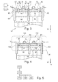
- the figure 7 represents in more detail the cell 66 placed in this row 120.
- the ground planes 80 and 92 of the cell 66 are both in direct electrical contact with this box 122.
- the figure 8 represents in more detail the cell 124.
- This cell 124 is identical to the cell 30, except that the transistor 102 is replaced by a transistor 126.
- the transistor 126 is identical to the transistor 102, except that the ground plane 106 is replaced by a ground plane 128 of opposite doping.
- ground planes 104 and 128 thus have the same doping, of the opposite type to the doping of the box 122.
- the ground planes 104 and 128 of the cell 124 can be polarized so as to electrically isolate the transistors 100 and 126 of the transistors 68 and 70 of the adjacent cell 66 ( Fig. 7 ).
- the single box 122 makes it possible to place, within the row 120, standard cells contiguous to each other and having different type of threshold voltages.
- the figure 9 represents a cell 140 adapted to replace the cell 124.
- This cell 140 is identical to the cell 124, except that the transistor 126 is replaced by a transistor 141.
- the transistor 141 is identical to the transistor 126 except that the ground plane 128 is replaced. by a plane of mass 142 of opposite doping.
- this ground plane 142 is identical to the ground plane 106.
- the ground planes 104 and 142 have opposite type dopings.
- the doping of the ground plane 142 is of the same type as the doping of the caisson 122.
- the transistor 100 can be electrically isolated from the cell 66 (FIG. Fig. 7 ) contiguous in the same row 120, but the ground plane 142 of the cell 140 is not.
- This ground plane 142 is here able to be brought to the same electrical potential as the ground plane 80 of the adjoining cell 66, via the caisson 122.
- the cell 140 is said to be partially isolated.
- the figure 10 represents a row 150 of cells, able to replace the row 52 or 120.
- This row 150 contains standard cells and a clock tree cell 152.
- This row 150 is identical to the row 120, except that one half of the box 122, situated only under the cell 152, is replaced by a box 154, of opposite doping.
- This box 154 is, for example, identical to the box 62, except that it extends only under the cell 152. Under the cell 152, these boxes 122 and 154 extend parallel to one another in the direction X.
- These boxes 122 and 154 are here separated by a deep isolation trench 155, identical to the trench 64 except that it extends only in the cell 152.
- the network 132 is replaced by a network 156, identical to the network 132, except that it is electrically connected to the sockets 47, 48 and to the outlets of the cell 152.
- the figure 11 represents in more detail the cell 152.
- This cell 152 has transistors whose ground planes have a doping of the same type.
- This cell 152 is, for example, identical to the cell 124.
- the operation of the cell 152 is identical to the operation of the cell 140, except that the step 206 is replaced by a step 208, represented in dotted lines on the figure 5 .
- This step is identical to step 206, except that the electric polarization V PFET_CK2 is applied on the ground plane 128 to reverse bias the pn junction formed between the ground plane 128 and the box 122.
- Circuit 2 illustrated at figure 1 may be different from the illustrated example, and may include in particular a greater number of logical and / or synchronous elements.
- the assembly 20 may comprise more than one IN input and / or more than one OUT output.
- the rows of the block 6 may have a different configuration.
- the rows may be arranged in a so-called un-returned configuration ("regular" in English).
- the boxes can be arranged identically in each of the rows of the block 6.
- the cells of a block placed next to each other do not form parallel rows.
- the height cells in the Y direction are not the same for all cells in the same block of contiguous cells.
- Common boxes with several contiguous cells are not necessarily straight and can adopt a wide variety of shapes. Such an arrangement of cells is found for example in logic circuits. However, what has been previously described in the case where the cells are aligned in rows, also applies to those cases where such rows do not exist.
- the cell 30 may have a function other than delay.
- the cell 30 is, for example, adapted to amplify the clock input signal.
- the substrate 50 may have n-type doping.
- Source 53 can be omitted.
- the network 51 is electrically connected to a power source located outside the circuit 2.
- the trench 64 of the cells 124 and / or 152 is replaced by a short isolation trench, for example identical to the trench 91.
- This short trench makes it possible to isolate the active layer 72 from each of the transistors 100 and 126 but does not electrically isolate the ground planes 104 and 128 from each other. In this case, these ground planes 104 and 128 may be biased at the same electrical potential using a single contact point. .
- One or the other of the outlets 55 or 130 can then be omitted.
- the cell 66 may comprise more than two transistors 68 and 70.
- the transistors of the standard cells may have an intermediate threshold voltage (RVT).
- the respective ground planes of these transistors can be replaced by ground planes having opposite type doping (p-type doping under nMOS and n-type under pMOS).
- the doping types of the ground planes 80 and 92 of the cell 66 are permuted.
- the doping types of the ground planes 104 and 106 of the cell 30, as well as the caissons 60 and 62 are then permuted.
- the bias V PFET is then chosen equal to a supply voltage VDD of the circuit 2 in nominal polarization.
- the polarizations V PFET_CK1 and V NFET_CK1 are, in this case, chosen, respectively, less than or equal to the voltage VDD and greater than or equal to the ground GND.
- the source 82 and the drain 84 are not formed on the layer 72, but are formed inside this layer 72, or inside and above this layer 72, for example by epitaxy .
- the row 120 including the box 122, can be used within the block 6 instead of the row 38. The same goes for the row 150.
- the box 122 may have a p-type doping.
- the ground planes 104 and 128 of the cells 124 and 152 are replaced by ground planes with opposite types of doping.
- the polarizations V PFET_CK2 and V NFET_CK2 are, in this case, chosen greater than or equal to the mass GND.
- V NFET and V PFET polarizations can be modulated by a variable electrical potential ⁇ V, for example to apply inverse or direct type polarizations (respectively RBB and FBB, for "reverse back biasing” and “forward back biasing” in English language). It is the same for the polarizations V PFET_CK1 and V NFET_CK1 , and V PFET_CK2 and V NFET_CK2 .
Landscapes
- Engineering & Computer Science (AREA)
- Physics & Mathematics (AREA)
- Mathematical Physics (AREA)
- General Engineering & Computer Science (AREA)
- Computer Hardware Design (AREA)
- Computing Systems (AREA)
- Computer Networks & Wireless Communication (AREA)
- Electromagnetism (AREA)
- General Physics & Mathematics (AREA)
- Radar, Positioning & Navigation (AREA)
- Automation & Control Theory (AREA)
- Design And Manufacture Of Integrated Circuits (AREA)
- Semiconductor Integrated Circuits (AREA)
- Metal-Oxide And Bipolar Metal-Oxide Semiconductor Integrated Circuits (AREA)
Applications Claiming Priority (1)
| Application Number | Priority Date | Filing Date | Title |
|---|---|---|---|
| FR1262811A FR3000295B1 (fr) | 2012-12-26 | 2012-12-26 | Circuit integre comprenant une cellule d'arbre d'horloge |
Publications (3)
| Publication Number | Publication Date |
|---|---|
| EP2750179A2 true EP2750179A2 (de) | 2014-07-02 |
| EP2750179A3 EP2750179A3 (de) | 2017-11-29 |
| EP2750179B1 EP2750179B1 (de) | 2021-06-16 |
Family
ID=48856668
Family Applications (1)
| Application Number | Title | Priority Date | Filing Date |
|---|---|---|---|
| EP13198069.0A Active EP2750179B1 (de) | 2012-12-26 | 2013-12-18 | Integrierter Schaltkreis, der eine Taktbaumzelle umfasst |
Country Status (3)
| Country | Link |
|---|---|
| US (1) | US8937505B2 (de) |
| EP (1) | EP2750179B1 (de) |
| FR (1) | FR3000295B1 (de) |
Families Citing this family (4)
| Publication number | Priority date | Publication date | Assignee | Title |
|---|---|---|---|---|
| US9842184B2 (en) * | 2015-09-11 | 2017-12-12 | Globalfoundries Inc. | Method, apparatus and system for using hybrid library track design for SOI technology |
| US9716155B2 (en) | 2015-12-09 | 2017-07-25 | International Business Machines Corporation | Vertical field-effect-transistors having multiple threshold voltages |
| US10096602B1 (en) * | 2017-03-15 | 2018-10-09 | Globalfoundries Singapore Pte. Ltd. | MTP memory for SOI process |
| CN111898334B (zh) * | 2020-08-04 | 2022-02-01 | 深圳比特微电子科技有限公司 | 用于系统级芯片设计的标准单元及应用其的数据处理单元、运算芯片和计算设备 |
Citations (2)
| Publication number | Priority date | Publication date | Assignee | Title |
|---|---|---|---|---|
| US20060027877A1 (en) | 2004-08-05 | 2006-02-09 | Kabushiki Kaisha Toshiba | Semiconductor device with triple-well region |
| WO2012160071A1 (fr) | 2011-05-24 | 2012-11-29 | Commissariat à l'énergie atomique et aux énergies alternatives | Circuit integre realise en soi comprenant des cellules adjacentes de differents types |
Family Cites Families (1)
| Publication number | Priority date | Publication date | Assignee | Title |
|---|---|---|---|---|
| US6952117B2 (en) * | 2002-03-08 | 2005-10-04 | Micron Technology Inc. | Distributed clock generator for semiconductor devices and related method of operating semiconductor devices |
-
2012
- 2012-12-26 FR FR1262811A patent/FR3000295B1/fr not_active Expired - Fee Related
-
2013
- 2013-12-18 EP EP13198069.0A patent/EP2750179B1/de active Active
- 2013-12-19 US US14/134,081 patent/US8937505B2/en active Active
Patent Citations (2)
| Publication number | Priority date | Publication date | Assignee | Title |
|---|---|---|---|---|
| US20060027877A1 (en) | 2004-08-05 | 2006-02-09 | Kabushiki Kaisha Toshiba | Semiconductor device with triple-well region |
| WO2012160071A1 (fr) | 2011-05-24 | 2012-11-29 | Commissariat à l'énergie atomique et aux énergies alternatives | Circuit integre realise en soi comprenant des cellules adjacentes de differents types |
Non-Patent Citations (2)
| Title |
|---|
| JEAN-PHILIPPE NOEL ET AL.: "Multi-VT UTBB FDSOI device architectures for low-power CMOS circuit", IEEE TRANSACTIONS ON ELECTRON DEVICES, vol. 58, August 2011 (2011-08-01), pages 2473 - 2482, XP011336322, DOI: doi:10.1109/TED.2011.2155658 |
| P. FLATRESSE ET AL.: "Planar fully depleted silicon technology to design competitive SOC at 28nm and beyond", STMICROELECTRONICS, 2012, Retrieved from the Internet <URL:www.soiconsortium.org> |
Also Published As
| Publication number | Publication date |
|---|---|
| FR3000295B1 (fr) | 2015-02-27 |
| EP2750179A3 (de) | 2017-11-29 |
| US20140176228A1 (en) | 2014-06-26 |
| US8937505B2 (en) | 2015-01-20 |
| FR3000295A1 (fr) | 2014-06-27 |
| EP2750179B1 (de) | 2021-06-16 |
Similar Documents
| Publication | Publication Date | Title |
|---|---|---|
| EP2750180B1 (de) | Integrierter Schaltkreis, der eine Taktbaumzelle umfasst | |
| FR2953641A1 (fr) | Circuit de transistors homogenes sur seoi avec grille de controle arriere enterree sous la couche isolante | |
| EP2415079B1 (de) | Integrierter soi-schaltkreis mit transistoren mit separaten schwellenspannungen | |
| EP2685500A1 (de) | Integrierte Schaltung auf SOI mit einem Thyristor (SCR) zum Schutz vor elektrostatischen Entladungen | |
| FR2975828A1 (fr) | Circuit integre realise en soi comprenant des cellules adjacentes de differents types | |
| FR2980035A1 (fr) | Circuit integre realise en soi comprenant des cellules adjacentes de differents types | |
| FR2957186A1 (fr) | Cellule memoire de type sram | |
| FR3007577A1 (fr) | Transistors avec differents niveaux de tensions de seuil et absence de distorsions entre nmos et pmos | |
| FR2980640A1 (fr) | Circuit integre en technologie fdsoi avec partage de caisson et moyens de polarisation des plans de masse de dopage opposes presents dans un meme caisson | |
| FR3005203A1 (fr) | Circuit integre sur soi comprenant un transistor de protection contre des decharges electrostatiques | |
| FR3085536A1 (fr) | Dispositif cfet et procede de fabrication d'un tel dispositif | |
| EP2685501A1 (de) | Integrierter SOI-Schaltkreis, der einen darunterliegenden Schutztransistor umfasst | |
| EP2750179B1 (de) | Integrierter Schaltkreis, der eine Taktbaumzelle umfasst | |
| FR2957193A1 (fr) | Cellule a chemin de donnees sur substrat seoi avec grille de controle arriere enterree sous la couche isolante | |
| EP2685499A1 (de) | Integrierter SOI-Schaltkreis, der einen Triac zum Schutz gegen elektrostatische Entladungen umfasst | |
| EP2784817A1 (de) | Verfahren zum Steuern einer integrierten Schaltung | |
| EP2947689B1 (de) | Photonischer cmos-wechselrichter | |
| EP2775529A2 (de) | Transistor mit Tunneleffekt | |
| EP2685502A1 (de) | Integrierter SOI-Schaltkreis, der einen bipolaren Transistor mit Isolationsrinnen unterschiedlicher Tiefe umfasst | |
| FR3048304A1 (fr) | Puce electronique a transistors a grilles avant et arriere | |
| WO2014057112A1 (fr) | Circuit integre comportant des transistors avec des tensions de seuil differentes | |
| EP3163622B1 (de) | Lichtempfindliche logikzelle zur beleuchtung von der vorderseite | |
| FR3003690A1 (fr) | Circuit integre sur soi comprenant une matrice de cellules de memoire vive et un circuit peripherique accole | |
| FR2989218A1 (fr) | Procede de realisation d'un dispositif electronique par assemblage de blocs semi-conducteurs et dispositif correspondant | |
| FR3056372A1 (fr) | Circuit integre comprenant des cellules equilibrees en bordure de zone active |
Legal Events
| Date | Code | Title | Description |
|---|---|---|---|
| 17P | Request for examination filed |
Effective date: 20131218 |
|
| AK | Designated contracting states |
Kind code of ref document: A2 Designated state(s): AL AT BE BG CH CY CZ DE DK EE ES FI FR GB GR HR HU IE IS IT LI LT LU LV MC MK MT NL NO PL PT RO RS SE SI SK SM TR |
|
| AX | Request for extension of the european patent |
Extension state: BA ME |
|
| PUAI | Public reference made under article 153(3) epc to a published international application that has entered the european phase |
Free format text: ORIGINAL CODE: 0009012 |
|
| PUAL | Search report despatched |
Free format text: ORIGINAL CODE: 0009013 |
|
| AK | Designated contracting states |
Kind code of ref document: A3 Designated state(s): AL AT BE BG CH CY CZ DE DK EE ES FI FR GB GR HR HU IE IS IT LI LT LU LV MC MK MT NL NO PL PT RO RS SE SI SK SM TR |
|
| AX | Request for extension of the european patent |
Extension state: BA ME |
|
| RIC1 | Information provided on ipc code assigned before grant |
Ipc: H01L 29/786 20060101ALN20171026BHEP Ipc: H01L 27/118 20060101ALI20171026BHEP Ipc: H01L 21/84 20060101AFI20171026BHEP Ipc: H03K 19/177 20060101ALI20171026BHEP Ipc: H01L 27/12 20060101ALI20171026BHEP |
|
| STAA | Information on the status of an ep patent application or granted ep patent |
Free format text: STATUS: REQUEST FOR EXAMINATION WAS MADE |
|
| R17P | Request for examination filed (corrected) |
Effective date: 20180308 |
|
| RBV | Designated contracting states (corrected) |
Designated state(s): AL AT BE BG CH CY CZ DE DK EE ES FI FR GB GR HR HU IE IS IT LI LT LU LV MC MK MT NL NO PL PT RO RS SE SI SK SM TR |
|
| RIC1 | Information provided on ipc code assigned before grant |
Ipc: H03K 19/17736 20200101ALI20201123BHEP Ipc: H01L 27/118 20060101ALI20201123BHEP Ipc: H01L 29/786 20060101ALN20201123BHEP Ipc: H01L 27/12 20060101ALI20201123BHEP Ipc: H01L 21/84 20060101AFI20201123BHEP |
|
| GRAP | Despatch of communication of intention to grant a patent |
Free format text: ORIGINAL CODE: EPIDOSNIGR1 |
|
| STAA | Information on the status of an ep patent application or granted ep patent |
Free format text: STATUS: GRANT OF PATENT IS INTENDED |
|
| INTG | Intention to grant announced |
Effective date: 20210112 |
|
| RIC1 | Information provided on ipc code assigned before grant |
Ipc: H01L 27/12 20060101ALI20201210BHEP Ipc: H03K 19/17736 20200101ALI20201210BHEP Ipc: H01L 27/118 20060101ALI20201210BHEP Ipc: H01L 29/786 20060101ALN20201210BHEP Ipc: H01L 21/84 20060101AFI20201210BHEP |
|
| GRAS | Grant fee paid |
Free format text: ORIGINAL CODE: EPIDOSNIGR3 |
|
| GRAA | (expected) grant |
Free format text: ORIGINAL CODE: 0009210 |
|
| STAA | Information on the status of an ep patent application or granted ep patent |
Free format text: STATUS: THE PATENT HAS BEEN GRANTED |
|
| AK | Designated contracting states |
Kind code of ref document: B1 Designated state(s): AL AT BE BG CH CY CZ DE DK EE ES FI FR GB GR HR HU IE IS IT LI LT LU LV MC MK MT NL NO PL PT RO RS SE SI SK SM TR |
|
| REG | Reference to a national code |
Ref country code: GB Ref legal event code: FG4D Free format text: NOT ENGLISH |
|
| REG | Reference to a national code |
Ref country code: CH Ref legal event code: EP |
|
| REG | Reference to a national code |
Ref country code: DE Ref legal event code: R096 Ref document number: 602013077937 Country of ref document: DE |
|
| REG | Reference to a national code |
Ref country code: AT Ref legal event code: REF Ref document number: 1403039 Country of ref document: AT Kind code of ref document: T Effective date: 20210715 |
|
| REG | Reference to a national code |
Ref country code: IE Ref legal event code: FG4D Free format text: LANGUAGE OF EP DOCUMENT: FRENCH |
|
| REG | Reference to a national code |
Ref country code: LT Ref legal event code: MG9D |
|
| PG25 | Lapsed in a contracting state [announced via postgrant information from national office to epo] |
Ref country code: FI Free format text: LAPSE BECAUSE OF FAILURE TO SUBMIT A TRANSLATION OF THE DESCRIPTION OR TO PAY THE FEE WITHIN THE PRESCRIBED TIME-LIMIT Effective date: 20210616 Ref country code: LT Free format text: LAPSE BECAUSE OF FAILURE TO SUBMIT A TRANSLATION OF THE DESCRIPTION OR TO PAY THE FEE WITHIN THE PRESCRIBED TIME-LIMIT Effective date: 20210616 Ref country code: BG Free format text: LAPSE BECAUSE OF FAILURE TO SUBMIT A TRANSLATION OF THE DESCRIPTION OR TO PAY THE FEE WITHIN THE PRESCRIBED TIME-LIMIT Effective date: 20210916 Ref country code: HR Free format text: LAPSE BECAUSE OF FAILURE TO SUBMIT A TRANSLATION OF THE DESCRIPTION OR TO PAY THE FEE WITHIN THE PRESCRIBED TIME-LIMIT Effective date: 20210616 |
|
| REG | Reference to a national code |
Ref country code: AT Ref legal event code: MK05 Ref document number: 1403039 Country of ref document: AT Kind code of ref document: T Effective date: 20210616 |
|
| REG | Reference to a national code |
Ref country code: NL Ref legal event code: MP Effective date: 20210616 |
|
| PG25 | Lapsed in a contracting state [announced via postgrant information from national office to epo] |
Ref country code: NO Free format text: LAPSE BECAUSE OF FAILURE TO SUBMIT A TRANSLATION OF THE DESCRIPTION OR TO PAY THE FEE WITHIN THE PRESCRIBED TIME-LIMIT Effective date: 20210916 Ref country code: GR Free format text: LAPSE BECAUSE OF FAILURE TO SUBMIT A TRANSLATION OF THE DESCRIPTION OR TO PAY THE FEE WITHIN THE PRESCRIBED TIME-LIMIT Effective date: 20210917 Ref country code: LV Free format text: LAPSE BECAUSE OF FAILURE TO SUBMIT A TRANSLATION OF THE DESCRIPTION OR TO PAY THE FEE WITHIN THE PRESCRIBED TIME-LIMIT Effective date: 20210616 Ref country code: RS Free format text: LAPSE BECAUSE OF FAILURE TO SUBMIT A TRANSLATION OF THE DESCRIPTION OR TO PAY THE FEE WITHIN THE PRESCRIBED TIME-LIMIT Effective date: 20210616 Ref country code: SE Free format text: LAPSE BECAUSE OF FAILURE TO SUBMIT A TRANSLATION OF THE DESCRIPTION OR TO PAY THE FEE WITHIN THE PRESCRIBED TIME-LIMIT Effective date: 20210616 |
|
| PG25 | Lapsed in a contracting state [announced via postgrant information from national office to epo] |
Ref country code: PT Free format text: LAPSE BECAUSE OF FAILURE TO SUBMIT A TRANSLATION OF THE DESCRIPTION OR TO PAY THE FEE WITHIN THE PRESCRIBED TIME-LIMIT Effective date: 20211018 Ref country code: RO Free format text: LAPSE BECAUSE OF FAILURE TO SUBMIT A TRANSLATION OF THE DESCRIPTION OR TO PAY THE FEE WITHIN THE PRESCRIBED TIME-LIMIT Effective date: 20210616 Ref country code: NL Free format text: LAPSE BECAUSE OF FAILURE TO SUBMIT A TRANSLATION OF THE DESCRIPTION OR TO PAY THE FEE WITHIN THE PRESCRIBED TIME-LIMIT Effective date: 20210616 Ref country code: ES Free format text: LAPSE BECAUSE OF FAILURE TO SUBMIT A TRANSLATION OF THE DESCRIPTION OR TO PAY THE FEE WITHIN THE PRESCRIBED TIME-LIMIT Effective date: 20210616 Ref country code: AT Free format text: LAPSE BECAUSE OF FAILURE TO SUBMIT A TRANSLATION OF THE DESCRIPTION OR TO PAY THE FEE WITHIN THE PRESCRIBED TIME-LIMIT Effective date: 20210616 Ref country code: EE Free format text: LAPSE BECAUSE OF FAILURE TO SUBMIT A TRANSLATION OF THE DESCRIPTION OR TO PAY THE FEE WITHIN THE PRESCRIBED TIME-LIMIT Effective date: 20210616 Ref country code: CZ Free format text: LAPSE BECAUSE OF FAILURE TO SUBMIT A TRANSLATION OF THE DESCRIPTION OR TO PAY THE FEE WITHIN THE PRESCRIBED TIME-LIMIT Effective date: 20210616 Ref country code: SK Free format text: LAPSE BECAUSE OF FAILURE TO SUBMIT A TRANSLATION OF THE DESCRIPTION OR TO PAY THE FEE WITHIN THE PRESCRIBED TIME-LIMIT Effective date: 20210616 Ref country code: SM Free format text: LAPSE BECAUSE OF FAILURE TO SUBMIT A TRANSLATION OF THE DESCRIPTION OR TO PAY THE FEE WITHIN THE PRESCRIBED TIME-LIMIT Effective date: 20210616 |
|
| PG25 | Lapsed in a contracting state [announced via postgrant information from national office to epo] |
Ref country code: PL Free format text: LAPSE BECAUSE OF FAILURE TO SUBMIT A TRANSLATION OF THE DESCRIPTION OR TO PAY THE FEE WITHIN THE PRESCRIBED TIME-LIMIT Effective date: 20210616 |
|
| REG | Reference to a national code |
Ref country code: DE Ref legal event code: R097 Ref document number: 602013077937 Country of ref document: DE |
|
| PLBE | No opposition filed within time limit |
Free format text: ORIGINAL CODE: 0009261 |
|
| STAA | Information on the status of an ep patent application or granted ep patent |
Free format text: STATUS: NO OPPOSITION FILED WITHIN TIME LIMIT |
|
| PG25 | Lapsed in a contracting state [announced via postgrant information from national office to epo] |
Ref country code: DK Free format text: LAPSE BECAUSE OF FAILURE TO SUBMIT A TRANSLATION OF THE DESCRIPTION OR TO PAY THE FEE WITHIN THE PRESCRIBED TIME-LIMIT Effective date: 20210616 |
|
| 26N | No opposition filed |
Effective date: 20220317 |
|
| PG25 | Lapsed in a contracting state [announced via postgrant information from national office to epo] |
Ref country code: AL Free format text: LAPSE BECAUSE OF FAILURE TO SUBMIT A TRANSLATION OF THE DESCRIPTION OR TO PAY THE FEE WITHIN THE PRESCRIBED TIME-LIMIT Effective date: 20210616 |
|
| PG25 | Lapsed in a contracting state [announced via postgrant information from national office to epo] |
Ref country code: MC Free format text: LAPSE BECAUSE OF FAILURE TO SUBMIT A TRANSLATION OF THE DESCRIPTION OR TO PAY THE FEE WITHIN THE PRESCRIBED TIME-LIMIT Effective date: 20210616 Ref country code: IT Free format text: LAPSE BECAUSE OF FAILURE TO SUBMIT A TRANSLATION OF THE DESCRIPTION OR TO PAY THE FEE WITHIN THE PRESCRIBED TIME-LIMIT Effective date: 20210616 |
|
| REG | Reference to a national code |
Ref country code: CH Ref legal event code: PL |
|
| GBPC | Gb: european patent ceased through non-payment of renewal fee |
Effective date: 20211218 |
|
| REG | Reference to a national code |
Ref country code: BE Ref legal event code: MM Effective date: 20211231 |
|
| PG25 | Lapsed in a contracting state [announced via postgrant information from national office to epo] |
Ref country code: LU Free format text: LAPSE BECAUSE OF NON-PAYMENT OF DUE FEES Effective date: 20211218 Ref country code: IE Free format text: LAPSE BECAUSE OF NON-PAYMENT OF DUE FEES Effective date: 20211218 Ref country code: GB Free format text: LAPSE BECAUSE OF NON-PAYMENT OF DUE FEES Effective date: 20211218 |
|
| PG25 | Lapsed in a contracting state [announced via postgrant information from national office to epo] |
Ref country code: FR Free format text: LAPSE BECAUSE OF NON-PAYMENT OF DUE FEES Effective date: 20211231 Ref country code: BE Free format text: LAPSE BECAUSE OF NON-PAYMENT OF DUE FEES Effective date: 20211231 |
|
| PG25 | Lapsed in a contracting state [announced via postgrant information from national office to epo] |
Ref country code: LI Free format text: LAPSE BECAUSE OF NON-PAYMENT OF DUE FEES Effective date: 20211231 Ref country code: CH Free format text: LAPSE BECAUSE OF NON-PAYMENT OF DUE FEES Effective date: 20211231 |
|
| PG25 | Lapsed in a contracting state [announced via postgrant information from national office to epo] |
Ref country code: HU Free format text: LAPSE BECAUSE OF FAILURE TO SUBMIT A TRANSLATION OF THE DESCRIPTION OR TO PAY THE FEE WITHIN THE PRESCRIBED TIME-LIMIT; INVALID AB INITIO Effective date: 20131218 |
|
| PG25 | Lapsed in a contracting state [announced via postgrant information from national office to epo] |
Ref country code: CY Free format text: LAPSE BECAUSE OF FAILURE TO SUBMIT A TRANSLATION OF THE DESCRIPTION OR TO PAY THE FEE WITHIN THE PRESCRIBED TIME-LIMIT Effective date: 20210616 |
|
| PG25 | Lapsed in a contracting state [announced via postgrant information from national office to epo] |
Ref country code: MK Free format text: LAPSE BECAUSE OF FAILURE TO SUBMIT A TRANSLATION OF THE DESCRIPTION OR TO PAY THE FEE WITHIN THE PRESCRIBED TIME-LIMIT Effective date: 20210616 |
|
| PG25 | Lapsed in a contracting state [announced via postgrant information from national office to epo] |
Ref country code: TR Free format text: LAPSE BECAUSE OF FAILURE TO SUBMIT A TRANSLATION OF THE DESCRIPTION OR TO PAY THE FEE WITHIN THE PRESCRIBED TIME-LIMIT Effective date: 20210616 |
|
| PG25 | Lapsed in a contracting state [announced via postgrant information from national office to epo] |
Ref country code: MT Free format text: LAPSE BECAUSE OF FAILURE TO SUBMIT A TRANSLATION OF THE DESCRIPTION OR TO PAY THE FEE WITHIN THE PRESCRIBED TIME-LIMIT Effective date: 20210616 |
|
| REG | Reference to a national code |
Ref country code: DE Ref legal event code: R079 Ref document number: 602013077937 Country of ref document: DE Free format text: PREVIOUS MAIN CLASS: H01L0021840000 Ipc: H10D0086010000 |
|
| PGFP | Annual fee paid to national office [announced via postgrant information from national office to epo] |
Ref country code: DE Payment date: 20251126 Year of fee payment: 13 |