EP2755005A2 - Ausgangsspezifizierungskalibrierungsvorrichtung für kapazitiven Drucksensor - Google Patents
Ausgangsspezifizierungskalibrierungsvorrichtung für kapazitiven Drucksensor Download PDFInfo
- Publication number
- EP2755005A2 EP2755005A2 EP13187300.2A EP13187300A EP2755005A2 EP 2755005 A2 EP2755005 A2 EP 2755005A2 EP 13187300 A EP13187300 A EP 13187300A EP 2755005 A2 EP2755005 A2 EP 2755005A2
- Authority
- EP
- European Patent Office
- Prior art keywords
- output
- output specification
- capacitance
- pressure sensor
- calibrating apparatus
- Prior art date
- Legal status (The legal status is an assumption and is not a legal conclusion. Google has not performed a legal analysis and makes no representation as to the accuracy of the status listed.)
- Withdrawn
Links
- 230000008859 change Effects 0.000 claims description 11
- 238000012937 correction Methods 0.000 claims description 3
- 238000010586 diagram Methods 0.000 description 10
- 239000000758 substrate Substances 0.000 description 7
- 230000003111 delayed effect Effects 0.000 description 5
- 238000009530 blood pressure measurement Methods 0.000 description 3
- 230000010354 integration Effects 0.000 description 3
- 238000000034 method Methods 0.000 description 3
- 238000012986 modification Methods 0.000 description 3
- 230000004048 modification Effects 0.000 description 3
- 238000004088 simulation Methods 0.000 description 3
- 239000003990 capacitor Substances 0.000 description 2
- 238000005259 measurement Methods 0.000 description 2
- 230000004044 response Effects 0.000 description 2
- 230000001052 transient effect Effects 0.000 description 2
- 238000009825 accumulation Methods 0.000 description 1
- 230000003321 amplification Effects 0.000 description 1
- 238000004891 communication Methods 0.000 description 1
- 238000010276 construction Methods 0.000 description 1
- 238000007599 discharging Methods 0.000 description 1
- 230000000694 effects Effects 0.000 description 1
- 238000005516 engineering process Methods 0.000 description 1
- 238000003199 nucleic acid amplification method Methods 0.000 description 1
- 230000009467 reduction Effects 0.000 description 1
- 238000011160 research Methods 0.000 description 1
- 238000012546 transfer Methods 0.000 description 1
- 238000009966 trimming Methods 0.000 description 1
Images




Classifications
-
- G—PHYSICS
- G01—MEASURING; TESTING
- G01L—MEASURING FORCE, STRESS, TORQUE, WORK, MECHANICAL POWER, MECHANICAL EFFICIENCY, OR FLUID PRESSURE
- G01L27/00—Testing or calibrating of apparatus for measuring fluid pressure
- G01L27/002—Calibrating, i.e. establishing true relation between transducer output value and value to be measured, zeroing, linearising or span error determination
-
- G—PHYSICS
- G01—MEASURING; TESTING
- G01D—MEASURING NOT SPECIALLY ADAPTED FOR A SPECIFIC VARIABLE; ARRANGEMENTS FOR MEASURING TWO OR MORE VARIABLES NOT COVERED IN A SINGLE OTHER SUBCLASS; TARIFF METERING APPARATUS; MEASURING OR TESTING NOT OTHERWISE PROVIDED FOR
- G01D18/00—Testing or calibrating apparatus or arrangements provided for in groups G01D1/00 - G01D15/00
- G01D18/008—Testing or calibrating apparatus or arrangements provided for in groups G01D1/00 - G01D15/00 with calibration coefficients stored in memory
-
- G—PHYSICS
- G01—MEASURING; TESTING
- G01D—MEASURING NOT SPECIALLY ADAPTED FOR A SPECIFIC VARIABLE; ARRANGEMENTS FOR MEASURING TWO OR MORE VARIABLES NOT COVERED IN A SINGLE OTHER SUBCLASS; TARIFF METERING APPARATUS; MEASURING OR TESTING NOT OTHERWISE PROVIDED FOR
- G01D5/00—Mechanical means for transferring the output of a sensing member; Means for converting the output of a sensing member to another variable where the form or nature of the sensing member does not constrain the means for converting; Transducers not specially adapted for a specific variable
- G01D5/12—Mechanical means for transferring the output of a sensing member; Means for converting the output of a sensing member to another variable where the form or nature of the sensing member does not constrain the means for converting; Transducers not specially adapted for a specific variable using electric or magnetic means
- G01D5/14—Mechanical means for transferring the output of a sensing member; Means for converting the output of a sensing member to another variable where the form or nature of the sensing member does not constrain the means for converting; Transducers not specially adapted for a specific variable using electric or magnetic means influencing the magnitude of a current or voltage
- G01D5/24—Mechanical means for transferring the output of a sensing member; Means for converting the output of a sensing member to another variable where the form or nature of the sensing member does not constrain the means for converting; Transducers not specially adapted for a specific variable using electric or magnetic means influencing the magnitude of a current or voltage by varying capacitance
-
- G—PHYSICS
- G01—MEASURING; TESTING
- G01L—MEASURING FORCE, STRESS, TORQUE, WORK, MECHANICAL POWER, MECHANICAL EFFICIENCY, OR FLUID PRESSURE
- G01L9/00—Measuring steady of quasi-steady pressure of fluid or fluent solid material by electric or magnetic pressure-sensitive elements; Transmitting or indicating the displacement of mechanical pressure-sensitive elements, used to measure the steady or quasi-steady pressure of a fluid or fluent solid material, by electric or magnetic means
- G01L9/0041—Transmitting or indicating the displacement of flexible diaphragms
- G01L9/0072—Transmitting or indicating the displacement of flexible diaphragms using variations in capacitance
-
- G—PHYSICS
- G01—MEASURING; TESTING
- G01L—MEASURING FORCE, STRESS, TORQUE, WORK, MECHANICAL POWER, MECHANICAL EFFICIENCY, OR FLUID PRESSURE
- G01L9/00—Measuring steady of quasi-steady pressure of fluid or fluent solid material by electric or magnetic pressure-sensitive elements; Transmitting or indicating the displacement of mechanical pressure-sensitive elements, used to measure the steady or quasi-steady pressure of a fluid or fluent solid material, by electric or magnetic means
- G01L9/12—Measuring steady of quasi-steady pressure of fluid or fluent solid material by electric or magnetic pressure-sensitive elements; Transmitting or indicating the displacement of mechanical pressure-sensitive elements, used to measure the steady or quasi-steady pressure of a fluid or fluent solid material, by electric or magnetic means by making use of variations in capacitance, i.e. electric circuits therefor
-
- G—PHYSICS
- G01—MEASURING; TESTING
- G01L—MEASURING FORCE, STRESS, TORQUE, WORK, MECHANICAL POWER, MECHANICAL EFFICIENCY, OR FLUID PRESSURE
- G01L9/00—Measuring steady of quasi-steady pressure of fluid or fluent solid material by electric or magnetic pressure-sensitive elements; Transmitting or indicating the displacement of mechanical pressure-sensitive elements, used to measure the steady or quasi-steady pressure of a fluid or fluent solid material, by electric or magnetic means
- G01L9/12—Measuring steady of quasi-steady pressure of fluid or fluent solid material by electric or magnetic pressure-sensitive elements; Transmitting or indicating the displacement of mechanical pressure-sensitive elements, used to measure the steady or quasi-steady pressure of a fluid or fluent solid material, by electric or magnetic means by making use of variations in capacitance, i.e. electric circuits therefor
- G01L9/125—Measuring steady of quasi-steady pressure of fluid or fluent solid material by electric or magnetic pressure-sensitive elements; Transmitting or indicating the displacement of mechanical pressure-sensitive elements, used to measure the steady or quasi-steady pressure of a fluid or fluent solid material, by electric or magnetic means by making use of variations in capacitance, i.e. electric circuits therefor with temperature compensating means
Definitions
- the following description relates to a pressure measurement technology, and more particularly, to an output specification calibrating apparatus for a capacitive pressure sensor.
- Pressure sensors convert mechanical deflection due to applied pressure into an electrical signal, and obtain the measurement of the pressure by measuring the output electrical signals.
- Korean Patent Publication No. 10-2001-0039983 (published on May 15, 2001 ) discloses a capacitive pressure sensor, which converts mechanical deflection into a capacitance, and measures a pressure by measuring the changes in capacitance.
- Capacitance pressure sensors have non-linearity characteristics with respect to an applied pressure, and are temperature-sensitive. Thus, to meet various demands of customers for output specifications of the capacitance pressure sensor, the output specifications need to be adjusted according to the individual customers' needs at the time of shipment. Thus, research on an output specification calibrating apparatus for a capacitive pressure sensor has been conducted in an attempt to meet a variety of desired output specifications of the capacitive pressure sensor.
- the following description relates to an output specification calibrating apparatus for a capacitive pressure sensor, which enables calibration of output specifications of the capacitive pressure sensor at the time of shipment, in an effort to meet various needs of customers for the output specifications.
- the following description also relates to an output specification calibrating apparatus for a capacitive pressure sensor, which enables easy calibration of output specifications of the capacitive pressure sensor in a software manner.
- an output specification calibrating apparatus for a capacitive pressure sensor including: an output control circuit configured to convert capacitance changes of a capacitance C p formed by a primary electrode of the capacitive pressure sensor and a capacitance C r formed by a reference electrode of the capacitive pressure sensor into an output voltage and output the output voltage; an output specification calibration element configured to comprise at least one output specification offset calibration element, an output specification non-linearity adjustment element, an output specification gain adjustment element, and an output specification temperature compensation element, each element configured to adjust a specification of an output of the output control circuit; a setting unit configured to set electrical property values of the output specification offset calibration element, the output specification non-linearity adjustment element and the output specification gain adjustment element; an external input interface configured to be connected to an external terminal for setting the electrical property values of the output specification offset calibration element, the output specification non-linearity adjustment element and the output specification gain adjustment element; and a temperature compensation circuit configured to set electrical property values of the output specification temperature compensation element.
- the output control circuit may be configured to include a switch unit configured to control charge and discharge operations of the capacitance C p formed by the primary electrode and the capacitance C r formed by the reference electrode, an integrator configured to receive currents discharged from the capacitance C p and the capacitance C r , output the received currents as an output voltage and continue to integrate an error correction signal until an error reaches zero, a power input unit configured to supply a constant power to the capacitance C p and the capacitance C r , and a feedback unit configured to amplify an output voltage from the integrator and feed the amplified output voltage back to the capacitance C p , the capacitance C r and the power input unit.
- a switch unit configured to control charge and discharge operations of the capacitance C p formed by the primary electrode and the capacitance C r formed by the reference electrode
- an integrator configured to receive currents discharged from the capacitance C p and the capacitance C r , output the received currents as
- the output specification offset calibration element may be configured to include two variable resistors R Lin1 and R Lin2 being connected in series between a power input V + and ground, branching off from a series connection contact point, and being connected to an input terminal of the power input unit to calibrate an input voltage offset.
- the setting unit may be configured to set resistances of the two variable resistors R Lin1 and R Lin2 as electrical property values.
- the output specification gain adjustment element may be configured to comprise a variable resistor ROF being connected to both an inversion input terminal of an amplifier and an output terminal of the amplifier, which amplifies the output voltage from the integrator, to adjust a gain of the amplifier.
- the setting unit may be configured to set a resistance of the variable resistor ROF as an electrical property value.
- the output specification temperature compensation element may be configured to include a variable resistor ROI being connected to an inversion input terminal of an amplifier and an output terminal of the integrator, to compensate for changes in an output voltage of the amplifier due to temperature change.
- the temperature compensation circuit may be configured to set a resistance of the variable resistor ROI as an electrical property value.
- the output specification non-linearity adjustment element may be configured to include a variable resistor R LinF being connected to both an output terminal of the feedback unit and an input terminal of the power input unit, and connecting a pair of the capacitance C p formed by the primary electrode of the capacitive pressure sensor and the capacitance C r formed by the reference electrode between the output terminal of the feedback unit and the variable resistor R LinF to improve non-linearity of the capacitive pressure sensor.
- a variable resistor R LinF being connected to both an output terminal of the feedback unit and an input terminal of the power input unit, and connecting a pair of the capacitance C p formed by the primary electrode of the capacitive pressure sensor and the capacitance C r formed by the reference electrode between the output terminal of the feedback unit and the variable resistor R LinF to improve non-linearity of the capacitive pressure sensor.
- the setting unit may be configured to set a resistance of the variable resistor R Linf as an electrical property value.
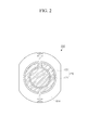
- FIGS. 1 and 2 are diagrams illustrating examples of a capacitive pressure sensor.
- the capacitive pressure sensor 100 may include a dielectric substrate 110 and an electrode pattern 120 in order to output convert mechanical deflection into electrostatic capacitance.
- the dielectric substrate 110 is where mechanical deflection occurs due to a pressure.
- the electrode pattern 120 formed on one surface of the dielectric substrate 110 includes a primary electrode 121 and a reference electrode 122, and is connected with an output specification calibrating apparatus via a lead unit (not illustrated).
- the main electrode 121 and the reference electrode 122 may work with a conductive plate, which is coupled on the other surface of the dielectric substrate 110, to form capacitance C p and capacitance Cr, respectively.
- FIG. 3A is a block diagram illustrating a configuration of an output specification calibrating apparatus for a capacitive pressure sensor according to an exemplary embodiment of the present invention.
- the output specification calibrating apparatus includes an output control circuit 200, one or more output specification offset calibration element 300, an output specification non-linearity adjustment element 310, an output specification gain adjustment element 320, an output specification temperature compensation element 330, a setting unit 400, an external input interface 500, and a temperature compensation circuit 600.
- the output control circuit 200 converts the capacitance changes of the capacitance C p formed by a primary electrode and the capacitance C r formed by a reference electrode into an output voltage and outputs it.
- the output specification offset calibration element 330, the output specification non-linearity adjustment element 310, the output specification gain adjustment element 320, and the output specification temperature compensation element 330 calibrate output specifications of the output control circuit 200 according to preset electrical property values.
- the output specification offset calibration element 300, the output specification non-linearity adjustment element 310, the output specification temperature compensation element 330 may be variable resistors for, respectively, offset calibration, non-linearity adjustment, gain adjustment and temperature compensation of the capacitive pressure sensor.
- the setting unit 400 sets the electrical property values of the output specification calibration element 300, the output specification non-linearity adjustment element 310 and the output specification gain adjustment element 320.
- the electrical property values set by the setting unit 400 may be resistances of the variable resistors for calibrating the offset, non-linearity and gain of the capacitive pressure sensor.
- the external input interface 500 is connected with an external terminal (not shown) to set the electrical property values of the output specification calibration element 300, the output specification non-linearity adjustment element 310 and the output specification gain adjustment element 320.
- the external input interface 500 may be a wired or wireless communication interface connected to an external device, such as a personal computer (PC) and a smartphone.
- PC personal computer
- the temperature compensation circuit 600 sets the electrical property value of the output specification temperature compensation element 330 to compensate for a temperature change such that a constant output specification of the output control circuit 200 can be maintained despite the changes in temperature, wherein the output specification of the output control circuit 200 varies with the electrical property values of the output specification offset calibration element 300, the output specification non-linearity adjustment element 310 and the output specification gain adjustment element 320, which are set by the setting unit 400 and changed according to temperature.
- the output of a capacitive pressure sensor has to be calibrated at the time of shipment so as to meet various needs of customers.
- the external terminal is connected to the external input interface 500 of the output specification calibrating apparatus for the capacitive pressure sensor, and software for calibrating the output specifications of the capacitive pressure sensor is executed for a user to manually input the electrical property values of the output specification offset calibration element 300, the output specification non-linearity adjustment element 310 and the output specification gain adjustment element 320.
- the setting unit 400 sets the electrical property values of the output specification offset calibration element 300, the output specification non-linearity adjustment element 310 and the output specification gain adjustment element 320.
- the setting unit 400 may store set resistances of the variable resistors. Then, the setting unit 400 reads in the stored resistances each time booting up and selects an electrical contact point of the variable resistors that is suitable to the read resistance, thereby setting the electrical property values of the output specification offset calibration element 300, the output specification non-linearity adjustment element 310 and the output specification gain adjustment element 320.
- the temperature compensation circuit 600 sets the electrical property value of the output specification temperature compensation element 330 to compensate for a temperature change such that a constant output specification of the output control circuit 200 can be maintained despite the changes in temperature, wherein the output specification of the output control circuit 200 varies with the electrical property values of the output specification offset calibration element 300, the output specification non-linearity adjustment element 310 and the output specification gain adjustment element 320, which are set by the setting unit 400 and changed according to temperature.
- the output specifications of the output control circuit 200 are calibrated according to the electrical property values of the output specification offset calibration element 300, the output specification non-linearity adjustment element 310, the output specification gain adjustment element 320 and the output specification temperature compensation element 330. Accordingly, it is possible to calibrate the non-linearity, offset and gain of the capacitive pressure sensor, which may vary with temperature when shipment, and to thereby meet various needs of customers for output specifications.
- the exemplary embodiments of the present invention allow convenient calibration of output specifications of the capacitive pressure sensor in a software manner.
- FIGS. 3B and 3C are circuit diagrams of the output specification offset calibration element and the output specification non-linearity adjustment element of FIG. 3A , each being implemented as a variable resistor, and the output specification gain adjustment element 320 and the output specification temperature compensation element 330 shown in FIG. 3A may also be implemented in the same manner as the output specification offset calibration element and the output specification non-linearity adjustment element.
- the output control circuit 200 includes a switch unit 210, an integrator 220, a power input unit 230, and a feedback unit 240.
- the switch unit 210 controls charging and discharging of the capacitance C p formed by the primary electrode and the capacitance C r formed by the reference electrode.
- the switch unit 210 includes six switches (including two P 1 switches which simultaneously turn “on” at the beginning of Phase 1 and enter in OFF state in Phase 2, two P 2 switches which simultaneously turn “on” at the beginning of Phase 2 that does not overlap Phase 1 and remain in OFF state in Phase 1, one P 1d switch which turns "on” after a predetermined period of time has elapsed since P1 switches turned “on” in Phase 1, and one P 2d switch which turns “on” after a predetermined period of time has elapsed since P 2 switches turned “on” in Phase 2).
- the capacitance C p formed by the primary electrode and the capacitance C r formed by the reference electrode are connected to each other in series between P 1 -P 2 switch pairs.
- a common terminal C com is formed at a branching point between the capacitance C p formed by the primary electrode and the capacitance C r formed by the reference electrode, and a terminal end of the common terminal C com is connected in parallel to the P 1d switch and the P 2d switch.
- the P 1 switch of the P 1 -P 2 switch pair to which the capacitance C r formed by the reference electrode is connected is connected to an output terminal of the power input unit 230, and the P 2 switch is connected to ground.
- the P 1 switch of the P 1 -P 2 switch pair to which the capacitance C p formed by the primary electrode is connected is connected to ground and the P 2 switch is connected to an output terminal of the feedback unit 240.
- the P 1d switch and the P 2d switch, which are connected to the common terminal C com in parallel, are connected to an inversion input terminal of the integrator 220 and ground, respectively.
- the integrator 220 receives currents discharged from the capacitance C p formed by the primary electrode and the capacitance C r formed by the reference electrode, and converts the currents into an output voltage V out and then outputs the voltage V out . In addition, the integrator 220 continues to integrate an error correction signal in a control loop until the error reaches zero.
- the integrator 220 includes an operational (OP) amplifier, an integration capacitor CF and a resistor R.
- a non-inversion input terminal of the operational amplifier is connected to ground via the resistor R for compensation of input bias current.
- An error in an integration result due to an input bias current may be reduced by equalizing a resistance between the two input terminals and ground.
- the inversion input terminal of the OP amplifier is connected to the P1d switch and receives currents discharged from the capacitance C p and the capacitance C r through the common terminal C com , wherein the capacitance C p is formed by the primary electrode of the capacitive pressure sensor and from the capacitance C r is formed by the reference electrode.
- the integration capacitor CF is connected between the inversion terminal of the OP amplifier and the output terminal thereof.
- An integrating error of the integrator 220 is in inverse proportion to an open direct-current (DC) gain of the OP amplifier.
- the use of OP amplifier may ensure sufficient accuracy even if only an input offset voltage is compensated.
- the power input unit 230 supplies a constant power load to the capacitance C p and the capacitance C r .
- the power input unit 230 may be a buffer in use for maintaining a constant output voltage regardless of the changes in load.
- the buffer supplies a constant power load to the capacitance C p formed by the primary electrode and the capacitance C r formed by the reference electrode.
- variable resistors R Lin1 and R Lin2 are used as output specification offset calibration elements 300 so as to calibrate an input voltage offset that is input to the power input unit 230.
- the two variable resistors R Lin1 and R Lin2 are connected in series between a power input V + and ground, branched off from a series connection contact point, and then connected to an input terminal of the power input unit 230.
- a non-inversion input terminal of the buffer is connected to the output terminal of the feedback unit 240.
- the buffer has an inversion terminal connected to its output terminal.
- An input voltage to the buffer which comes from the resistors R Lin1 and R Lin2 and the feedback unit 240, becomes V L , and an output voltage of the buffer is maintained to V L .
- the output voltage of the buffer is assigned to the capacitance C p formed by the primary electrode of the capacitive pressure sensor and the capacitance C r formed by the reference electrode by the switching operation of the switching unit 210, so that the capacitances C p and C r can be charged.
- Equation 7 the voltage V L input to the power input unit 230 may vary with resistances of the two variable resistors R Lin1 and R Lin2 .
- Equations 1 and 4 the output voltage from the integrator 220 is related to the voltage V L .
- an input voltage offset can be calibrated by setting, at the setting unit 400, the resistances of the two variable resistors R Lin1 and R Lin2 , which are the output specification offset calibration elements 300, when the capacitance pressure sensor is shipped, and thereby an output voltage of the capacitive pressure sensor can be calibrated.
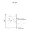
- FIG. 5A is a graph showing output specifications with respect to a change in pressure before and after offset calibration of an output specification calibrating apparatus for a capacitive pressure sensor according to an exemplary embodiment of the present invention.
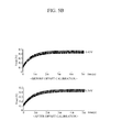
- FIG. 5B illustrates graphs showing results of a simulation for output specification with respect to time before and after offset calibration of the output specification calibrating apparatus for a capacitive pressure sensor according to the exemplary embodiment of the present invention.
- a resistance of the output specification offset calibration element 300 is set by the setting unit 400 to calibrate the output specification to be 0.5 V as shown in FIG. 5A .
- the feedback unit 240 amplifies the output voltage from the integrator 220 using an amplifier and feeds the amplified voltage back to the capacitance C p formed by the primary electrode of the capacitive pressure sensor, the capacitance C r formed by the reference electrode, and the power input unit 230.
- the voltage that has been output from the integrator 220 and amplified by the amplifier is assigned to capacitance C p and the capacitance C r by the switching operation of the switch unit 210.
- the amplifier assigns the output voltage, which has been output from the integrator and fed back, to the input terminal of the power input unit 230.
- a variable resistor ROF may be used as the output specification gain adjustment element 320 in order to calibrate a gain of the amplifier and a variable resistor ROI may be used as the output specification temperature compensation element 330 so as to calibrate the output specification according to temperature.
- An inversion input terminal of the amplifier is connected to an output terminal of the integrator 220 via the variable resistor ROI.
- Voltage formed between resistors Rof1 and Rof2 which are connected in series between a power input V + and ground is connected to a non-inversion input terminal of the amplifier.
- variable resistor ROF is connected between the inversion input terminal and the output terminal of the amplifier.
- the gain indicates how much an output voltage is amplified compared to an input voltage, and referring to Equation 1 which will be described later, the gain (a ratio of input voltage V out to output voltage V bdge ) may be represented as a ratio (ROI/ROF) of resistance of the variable resistor ROI to resistance of the variable resistor ROF.
- the gain may be calibrated by setting a resistance of the variable resistor ROF using the setting unit 400 before shipment of the capacitive pressure sensor, and thereby it is possible to calibrate the output voltage of the capacitive pressure sensor.
- the temperature compensation circuit 600 trims a resistance of the variable resistor ROI which is the output specification temperature compensation element 330, thereby compensating for the change in output voltage over temperature.
- the output specification non-linearity adjustment element 310 is connected between the output terminal of the feedback unit 240 and the input terminal of the power input unit 230.
- a variable resistor R LinF that is interposed between the power input unit 230 and the feedback unit 240 and is connected to the capacitance C p formed by the primary electrode of the capacitive pressure sensor and the capacitance C r formed by the reference electrode may be used as the output specification non-linearity adjustment element 310.
- FIG. 4 is a switching timing diagram for control of the output control circuit of the capacitive pressure sensor.
- the six switches (including two P 1 switches, two P 2 switches, one P 1d switch, and one P 2d switch) turn “on” or “off” in Phase 1 and Phase 2 which do not overlap each other.
- the two P 1 switches turn “on” at the beginning of Phase 1, and simultaneously enter in OFF state in Phase 2, and the P 1d switch turns “on” after a predetermined period of time has elapsed since the P 1 switches turned “on”.
- the two P 2 switches simultaneously turn “on” at the beginning of Phase 2 and simultaneously enter in OFF state in Phase 1, and the P 2d switch turns “on” after a predetermined period of time has elapsed since the P 2 switches turned “on”.
- Two non-overlapping phase control signals are output from an oscillator-driven gating circuit (not shown). In response to the two non-overlapping phase control signals, the six switches turn “on” or "off".
- the amplifier of the feedback unit 240 provides three independent variable adjustments.
- the three independent variable adjustments are the linearity, offset, and gain.
- V out Vof + RoI / RoF ⁇ Vof - V bdge
- a voltage between the resistor Rof1 and the resistor Rof2 may be represented as Equation 2 below.
- Vof V + ⁇ ( Rof 2 / Rof 1 + Rof 2
- Phase 1 the P 1 switches and the P 1d are turned “on” and the P 2 switches and the P 2d switch are turned “off”, and in Phase 2, the P 2 switches and the P 2d switch are turned “on” and the P 1 switches and the P 1d switch are turned “off”.
- the P 1d switch and the P 2d switch are turned “on”, respectively, by Phase 1 or Phase 2, their ON-state is delayed with a predetermined time interval with respect to ON-time of the P 1 switches or the P 2 switches.
- the capacitance C p formed by the primary electrode is charged to a voltage V bdge , which is amplified by the amplifier 240, through the P 2 switch and the capacitance C r formed by the reference electrode is discharged to ground through the other P 2 switch.
- the common terminal C com branches off between the capacitance C p formed by the primary electrode and the capacitance C r formed by the reference electrode is discharged to ground through the P 2d switch.
- the capacitance C p formed by the primary electrode is charged with as much electric charge as V bdge ⁇ C p .
- the capacitance C r formed by the reference electrode is not charged at ground potential, and immediately negative electric charges are accumulated in the common terminal C com to an amount of - V bdge ⁇ C p .
- the capacitance C p (which has been charged with V bdge voltage in Phase 2) is discharged to ground via the P 1 switch, and the capacitance C r formed by the reference electrode is charged with V L voltage, which is a buffer output voltage of the power input unit 230, via the other P1 switch.
- the common terminal C com that branches off between the capacitance C p formed by the primary electrode and the capacitance C r formed by the reference electrode is connected to the inversion input terminal of the amplifier 220 via the P 1d switch, and the non-inversion input terminal of the amplifier 220 is connected to ground via the resistor R.
- Phase 1 electric charges are accumulated in the capacitance C r formed by the reference electrode to an amount of V L ⁇ C r .
- negative electric charges are accumulated in the common terminal C com to an amount of - V L ⁇ C r .
- the quantity of the negative electric charges of the common terminal C com becomes equal between the two phases and thus no charge is supplied/withdrawn to/from the integrator 220. Accordingly, the output voltage V out of the integrator 220 remains the same during two phases. In this condition, it is considered that the circuit is balanced.
- the voltage V bdge that has been amplified and output by the amplifier of the feedback unit 240 may be obtained by a formula for the electric charges to be charged at the capacitance C p during Phase 1 and the electric charges to be charged at the capacitance C r during Phase 2.
- V bdge ⁇ C p - V L ⁇ C r , which is also rearranged as follows:
- V bdge V L ⁇ C r / C p , where the term "V L ⁇ C r /C p " is an indication of the variation of the capacitance due to pressure exerted on the capacitive pressure sensor.
- the integrator 220 does not only serve as an error integrator in a control loop, but also functions as an output amplifier. As a result, the integrator 220 is capable of input through the common terminal C com to operate at ground potential. In unbalanced state, C r ⁇ V L is not equating to C p ⁇ V bdge . Charges in error are integrated by the integrator 220 until it is balanced through successive cycles.
- variable resistor R LinF that is the output specification non-linearity adjustment element 310 for linearity adjustment is connected between the amplifier output terminal of the feedback unit 240 and the buffer input terminal of the power input unit 230.
- a buffer output voltage V L of the power input unit 230 may be represented as an equation.
- ripple reduction operation will be described. As shown in FIG. 4 , there are two phases of switch-controlling waveforms.
- the P 1d switch is delayed and turned “on” within P 1 switch ON-interval
- the P 2d switch is delayed and turned “on” within P 2 switch ON-interval.
- the current from the amplifier of the feedback unit 240 is charged to the capacitance C p formed by the primary electrode, and the current is discharged from the capacitance C r formed by the reference electrode to ground.
- P 2d switch ON-state is delayed until the transient state (imbalanced state) has reached a steady state (balanced state).
- the P 1 switch is turned “on” in Phase 1.
- the current from the buffer 230 is charged to the capacitance C r formed by the reference electrode and the current is discharged from the capacitance C p formed by the primary electrode to ground.
- P 1d switch ON-state is delayed until the transient state (imbalanced state) has reached a steady state (balanced state).
- the integrator 220 is advantageous in using a virtual ground to detect capacitance change in the capacitance pressure sensor.
- the charges supplied and/or withdrawn to and/or from the integrator 220 comes only from and/or to the common terminal C com that is a virtual ground terminal, and a stray capacitance shunting either the capacitance C r formed by the primary electrode or the capacitance C p formed by the reference electrode has no effect on the output of the integrator 220.
- the common terminal C com as a virtual ground terminal of the integrator 220 operates exactly at ground potential.
- the resistor R is added between the + input of the integrator 220 and ground. By doing so, the resistor R may balance a bias current or leakage current, which is generated between two inputs, and prevent the + input of the integrator from being directly connected to ground.
- V OUT.BGR represents an output voltage of the temperature compensation circuit 600.
- V BE represents a voltage between a base and an emitter of a transistor Q3 of a PNP transistor unit 610 in the temperature compensation circuit 600 of the output specification calibrating apparatus, which is illustrated in FIG. 6A .
- V T represents a thermal voltage defined by Equation 10.
- n represents an area ratio between transistors Q1 and Q2 of the PNP transistor unit 610 of the temperature compensation circuit.
- k is a Boltzmann constant.
- T is the absolute temperature.
- q is the quantity of charges.
- Equation 10 VT changes by 0.085 mV/°C with temperature, and thereby, the output V OUT.BGR of the temperature compensation circuit 600 changes by 0.085 ⁇ ln(n) mV/°C with temperature. That is, through the constant change of the output V OUT.BGR of the temperature compensation circuit 600 according to changes in temperature, a thermal state can be detected.
- a resistance of the ROI as the output specification temperature compensation element 330 in the form of a variable resistor as shown in FIG. 3A may be trimmed through the temperature compensation circuit 600 according to the detected temperature. By trimming the resistance, a gain of the amplifier that changes with temperature can be controlled, and thereby a constant output of the output control circuit 200 can be maintained even when the temperature varies.
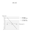
- FIG. 6B is a graph showing an output voltage before and after voltage compensation by the output control circuit over temperature.
- FIG. 6C is a graph showing a result of simulation in which a resistance of the ROI as the output specification temperature compensation element 330 in the form of a variable resistor as shown in FIG. 3A is trimmed using the temperature compensation circuit 600 in an effort to compensate the changes in the output voltage due to the temperature change and thereby the output voltage is maintained to be constant.
- the output specification calibrating apparatus enables to adjust non-linearity, offset, and gain of the capacitive pressure sensor, and thus it is feasible to satisfy various needs of customers for the specifications of the output of the capacitive pressure sensor by easily calibrating the output of the capacitive pressure sensor in a software manner.
Landscapes
- Physics & Mathematics (AREA)
- General Physics & Mathematics (AREA)
- Measuring Fluid Pressure (AREA)
Applications Claiming Priority (2)
| Application Number | Priority Date | Filing Date | Title |
|---|---|---|---|
| US13/737,189 US20140190237A1 (en) | 2013-01-09 | 2013-01-09 | Output specification calibrating apparatus for capacitive pressure sensor |
| KR1020130003543A KR101411625B1 (ko) | 2013-01-09 | 2013-01-11 | 용량성 압력센서의 출력사양 조정장치 |
Publications (2)
| Publication Number | Publication Date |
|---|---|
| EP2755005A2 true EP2755005A2 (de) | 2014-07-16 |
| EP2755005A3 EP2755005A3 (de) | 2017-01-25 |
Family
ID=49274556
Family Applications (1)
| Application Number | Title | Priority Date | Filing Date |
|---|---|---|---|
| EP13187300.2A Withdrawn EP2755005A3 (de) | 2013-01-09 | 2013-10-04 | Ausgangsspezifizierungskalibrierungsvorrichtung für kapazitiven Drucksensor |
Country Status (2)
| Country | Link |
|---|---|
| EP (1) | EP2755005A3 (de) |
| CN (1) | CN103913269A (de) |
Families Citing this family (7)
| Publication number | Priority date | Publication date | Assignee | Title |
|---|---|---|---|---|
| CN107076629B (zh) * | 2014-10-17 | 2020-06-16 | Vega格里沙贝两合公司 | 用于测定压力测量信号的方法以及用于该方法的压力测量装置 |
| JP6417246B2 (ja) * | 2015-03-17 | 2018-10-31 | アルプス電気株式会社 | 補正装置、補正方法、プログラム及び静電容量式圧力センサ |
| EP3203202B1 (de) * | 2016-02-08 | 2021-05-26 | Meggitt SA | Messschaltung |
| DE102018203419A1 (de) | 2018-03-07 | 2019-09-12 | Infineon Technologies Ag | Vorrichtung und verfahren zum kalibrieren einer druckerfassungseinrichtung |
| CN108956005B (zh) * | 2018-08-08 | 2024-03-22 | 陈德连 | 压力传感器 |
| CN113082686A (zh) * | 2021-04-30 | 2021-07-09 | 深圳益丰电子有限责任公司 | 一种多单元模拟压力传感器及电子投射靶 |
| DE102022105693B3 (de) * | 2022-03-10 | 2023-03-16 | Ifm Electronic Gmbh | Verfahren zum Betreiben einer Druckmesszelle eines kapazitiven Drucksensors |
Citations (1)
| Publication number | Priority date | Publication date | Assignee | Title |
|---|---|---|---|---|
| KR20010039983A (ko) | 1999-10-06 | 2001-05-15 | 사토 요시하루 | 용량성 압력센서 |
Family Cites Families (8)
| Publication number | Priority date | Publication date | Assignee | Title |
|---|---|---|---|---|
| US4392382A (en) * | 1981-03-09 | 1983-07-12 | Motorola Inc. | Linearized electronic capacitive pressure transducer |
| EP0245031B1 (de) * | 1986-05-05 | 1993-07-14 | Texas Instruments Incorporated | Messfühler hoher Präzision |
| US5135002A (en) * | 1989-08-29 | 1992-08-04 | Abbott Laboratories | Pressure transducer compensation system |
| US5241850A (en) * | 1991-11-01 | 1993-09-07 | Texas Instruments Incorporated | Sensor with programmable temperature compensation |
| US5329818A (en) * | 1992-05-28 | 1994-07-19 | Rosemount Inc. | Correction of a pressure indication in a pressure transducer due to variations of an environmental condition |
| US5770802A (en) * | 1997-04-16 | 1998-06-23 | Texas Instruments Incorporated | Sensor with improved capacitive to voltage converter integrated circuit |
| KR100453971B1 (ko) * | 2002-03-25 | 2004-10-20 | 전자부품연구원 | 적분형 용량-전압 변환장치 |
| US7216048B2 (en) * | 2004-12-30 | 2007-05-08 | Honeywell International Inc. | Calibrated pressure sensor |
-
2013
- 2013-10-04 EP EP13187300.2A patent/EP2755005A3/de not_active Withdrawn
- 2013-12-25 CN CN201310728515.9A patent/CN103913269A/zh active Pending
Patent Citations (1)
| Publication number | Priority date | Publication date | Assignee | Title |
|---|---|---|---|---|
| KR20010039983A (ko) | 1999-10-06 | 2001-05-15 | 사토 요시하루 | 용량성 압력센서 |
Also Published As
| Publication number | Publication date |
|---|---|
| CN103913269A (zh) | 2014-07-09 |
| EP2755005A3 (de) | 2017-01-25 |
Similar Documents
| Publication | Publication Date | Title |
|---|---|---|
| CN109687688B (zh) | 通过输入电压和输入电流感测来切换电压调节器的感测网络失配补偿 | |
| US9684018B2 (en) | Current sense circuit that operates over a wide range of currents | |
| US20140190237A1 (en) | Output specification calibrating apparatus for capacitive pressure sensor | |
| US20080122457A1 (en) | Capacitance difference detecting circuit | |
| EP2787331B1 (de) | Sensoranordnung für Lichterkennung und Temperaturerkennung und Verfahren für die Lichterkennung und Temperaturerkennung | |
| JP5900536B2 (ja) | センサ信号検出装置 | |
| JPS6057106B2 (ja) | オ−トゼロ積分器 | |
| TW200941174A (en) | Power management circuit and method of frequency compensation thereof | |
| KR20220027815A (ko) | 온도 측정 회로, 온도 및 광 측정 회로, 온도 측정 방법 및 온도 및 광 측정 방법 | |
| JP2000136966A (ja) | サ―モパイルセンサを用いた温度測定回路 | |
| EP3215858A2 (de) | Hochstrom-messschema mit verwendung von drain-source-spannung | |
| CN103913269A (zh) | 用于电容式压力传感器的输出规格校准设备 | |
| JP2018516408A (ja) | 低ドロップアウト電圧レギュレータ装置 | |
| US9310269B2 (en) | Analog front-end compensation | |
| KR101466857B1 (ko) | 안정도 보상 회로 및 이를 포함하는 dc-dc 컨버터 | |
| US20140015550A1 (en) | Detection circuit for capacitive sensor | |
| CN101128742B (zh) | 电流测量装置、测试装置、电流测量方法、及测试方法 | |
| TWI404316B (zh) | 具有改良的電流感測之直流至直流轉換器及相關之方法 | |
| US12176872B2 (en) | Current sensing circuit using temperature self-compensated trans-resistance amplifier | |
| US20070103174A1 (en) | Direct current test apparatus | |
| US9568518B2 (en) | Power measuring device with internal calibration of diode detectors | |
| JP4069158B1 (ja) | チャージアンプ、チャージアンプ装置、及び、バイアス電流補償方法 | |
| KR101446759B1 (ko) | 용량성 압력센서의 출력사양 조정장치 | |
| KR101355098B1 (ko) | 용량성 압력센서의 출력제어회로 | |
| KR101475710B1 (ko) | 용량성 압력센서 |
Legal Events
| Date | Code | Title | Description |
|---|---|---|---|
| PUAI | Public reference made under article 153(3) epc to a published international application that has entered the european phase |
Free format text: ORIGINAL CODE: 0009012 |
|
| 17P | Request for examination filed |
Effective date: 20131004 |
|
| AK | Designated contracting states |
Kind code of ref document: A2 Designated state(s): AL AT BE BG CH CY CZ DE DK EE ES FI FR GB GR HR HU IE IS IT LI LT LU LV MC MK MT NL NO PL PT RO RS SE SI SK SM TR |
|
| AX | Request for extension of the european patent |
Extension state: BA ME |
|
| PUAL | Search report despatched |
Free format text: ORIGINAL CODE: 0009013 |
|
| AK | Designated contracting states |
Kind code of ref document: A3 Designated state(s): AL AT BE BG CH CY CZ DE DK EE ES FI FR GB GR HR HU IE IS IT LI LT LU LV MC MK MT NL NO PL PT RO RS SE SI SK SM TR |
|
| AX | Request for extension of the european patent |
Extension state: BA ME |
|
| RIC1 | Information provided on ipc code assigned before grant |
Ipc: G01L 9/00 20060101AFI20161221BHEP Ipc: G01L 27/00 20060101ALI20161221BHEP Ipc: G01D 5/24 20060101ALI20161221BHEP Ipc: G01D 18/00 20060101ALI20161221BHEP Ipc: G01L 9/12 20060101ALI20161221BHEP |
|
| STAA | Information on the status of an ep patent application or granted ep patent |
Free format text: STATUS: THE APPLICATION IS DEEMED TO BE WITHDRAWN |
|
| 18D | Application deemed to be withdrawn |
Effective date: 20170726 |