EP2760258B1 - Ballast électronique - Google Patents
Ballast électronique Download PDFInfo
- Publication number
- EP2760258B1 EP2760258B1 EP12834014.8A EP12834014A EP2760258B1 EP 2760258 B1 EP2760258 B1 EP 2760258B1 EP 12834014 A EP12834014 A EP 12834014A EP 2760258 B1 EP2760258 B1 EP 2760258B1
- Authority
- EP
- European Patent Office
- Prior art keywords
- circuit
- switching element
- electrolytic capacitor
- electronic circuit
- pfc
- Prior art date
- Legal status (The legal status is an assumption and is not a legal conclusion. Google has not performed a legal analysis and makes no representation as to the accuracy of the status listed.)
- Active
Links
Images


Classifications
-
- H—ELECTRICITY
- H05—ELECTRIC TECHNIQUES NOT OTHERWISE PROVIDED FOR
- H05B—ELECTRIC HEATING; ELECTRIC LIGHT SOURCES NOT OTHERWISE PROVIDED FOR; CIRCUIT ARRANGEMENTS FOR ELECTRIC LIGHT SOURCES, IN GENERAL
- H05B47/00—Circuit arrangements for operating light sources in general, i.e. where the type of light source is not relevant
- H05B47/10—Controlling the light source
-
- H—ELECTRICITY
- H05—ELECTRIC TECHNIQUES NOT OTHERWISE PROVIDED FOR
- H05B—ELECTRIC HEATING; ELECTRIC LIGHT SOURCES NOT OTHERWISE PROVIDED FOR; CIRCUIT ARRANGEMENTS FOR ELECTRIC LIGHT SOURCES, IN GENERAL
- H05B41/00—Circuit arrangements or apparatus for igniting or operating discharge lamps
- H05B41/14—Circuit arrangements
- H05B41/26—Circuit arrangements in which the lamp is fed by power derived from DC by means of a converter, e.g. by high-voltage DC
- H05B41/28—Circuit arrangements in which the lamp is fed by power derived from DC by means of a converter, e.g. by high-voltage DC using static converters
-
- H—ELECTRICITY
- H05—ELECTRIC TECHNIQUES NOT OTHERWISE PROVIDED FOR
- H05B—ELECTRIC HEATING; ELECTRIC LIGHT SOURCES NOT OTHERWISE PROVIDED FOR; CIRCUIT ARRANGEMENTS FOR ELECTRIC LIGHT SOURCES, IN GENERAL
- H05B45/00—Circuit arrangements for operating light-emitting diodes [LED]
- H05B45/30—Driver circuits
- H05B45/355—Power factor correction [PFC]; Reactive power compensation
-
- H—ELECTRICITY
- H05—ELECTRIC TECHNIQUES NOT OTHERWISE PROVIDED FOR
- H05B—ELECTRIC HEATING; ELECTRIC LIGHT SOURCES NOT OTHERWISE PROVIDED FOR; CIRCUIT ARRANGEMENTS FOR ELECTRIC LIGHT SOURCES, IN GENERAL
- H05B45/00—Circuit arrangements for operating light-emitting diodes [LED]
- H05B45/30—Driver circuits
- H05B45/37—Converter circuits
- H05B45/3725—Switched mode power supply [SMPS]
- H05B45/39—Circuits containing inverter bridges
-
- Y—GENERAL TAGGING OF NEW TECHNOLOGICAL DEVELOPMENTS; GENERAL TAGGING OF CROSS-SECTIONAL TECHNOLOGIES SPANNING OVER SEVERAL SECTIONS OF THE IPC; TECHNICAL SUBJECTS COVERED BY FORMER USPC CROSS-REFERENCE ART COLLECTIONS [XRACs] AND DIGESTS
- Y02—TECHNOLOGIES OR APPLICATIONS FOR MITIGATION OR ADAPTATION AGAINST CLIMATE CHANGE
- Y02B—CLIMATE CHANGE MITIGATION TECHNOLOGIES RELATED TO BUILDINGS, e.g. HOUSING, HOUSE APPLIANCES OR RELATED END-USER APPLICATIONS
- Y02B20/00—Energy efficient lighting technologies, e.g. halogen lamps or gas discharge lamps
- Y02B20/30—Semiconductor lamps, e.g. solid state lamps [SSL] light emitting diodes [LED] or organic LED [OLED]
Definitions
- the present invention relates to electronic ballasts for gas discharge lamps, such as fluorescent lamps.
- Gas discharge lamps such as fluorescent lamps, generally include a ballast in their circuits, which in addition to generating the starting conditions of the lamp, is responsible for limiting the current to the load.
- the initial voltage or starting voltage is higher than the sustainability voltage; the ballast must be designed to handle various events, preserving the largest possible transfer of power to the load, with the most harmonious and appropriate treatment of the supply network and the lamp load.
- the impedance of the discharge lamp tends to an infinite value at shutdown conditions, but once the arc is generated when the gas is ionized inside the lamp, it changes of impedance until the lamp starts, wherein its impedance tends to zero, so that a current limiter element is incorporated between the network and the tube of the lamp, which is precisely the task performed by the ballast.
- Electronic ballasts typically include a rectifier in order to change the voltage of alternate current (AC) to a voltage of direct current (DC) and a filter circuit for filtering the DC voltage.
- the filter circuit usually comprises an energy storage capacitor.
- Electronic ballasts also often use booster circuits to amplify the magnitude of the DC voltage.
- ballasts that use means for power factor correction to reduce the total harmonic distortion of the ballast current input.
- These circuits usually include a switching inverter to convert the DC voltage in a high frequency AC voltage, and a resonant circuit which has a relatively high impedance for coupling the high frequency AC voltage to the electrodes of the discharge lamp.
- CCF current crest factor
- the current or voltage waveforms can be expressed as a fundamental and a series of harmonics. These harmonics have a certain frequency which is a multiple frequency of the fundamental frequency of the current or line voltage. Specifically, the distortion in AC waves has components which are integer multiples of the fundamental frequency. It is preferred that total harmonic distortion (THD) of the input current ballast is below 33.3 % to avoid overheating of the neutral thread in three phase power systems. In most cases, it is desirable that the ballast have a total harmonic distortion of the ballast's input current below 20%.
- TDD total harmonic distortion
- TDD total harmonic distortion
- CCF current crest factor
- U.S. patent 6,784,622 entitled “Single switch electronic dimming ballast,” discloses a ballast having an inverter circuit including a transformer with multiple secondary, one of which is used for repowering a high frequency level of the output of the storage capacitor in order to mitigate the valleys.
- the secondary windings are controlled by an electronic switch which at the same time shares the connection with an inverter circuit.
- the primary winding is controlled by a switch that belongs to a unit that has as a secondary winding that goes directly to the node 936 on the coil 42, capacitor 44 and the inverter.
- One of the transformers is connected through resistor 58 to the diode 54 to charge the capacitor 48.
- the capacitor 48 is charged positively via the resistor 58 to the diode 54 and its discharge is performed through the diode 52 to the circuit from the node located at the cathode of diode 840.
- the circuit configuration is inefficient during charge and discharge cycles of the capacitor as the capacitor is loaded on one wave half cycle, hence delivers voltage drops to zero at the half cycle where it is de-energized.
- the capacitor 48 allows decreasing part of the valley and rippling coming from the wave of the rectifier bridge, but the level of harmonic distortion (THD) rises significantly.
- the present invention discloses an electronic ballast for making a gas discharge lamp work which includes, in its preferred embodiment, (i) a rectifier circuit for converting an alternating current AC input voltage into a rectified voltage of direct current DC; (ii) a power factor correction (PFC) network which includes an electrolytic capacitor (or other energy storage device) that is loaded through a circuit conformed by an inductor, a diode and capacitor; and (iii) a switched inverter circuit that converts the rectified voltage of direct current to a high frequency alternating current, which has electrodes attached to the discharge lamps.
- PFC power factor correction
- the electronic circuit has a switching element that switches on the aforementioned elements making the PFC network consume power continuously following the supply voltage wave, while the electrolytic capacitor remains connected to the voltage of the rectifier bridge, through the inductor and diode, even if the inductor does not have energy stored.
- the switch Once the switch is closed, it does not affect the charge of the capacitor, because it is isolated by the diode which in this case is inversely polarized; when the switch is opened, the inductor releases the stored energy through the diode over the capacitor that was already charged to a voltage level close to the bridge voltage.
- the power factor correction (PFC) network controls the charge of the capacitor and inductor alternatively, resulting in a permanent and harmonic consumption of the network energy.
- the inverter is powered by the storage capacitor with a relatively constant voltage and noise free which allows the luminous load to be properly powered.
- the ballast further comprises a circuit for sensing the presence of lamps in the load circuit.
- the sensors are low-value resistors wherein a voltage drop is generated that identifies the values of the luminous load.
- the control is responsible for measuring the voltage levels at the low value resistors and, depending on the load, the duty cycle can be handled according to the system requirements. Consequently, the electronic ballast of the present invention can handle more than one gas discharge lamp with the maximum power transfer and greater efficiency.
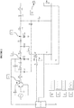
- the ballast (1) includes a rectifier circuit (2) connected to the network, usually an AC voltage at a frequency of 50 Hz or 60 Hz.
- a device Whenever it says that a device is connected, coupled, coupled in relation to current or that it may be connected to another device, it means that the device can be directly connected by a wire or as an alternative, get connected through another device such as, but not limited to, a resistor, diode, conductor device, and this connection may be serial or parallel.
- the rectifier circuit (2) converts the AC input voltage into a full wave rectified voltage.
- the rectifier circuit (2) is connected to a power factor correction (PFC) network (3).
- the power factor correction (PFC) network (3) generates a delay action on the load of one of the components of the circuit to allow smoothing the valleys of the rectified wave.
- the output terminals of the PFC network (3) are connected in turn to an inverter circuit (4).
- the inverter circuit (4) converts the DC voltage into a high frequency rectified AC voltage.
- the output terminals of the inverter circuit (4) provide essentially a high frequency sinusoidal voltage, and a voltage gain for starting the discharge lamps (5).
- the circuit (1) includes a series of sensors (6) over the current of luminous load (5) and sensors (8) on the PFC network (3), which provide information to the control circuit (7) of the load current to adjust the output power.
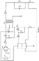
- FIG. 2 a schematic circuit of an embodiment of the present invention is shown with various PFC networks.
- the circuit is powered by an AC voltage source which is rectified by the rectifier bridge BR1.
- the rectified signal is shown with reference number 20, and it can be observed that it corresponds to a sine wave signal with very deep valleys.
- the first PFC stage defined by the capacitor C3 which is connected in parallel to an inductor L6 which is also connected in serial to diode D1, and to an electrolytic storage and filter capacitor C4.
- the electronic circuit of this embodiment is switching by a switching element Ql, which allows control over the network PFC.
- the values and references of the elements in the figures are merely illustrative. They can be modified to optimize various design parameters.
- the network that generates a PFC delay action over the load may be comprised of an inductor L2 and diode D1 connected between the electrolytic capacitor C4 and the switching element Q1 through the diode D2, and in the same way generate a delay action over the load or over the next PFC stage.
- a first oscillation phase where the switching element Q1 is open, there is a current flow from the positive node of the rectifier bridge to the first PFC stage (capacitor C3, inductor L6, diode D1 and the electrolytic capacitor C4).
- the switching element Q1 when the switching element Q1 is closed, the current flows from the positive node of the rectifier bridge BR1 through the inductor L2, diode D2 and switching element Q1 to ground.
- the switch element Q1 may be a metal-oxide-semiconductor field-effect transistor (MOSFET), but may also be a bipolar junction transistor (BJT), or an insulated-gate bipolar transistor (IGBT) or other common controllably conductive devices.
- MOSFET metal-oxide-semiconductor field-effect transistor
- BJT bipolar junction transistor
- IGBT insulated-gate bipolar transistor
- the configuration of capacitor C3 and inductor L6 generates a delay over the action of the electrolytic capacitor C4 compared to the moment it closes and opens the switching element Ql, since the capacitor C3 (in the electric field) and the inductor L6 (in the magnetic field) alternatively store energy for a short period of time.
- This configuration of electronic elements tends to offset the discharge action of the electrolytic capacitor C4 in time compared to the initial charge action of the same capacitor C4. Thanks to the offset generated by reactive elements L6, C3 and diode D1, in their respective fields (magnetic and electric), it has provided a continuous power source over the electrolytic capacitor C4 at all times.
- the L6 and C3 elements introduce a delay or phase difference in the action of switch Q1 for the load over C4, which is one of the essential elements in the filter to prevent rippling.
- inductor L2 discharges the energy stored through D1 over C4 leaving the circuit permanently connected.
- the delay allows the circuit to provide power stability for the moments when the load requires electric power; in particular inductor L2 and rectifier BR1 provide load capacity to capacitor C4 and thus to supply the requirements of the circuit.
- This generates greater stability to the output voltage of the discharge lamp; provides lower fluctuations, and provides minor harmonics, all of this with the action of a single switching element Q1.
- This effect can be reflected in the output node of the PFC circuit shown with reference number 21, where a smoother and filtered signal is shown, compared to the output signal in the positive node of BR1 shown with the reference number 20.
- the circuit of the present invention allows the handling of multiple PFC network stages with their respective inverter circuits and only one switch Q1 at the same time, thanks to the delays provided by the PFC networks.
- additional L-C branches may be placed with different discharge lamps with different power load in a serial or parallel connection, dimensioning the switching element Q to the requirements of the new equivalent network.
- RC values should be calculated so that the harmonic response is the lowest, and the power factor is the highest.
- the sizing of new stages requires the setting of electrolytic capacitor C4 to a lower value and the use of a second electrolytic capacitor C7 (following Figure 2 ) in a second stage with a higher value, looking for a lower level of harmonic distortion and power factor close to 1.
- the embodiment illustrated in Figure 2 has two PFC stages.
- the first stage is connected in series to the second stage through the joining point with the storage and filtering electrolytic capacitor C4.
- the first stage provides a pre-filtered voltage of the correction circuit (Boost type circuit) conformed by inductors L4, L5, diode D5 and capacitor C7.
- the inductor L5 generates a new delay in the action over the anode of diode D5, offsetting the response compared to the previous stage.
- This configuration allows, with a single switching element, to handle two different stages: i) the PFC network, and ii) the inverter circuits. Also, as a skilled person can observe, the switching element may act on additional stages that contribute to filtering, power factor correction and improved harmonic response.
- Boost-type circuit When the present invention states that a part of the circuit is a Boost-type circuit, it should be understood that this corresponds to a rectifier bridge that goes through an inductor and is switched by a semiconductor switch.
- the switch Q1 In the second stage of the circuit shown in Figure 2 , when the switch Q1 is closed, the current flow occurs through the inductor L4, the switch Q1 through the inductor L5, which enables the charge of the electrolytic capacitor C7. Once the switch Q1 opens, the remaining current in L4 provides the remaining energy in its magnetic field passing it to the inverter circuit.
- the configuration of the second PFC stage provides a delay in the action of the electrolytic capacitor C7 compared with the time the switching element Q1 closes and opens.
- the circuit never loses power and instead, the circuit is permanently connected under DC conditions. That is, in the switching of the switching element Q1 the circuit will always be electrically supported by: i) the rectifier circuit when the switch has not yet entered into oscillation, and ii) due to the L-C configuration of the PFC network at the time in which the switch after closing the switch, it is then opened.
- the capacitor C4 is preloaded from the full wave bridge rectifier BR1 through inductor L6 and diode D1.
- the electrolytic capacitor C4 receives a DC voltage value corresponding to the value of the voltage at the positive node of the full wave rectifier BR1.
- the capacitor C4 when the switch Q1 is closed, the capacitor C4 has a load that is not affected by the closing of switch Ql, thanks to the diode D1. And at the time the switch Q1 is opened, the electrolytic capacitor C4 is still receiving the electric support of elements L6-C3 connected in series therewith. This allows the circuit to reduce the level of harmonics and provide higher power.
- the last stage connected to the output of the second PFC network consists in a capacitor C2 and an inductor L1 in series that provide a high frequency voltage to operate one or more discharge lamps.
- R7 represents the discharge lamp and R3 represents a sensing resistor that will provide load information to the control circuit as will be described later.
- the high frequency voltage can be displayed on the discharge lamp R7 represented by reference number 23.
- the circuit of the present invention provides the advantage that, in the event that the load or the discharge lamp is removed, there would not consumption since the circuit only requires the connection of the two terminals of the lamp, and not the four terminals as the prior art does. If it were to break the filament of the discharge lamp, the lamp does not turn off, but will be kept on, because the filaments are not a required passage in the circuit.
- This also provides the possibility of increasing the duty cycle by changing the output voltage of the load lifting it during boot time and after a while the voltage is lowered to the maintenance voltage, by modifying the duty cycle or frequency signal or a combination of both.
- the circuit of the present invention provides a conventional control module for monitoring the presence of lamps in the system, detecting the load impedance and thus provides the voltage required for booting and maintenance.
- the control module can take the decision based on a program to increase the duty cycle with a specified or programmed time to ensure the booting of the discharge lamp. Once the control module detects the booting thanks to the current sensor, it adjusts the duty cycle and/or frequency to the condition of maintenance complying with the maximum power transfer to the lamp.
- the control module can be configured in a mode called "displacement modulation," which is nothing but the variation of pulse width and frequency.
- the control module can be any type of electronic controller with programming features, analog and digital inputs and outputs.
- the control modules can be comprised by integrated circuits called PSoC levels 3 or 5, or SmartFusion integrated circuits.
- This module based on the current feedback signal of the load, the current through the switch Q1 and the input voltage over the electrolytic capacitor C4, takes a decision as to whether the lamp has started or not.
- the control module may vary the duty cycle from 22% to 66% to boot the lamp and can even vary the frequency of the oscillator that powers the gate of the switch Q1, to contribute the boot.
- the maintenance frequency is approximately 55 kHz and the duty cycle between 22% and 33% for the maintenance condition. The change in frequency is done so that the output voltage over the discharge lamp R7 goes to the maintenance level, or auto-tuning for different lamp references.
- control module can increase the duty cycle, and also change the frequency to increase the output voltage over the load and turn it on.
- the module allows the booting of any type of lamp depending on the maintenance load voltage detecting the change in impedance, so that the duty cycle can be modified, and the output voltage on the load voltage support can be increased or decreased.
- the control module is able to determine what kind of load is present, when comparing within its operating parameters, if the current through the sensing resistor R4 corresponds to a set voltage range.
- the control module analyzes the load current through the sensor element R4, and the voltage across the electrolytic capacitor C4 and based on these feedback values determine the output power by adjusting the voltage and changing the duty cycle, trying not to deform the current waveform in order to not to increase the harmonics of the system. If the control module cannot read the presence of load for a while, the module increases the duty cycle, and can even change the frequency to be sufficient to generate the boot.
- the sensor element R4, that have just sensed, sends the booting signal due to an increase in current and the control module makes the necessary adjustments in duty cycle and frequency for the system to operate properly in sustaining or maintenance.
- control module compares the settings in the duty cycle and frequency generated for the booting of the lamp with information contained within the module and determines what type of lamp is connected to the circuit (for example, the circuit can determine if a lamp corresponds to the group T8 of 32 watts, or a T8 lamp of 17 watts, or a lamp F40 T 12 of 40 watts, etc.), making the necessary adjustments to optimize the values of voltage, harmonic distortion (THD) and power factor for each type of load connected.
- TDD harmonic distortion
- the inductor TR1 is present for amplification purposes and circuit protection (flyback type).
- the electrolytic capacitor C4 is isolated from the positive node of the rectifier bridge BR1, allowing that when the switching element Q1 is closed, a way to the positive node of the bridge is generated through L2, D2, switch Q1 and ground.
- the electrolytic capacitor C4 is charged through D1 and discharged through the circuit, disabling the discharge through diode D1 by means of the oppositely polarized.
- the capacitor C3 represents an element for signal filtering purposes on the load, but is optional and may or may not go in parallel with the load.
- the ballast circuit detects the state (ON/OFF) of the lamp R7 which is connected in series through R5. If any current that represents the lamp ignition is detected, the circuit through R5 and the control unit, increases rapidly the duty cycle for a short period in order for the lamp to be energized and change the impedance characteristics making the current to be increased and be detected by R5 to bring the signal to the control unit. Then, the control module lowers the duty cycle to a level that allows the voltage decrease to the point of maintenance.
- resistors R6 and R8 are low value resistors that generate a low drop voltage value to sense current on lamp R7. They read the variations that may occur in the load voltage.
- the positive node of the rectifier bridge is connected to the drain of the switch.
- Diode D3 is inversely connected in such a way that prevents the flow of current through the inverter bridge.
- the inverter has the switch Q1 as the switch element which is isolated by diode D2 from the rest of the circuit.
- This configuration is a class E inverter that has a capacitor C6 in parallel with the load R7, which by its setting filters eddy currents and improves the response of the circuit.
Landscapes
- Circuit Arrangements For Discharge Lamps (AREA)
- Rectifiers (AREA)
- Inverter Devices (AREA)
Claims (15)
- Un circuit électronique pour le fonctionnement de lampes à décharge (R7), comprenant :a- un pont redresseur (BR1) connecté à une source d'alimentation en courant alternatif ;b- un réseau (3) de correction de facteur de puissance (PFC) connecté à la sortie du pont redresseur (BR1), qui contient un condensateur électrolytique de stockage et de filtrage (C4) qui est chargé par un premier étage PFC défini par un condensateur (C3) connecté en parallèle à une inductance (L6) également en série avec une diode (D1), le réseau (3) de correction de facteur de puissance (PFC) générant une action de retard sur la charge du condensateur électrolytique de stockage et de filtrage (C4) ;c- un circuit inverseur (4) connecté à la sortie du réseau PFC (3), contenant un élément de commutation (Q1) ;d- un module de commande qui reçoit et traite les signaux de courant provenant du courant de la lampe à décharge (R7) et la tension sur le condensateur électrolytique de stockage et de filtrage (C4), afin de commander l'élément de commutation (Q1) ;dans lequel
le réseau PFC (3) et le circuit inverseur (4) partageant l'élément de commutation (Q1) ;
le condensateur électrolytique de stockage et de filtrage (C4) est connecté de façon permanente au pont redresseur (BR1) dans des conditions de courant continu, et
dans l'intervalle de temps pendant lequel l'élément de commutation (Q1) est fermé, le condensateur électrolytique de stockage et de filtrage (C4) est préchargé depuis le pont redresseur pleine onde (BR1) par l'inductance (L6) et le condensateur (C3) du premier étage PFC, et
au moment où l'élément de commutation (Q1) est ouvert, le condensateur électrolytique de stockage et de filtrage (C4) reçoit toujours le support électrique de l'inductance (L6) et la diode (D1) du premier étage PFC. - Le circuit électronique selon la revendication 1, dans lequel le circuit comporte une pluralité de réseaux PFC partageant le même élément de commutation (Q1).
- Le circuit électronique selon la revendication 1, dans lequel le circuit comporte une pluralité d'inverseurs qui partagent le même élément de commutation (Q1).
- Le circuit électronique selon la revendication 1, dans lequel le réseau PFC (3) comprend une inductance (L6) et une diode (D1) reliées entre le condensateur électrolytique de stockage et de filtrage (C4) et, par l'intermédiaire d'une autre diode (D2), à l'élément de commutation (Q1).
- Le circuit électronique selon la revendication 4, dans lequel le réseau PFC (3) comprend en outre un circuit de décalage.
- Le circuit électronique selon la revendication 4, dans lequel le circuit de décalage est un condensateur électrolytique (C7).
- Le circuit électronique selon la revendication 1, dans lequel la lampe à décharge (R7) est en série avec la sortie du circuit inverseur (4).
- Le circuit électronique selon la revendication 1, dans lequel le circuit inverseur (4) est un circuit inverseur de type classe E flyback ou résonant.
- Le circuit électronique selon la revendication 1, dans lequel l'élément de commutation (Q1) est un transistor.
- Le circuit électronique selon la revendication 1, dans lequel le circuit inverseur (4) est un onduleur résonnant.
- Le circuit électronique selon la revendication 1, dans lequel l'élément de commutation (Q1), la lampe à décharge (R7) et le condensateur électrolytique de stockage et de filtrage (C4) sont connectés à des résistances de faible valeur (R3, R4) qui fonctionnent comme des détecteurs de courant.
- Le circuit électronique selon la revendication 1, dans lequel le pont redresseur (BR1) est isolé du condensateur électrolytique de stockage et de filtrage (C4) par l'intermédiaire d'une diode (D1).
- Le circuit électronique selon la revendication 1, dans lequel l'effet de commutation de l'élément de commutation (Q1) augmente la charge de tension du condensateur électrolytique de stockage et de filtrage (C4).
- Le circuit électronique selon la revendication 1, dans lequel le condensateur électrolytique de stockage et de filtrage (C4) reçoit toujours une tension positive lorsque l'élément de commutation (Q1) est ouvert.
- Le circuit électronique selon la revendication 1, dans lequel les lampes à décharge (R7) sont des lampes fluorescentes.
Applications Claiming Priority (2)
| Application Number | Priority Date | Filing Date | Title |
|---|---|---|---|
| CO11124965A CO6530147A1 (es) | 2011-09-23 | 2011-09-23 | Balaso electrónico |
| PCT/IB2012/055045 WO2013042092A2 (fr) | 2011-09-23 | 2012-09-22 | Ballast électronique |
Publications (3)
| Publication Number | Publication Date |
|---|---|
| EP2760258A2 EP2760258A2 (fr) | 2014-07-30 |
| EP2760258A4 EP2760258A4 (fr) | 2015-12-16 |
| EP2760258B1 true EP2760258B1 (fr) | 2018-03-07 |
Family
ID=47069084
Family Applications (1)
| Application Number | Title | Priority Date | Filing Date |
|---|---|---|---|
| EP12834014.8A Active EP2760258B1 (fr) | 2011-09-23 | 2012-09-22 | Ballast électronique |
Country Status (6)
| Country | Link |
|---|---|
| US (1) | US8981660B2 (fr) |
| EP (1) | EP2760258B1 (fr) |
| JP (1) | JP6262135B2 (fr) |
| CN (1) | CN104041192B (fr) |
| CO (1) | CO6530147A1 (fr) |
| WO (1) | WO2013042092A2 (fr) |
Family Cites Families (28)
| Publication number | Priority date | Publication date | Assignee | Title |
|---|---|---|---|---|
| JP3128982B2 (ja) * | 1992-09-17 | 2001-01-29 | 富士通株式会社 | Dc−dcコンバータ |
| US5381076A (en) * | 1993-10-18 | 1995-01-10 | General Electric Company | Metal halide electronic ballast |
| US5416388A (en) * | 1993-12-09 | 1995-05-16 | Motorola Lighting, Inc. | Electronic ballast with two transistors and two transformers |
| JPH09251896A (ja) * | 1996-03-15 | 1997-09-22 | Toshiba Lighting & Technol Corp | 放電灯点灯装置及び照明装置 |
| US6222322B1 (en) * | 1997-09-08 | 2001-04-24 | Q Technology Incorporated | Ballast with lamp abnormal sensor and method therefor |
| IL138493A0 (en) * | 2000-09-15 | 2001-10-31 | Lightech Electronics Ind Ltd | Electronic ballast for high-intensity discharge lamps |
| US6784622B2 (en) | 2001-12-05 | 2004-08-31 | Lutron Electronics Company, Inc. | Single switch electronic dimming ballast |
| US6686705B2 (en) * | 2002-01-25 | 2004-02-03 | General Electric Company | Ballast circuit with multiple inverters and dimming controller |
| US6936973B2 (en) * | 2002-05-31 | 2005-08-30 | Jorge M. Parra, Sr. | Self-oscillating constant-current gas discharge device lamp driver and method |
| KR100510110B1 (ko) * | 2002-08-20 | 2005-08-24 | 라이트전자 주식회사 | 티파이브 형광 램프용 전자식 안정기 |
| DE10242332A1 (de) * | 2002-09-12 | 2004-03-25 | Tridonicatco Gmbh & Co. Kg | Elektronisches Vorschaltgerät mit Ladungspumpe zur aktiven Leistungsfaktorkorrektur |
| DE10303276A1 (de) * | 2003-01-28 | 2004-07-29 | Patent-Treuhand-Gesellschaft für elektrische Glühlampen mbH | Schaltungsanordnung und Verfahren zum Start und Betrieb von Entladungslampen |
| JP4144417B2 (ja) * | 2003-04-22 | 2008-09-03 | 松下電工株式会社 | 放電灯点灯装置及び照明器具 |
| US7038396B2 (en) * | 2003-10-22 | 2006-05-02 | Amf Technology, Inc. | Electronic high intensity discharge lamp driver |
| US7187136B2 (en) * | 2004-10-25 | 2007-03-06 | Osram Sylvania, Inc. | Method and circuit for regulating power in a high intensity discharge lamp |
| US7432661B2 (en) * | 2005-05-02 | 2008-10-07 | Lutron Electronics Co., Inc. | Electronic ballast having a flyback cat-ear power supply |
| WO2006117809A1 (fr) * | 2005-05-04 | 2006-11-09 | Stmicroelectronics S.R.L. | Systeme de commande pour lampe a decharge |
| CN2907170Y (zh) * | 2006-05-16 | 2007-05-30 | 彭俊忠 | 节电稳压镇流装置 |
| JP2007288855A (ja) * | 2006-04-13 | 2007-11-01 | Sanken Electric Co Ltd | スイッチング電源装置 |
| US20100194287A1 (en) * | 2007-02-01 | 2010-08-05 | Roberto Vivero-Flores | Electronic ballast for a high intensity discharge lamp |
| US7528554B2 (en) * | 2007-05-11 | 2009-05-05 | Lutron Electronics Co., Inc. | Electronic ballast having a boost converter with an improved range of output power |
| GB2452261A (en) * | 2007-08-29 | 2009-03-04 | Cambridge Semiconductor Ltd | Discharge lamp controller with SEPIC and push-pull stage |
| EP2345310A4 (fr) | 2008-06-13 | 2013-01-16 | Univ Kingston | Ballast électronique à étage unique à gradation à facteur de puissance élevé |
| WO2010055528A2 (fr) * | 2008-11-14 | 2010-05-20 | Kartik Prafull Bakeri | Montage de circuit de protection économique et durable avec faibles harmoniques |
| DE102009009915A1 (de) * | 2009-01-09 | 2010-07-15 | Tridonicatco Gmbh & Co. Kg | Verfahren, Betriebsgerät und Beleuchtungssystem |
| CN201509352U (zh) * | 2009-10-23 | 2010-06-16 | 山东华琪电器有限公司 | 一种emc电路 |
| US8410718B2 (en) * | 2010-05-27 | 2013-04-02 | Osram Sylvania Inc. | Dimmer conduction angle detection circuit and system incorporating the same |
| US8339056B1 (en) * | 2010-06-17 | 2012-12-25 | Universal Lighting Technologies, Inc. | Lamp ballast with protection circuit for input arcing and line interruption |
-
2011
- 2011-09-23 CO CO11124965A patent/CO6530147A1/es unknown
-
2012
- 2012-09-22 EP EP12834014.8A patent/EP2760258B1/fr active Active
- 2012-09-22 JP JP2014531365A patent/JP6262135B2/ja active Active
- 2012-09-22 CN CN201280057660.2A patent/CN104041192B/zh active Active
- 2012-09-22 WO PCT/IB2012/055045 patent/WO2013042092A2/fr not_active Ceased
- 2012-09-22 US US14/346,483 patent/US8981660B2/en active Active
Non-Patent Citations (1)
| Title |
|---|
| None * |
Also Published As
| Publication number | Publication date |
|---|---|
| EP2760258A2 (fr) | 2014-07-30 |
| JP2014526789A (ja) | 2014-10-06 |
| US20140232286A1 (en) | 2014-08-21 |
| WO2013042092A3 (fr) | 2013-06-20 |
| CO6530147A1 (es) | 2012-09-28 |
| EP2760258A4 (fr) | 2015-12-16 |
| CN104041192A (zh) | 2014-09-10 |
| CN104041192B (zh) | 2016-08-24 |
| US8981660B2 (en) | 2015-03-17 |
| WO2013042092A2 (fr) | 2013-03-28 |
| JP6262135B2 (ja) | 2018-01-17 |
Similar Documents
| Publication | Publication Date | Title |
|---|---|---|
| US6316883B1 (en) | Power-factor correction circuit of electronic ballast for fluorescent lamps | |
| US5583402A (en) | Symmetry control circuit and method | |
| US20090295300A1 (en) | Methods and apparatus for a dimmable ballast for use with led based light sources | |
| EP0683966A1 (fr) | Ballast electronique a deux transistors et deux transformateurs | |
| JP2003520407A (ja) | 多ランプ動作用の電力帰還力率修正方式 | |
| CA2718423A1 (fr) | Ballast electronique pour lampes a decharge a haute intensite | |
| WO2012151712A1 (fr) | Circuit amélioré d'allumage programmé pour ballast | |
| JPH11507176A (ja) | 力率補正機能を有する単一スイッチ・バラスト | |
| JPH0329298A (ja) | ガス放電ランプ用安定回路 | |
| CN104396128B (zh) | 功率因数校正电路、用于照明用具的操作装置和用于控制功率因数校正电路的方法 | |
| JP2009518835A (ja) | 少なくとも1つのledを作動するための回路装置及びその作動方法 | |
| US6933681B2 (en) | Circuit arrangement and method for starting and operating discharge lamps | |
| US20100188021A1 (en) | Electronic ballast and method for operating at least one discharge lamp | |
| EP4049516B1 (fr) | Pilote del pour systèmes d'éclairage à del de remplacement d'une lampe de décharge haute intensité | |
| CN101606440A (zh) | 用于在正常操作和调光期间具有高效率的高功率因数镇流器的方法和设备 | |
| US8981660B2 (en) | Electronic ballast | |
| US7145293B2 (en) | Electronic ballast having resonance excitation for generating a transfer voltage | |
| JP2004527896A (ja) | 高効率高力率電子安定器 | |
| US6005353A (en) | Commutator for a discharge lamp having mutually coupled inductors | |
| JP2007524212A (ja) | 点灯回路及びその動作方法、駆動回路 | |
| CN203708126U (zh) | 供电电路、加热装置的控制电路和加热装置 | |
| CN103746576A (zh) | 供电电路、加热装置的控制电路和加热装置 | |
| CN113455106B (zh) | 用于替换高强度放电灯的led照明单元的led驱动器 | |
| US11277891B2 (en) | Control method and control circuit of electronic ballast of gas discharge lamp (HID) | |
| Lopes et al. | Automatic lamp detection technique for fluorescent lamps electronic ballasts |
Legal Events
| Date | Code | Title | Description |
|---|---|---|---|
| PUAI | Public reference made under article 153(3) epc to a published international application that has entered the european phase |
Free format text: ORIGINAL CODE: 0009012 |
|
| 17P | Request for examination filed |
Effective date: 20140421 |
|
| AK | Designated contracting states |
Kind code of ref document: A2 Designated state(s): AL AT BE BG CH CY CZ DE DK EE ES FI FR GB GR HR HU IE IS IT LI LT LU LV MC MK MT NL NO PL PT RO RS SE SI SK SM TR |
|
| DAX | Request for extension of the european patent (deleted) | ||
| A4 | Supplementary search report drawn up and despatched |
Effective date: 20151116 |
|
| RIC1 | Information provided on ipc code assigned before grant |
Ipc: H05B 37/02 20060101ALI20151110BHEP Ipc: H05B 41/28 20060101AFI20151110BHEP |
|
| 17Q | First examination report despatched |
Effective date: 20161205 |
|
| GRAP | Despatch of communication of intention to grant a patent |
Free format text: ORIGINAL CODE: EPIDOSNIGR1 |
|
| INTG | Intention to grant announced |
Effective date: 20170811 |
|
| GRAJ | Information related to disapproval of communication of intention to grant by the applicant or resumption of examination proceedings by the epo deleted |
Free format text: ORIGINAL CODE: EPIDOSDIGR1 |
|
| INTC | Intention to grant announced (deleted) | ||
| GRAR | Information related to intention to grant a patent recorded |
Free format text: ORIGINAL CODE: EPIDOSNIGR71 |
|
| GRAS | Grant fee paid |
Free format text: ORIGINAL CODE: EPIDOSNIGR3 |
|
| GRAA | (expected) grant |
Free format text: ORIGINAL CODE: 0009210 |
|
| AK | Designated contracting states |
Kind code of ref document: B1 Designated state(s): AL AT BE BG CH CY CZ DE DK EE ES FI FR GB GR HR HU IE IS IT LI LT LU LV MC MK MT NL NO PL PT RO RS SE SI SK SM TR |
|
| INTG | Intention to grant announced |
Effective date: 20180130 |
|
| REG | Reference to a national code |
Ref country code: GB Ref legal event code: FG4D |
|
| REG | Reference to a national code |
Ref country code: CH Ref legal event code: EP Ref country code: AT Ref legal event code: REF Ref document number: 977916 Country of ref document: AT Kind code of ref document: T Effective date: 20180315 |
|
| REG | Reference to a national code |
Ref country code: IE Ref legal event code: FG4D |
|
| REG | Reference to a national code |
Ref country code: DE Ref legal event code: R096 Ref document number: 602012043839 Country of ref document: DE |
|
| REG | Reference to a national code |
Ref country code: NL Ref legal event code: FP |
|
| REG | Reference to a national code |
Ref country code: LT Ref legal event code: MG4D |
|
| PG25 | Lapsed in a contracting state [announced via postgrant information from national office to epo] |
Ref country code: ES Free format text: LAPSE BECAUSE OF FAILURE TO SUBMIT A TRANSLATION OF THE DESCRIPTION OR TO PAY THE FEE WITHIN THE PRESCRIBED TIME-LIMIT Effective date: 20180307 Ref country code: LT Free format text: LAPSE BECAUSE OF FAILURE TO SUBMIT A TRANSLATION OF THE DESCRIPTION OR TO PAY THE FEE WITHIN THE PRESCRIBED TIME-LIMIT Effective date: 20180307 Ref country code: CY Free format text: LAPSE BECAUSE OF FAILURE TO SUBMIT A TRANSLATION OF THE DESCRIPTION OR TO PAY THE FEE WITHIN THE PRESCRIBED TIME-LIMIT Effective date: 20180307 Ref country code: NO Free format text: LAPSE BECAUSE OF FAILURE TO SUBMIT A TRANSLATION OF THE DESCRIPTION OR TO PAY THE FEE WITHIN THE PRESCRIBED TIME-LIMIT Effective date: 20180607 Ref country code: FI Free format text: LAPSE BECAUSE OF FAILURE TO SUBMIT A TRANSLATION OF THE DESCRIPTION OR TO PAY THE FEE WITHIN THE PRESCRIBED TIME-LIMIT Effective date: 20180307 Ref country code: HR Free format text: LAPSE BECAUSE OF FAILURE TO SUBMIT A TRANSLATION OF THE DESCRIPTION OR TO PAY THE FEE WITHIN THE PRESCRIBED TIME-LIMIT Effective date: 20180307 |
|
| REG | Reference to a national code |
Ref country code: AT Ref legal event code: MK05 Ref document number: 977916 Country of ref document: AT Kind code of ref document: T Effective date: 20180307 |
|
| PG25 | Lapsed in a contracting state [announced via postgrant information from national office to epo] |
Ref country code: GR Free format text: LAPSE BECAUSE OF FAILURE TO SUBMIT A TRANSLATION OF THE DESCRIPTION OR TO PAY THE FEE WITHIN THE PRESCRIBED TIME-LIMIT Effective date: 20180608 Ref country code: RS Free format text: LAPSE BECAUSE OF FAILURE TO SUBMIT A TRANSLATION OF THE DESCRIPTION OR TO PAY THE FEE WITHIN THE PRESCRIBED TIME-LIMIT Effective date: 20180307 Ref country code: BG Free format text: LAPSE BECAUSE OF FAILURE TO SUBMIT A TRANSLATION OF THE DESCRIPTION OR TO PAY THE FEE WITHIN THE PRESCRIBED TIME-LIMIT Effective date: 20180607 Ref country code: LV Free format text: LAPSE BECAUSE OF FAILURE TO SUBMIT A TRANSLATION OF THE DESCRIPTION OR TO PAY THE FEE WITHIN THE PRESCRIBED TIME-LIMIT Effective date: 20180307 Ref country code: SE Free format text: LAPSE BECAUSE OF FAILURE TO SUBMIT A TRANSLATION OF THE DESCRIPTION OR TO PAY THE FEE WITHIN THE PRESCRIBED TIME-LIMIT Effective date: 20180307 |
|
| REG | Reference to a national code |
Ref country code: FR Ref legal event code: PLFP Year of fee payment: 7 |
|
| PG25 | Lapsed in a contracting state [announced via postgrant information from national office to epo] |
Ref country code: IT Free format text: LAPSE BECAUSE OF FAILURE TO SUBMIT A TRANSLATION OF THE DESCRIPTION OR TO PAY THE FEE WITHIN THE PRESCRIBED TIME-LIMIT Effective date: 20180307 Ref country code: RO Free format text: LAPSE BECAUSE OF FAILURE TO SUBMIT A TRANSLATION OF THE DESCRIPTION OR TO PAY THE FEE WITHIN THE PRESCRIBED TIME-LIMIT Effective date: 20180307 Ref country code: PL Free format text: LAPSE BECAUSE OF FAILURE TO SUBMIT A TRANSLATION OF THE DESCRIPTION OR TO PAY THE FEE WITHIN THE PRESCRIBED TIME-LIMIT Effective date: 20180307 Ref country code: AL Free format text: LAPSE BECAUSE OF FAILURE TO SUBMIT A TRANSLATION OF THE DESCRIPTION OR TO PAY THE FEE WITHIN THE PRESCRIBED TIME-LIMIT Effective date: 20180307 Ref country code: EE Free format text: LAPSE BECAUSE OF FAILURE TO SUBMIT A TRANSLATION OF THE DESCRIPTION OR TO PAY THE FEE WITHIN THE PRESCRIBED TIME-LIMIT Effective date: 20180307 |
|
| PG25 | Lapsed in a contracting state [announced via postgrant information from national office to epo] |
Ref country code: SM Free format text: LAPSE BECAUSE OF FAILURE TO SUBMIT A TRANSLATION OF THE DESCRIPTION OR TO PAY THE FEE WITHIN THE PRESCRIBED TIME-LIMIT Effective date: 20180307 Ref country code: AT Free format text: LAPSE BECAUSE OF FAILURE TO SUBMIT A TRANSLATION OF THE DESCRIPTION OR TO PAY THE FEE WITHIN THE PRESCRIBED TIME-LIMIT Effective date: 20180307 Ref country code: CZ Free format text: LAPSE BECAUSE OF FAILURE TO SUBMIT A TRANSLATION OF THE DESCRIPTION OR TO PAY THE FEE WITHIN THE PRESCRIBED TIME-LIMIT Effective date: 20180307 Ref country code: SK Free format text: LAPSE BECAUSE OF FAILURE TO SUBMIT A TRANSLATION OF THE DESCRIPTION OR TO PAY THE FEE WITHIN THE PRESCRIBED TIME-LIMIT Effective date: 20180307 |
|
| REG | Reference to a national code |
Ref country code: DE Ref legal event code: R097 Ref document number: 602012043839 Country of ref document: DE |
|
| PG25 | Lapsed in a contracting state [announced via postgrant information from national office to epo] |
Ref country code: PT Free format text: LAPSE BECAUSE OF FAILURE TO SUBMIT A TRANSLATION OF THE DESCRIPTION OR TO PAY THE FEE WITHIN THE PRESCRIBED TIME-LIMIT Effective date: 20180709 |
|
| PLBE | No opposition filed within time limit |
Free format text: ORIGINAL CODE: 0009261 |
|
| STAA | Information on the status of an ep patent application or granted ep patent |
Free format text: STATUS: NO OPPOSITION FILED WITHIN TIME LIMIT |
|
| PG25 | Lapsed in a contracting state [announced via postgrant information from national office to epo] |
Ref country code: DK Free format text: LAPSE BECAUSE OF FAILURE TO SUBMIT A TRANSLATION OF THE DESCRIPTION OR TO PAY THE FEE WITHIN THE PRESCRIBED TIME-LIMIT Effective date: 20180307 |
|
| 26N | No opposition filed |
Effective date: 20181210 |
|
| PG25 | Lapsed in a contracting state [announced via postgrant information from national office to epo] |
Ref country code: SI Free format text: LAPSE BECAUSE OF FAILURE TO SUBMIT A TRANSLATION OF THE DESCRIPTION OR TO PAY THE FEE WITHIN THE PRESCRIBED TIME-LIMIT Effective date: 20180307 |
|
| PG25 | Lapsed in a contracting state [announced via postgrant information from national office to epo] |
Ref country code: MC Free format text: LAPSE BECAUSE OF FAILURE TO SUBMIT A TRANSLATION OF THE DESCRIPTION OR TO PAY THE FEE WITHIN THE PRESCRIBED TIME-LIMIT Effective date: 20180307 |
|
| REG | Reference to a national code |
Ref country code: CH Ref legal event code: PL |
|
| REG | Reference to a national code |
Ref country code: BE Ref legal event code: MM Effective date: 20180930 |
|
| REG | Reference to a national code |
Ref country code: IE Ref legal event code: MM4A |
|
| PG25 | Lapsed in a contracting state [announced via postgrant information from national office to epo] |
Ref country code: LU Free format text: LAPSE BECAUSE OF NON-PAYMENT OF DUE FEES Effective date: 20180922 |
|
| PG25 | Lapsed in a contracting state [announced via postgrant information from national office to epo] |
Ref country code: IE Free format text: LAPSE BECAUSE OF NON-PAYMENT OF DUE FEES Effective date: 20180922 |
|
| PG25 | Lapsed in a contracting state [announced via postgrant information from national office to epo] |
Ref country code: BE Free format text: LAPSE BECAUSE OF NON-PAYMENT OF DUE FEES Effective date: 20180930 Ref country code: CH Free format text: LAPSE BECAUSE OF NON-PAYMENT OF DUE FEES Effective date: 20180930 Ref country code: LI Free format text: LAPSE BECAUSE OF NON-PAYMENT OF DUE FEES Effective date: 20180930 |
|
| PG25 | Lapsed in a contracting state [announced via postgrant information from national office to epo] |
Ref country code: MT Free format text: LAPSE BECAUSE OF NON-PAYMENT OF DUE FEES Effective date: 20180922 |
|
| PG25 | Lapsed in a contracting state [announced via postgrant information from national office to epo] |
Ref country code: TR Free format text: LAPSE BECAUSE OF FAILURE TO SUBMIT A TRANSLATION OF THE DESCRIPTION OR TO PAY THE FEE WITHIN THE PRESCRIBED TIME-LIMIT Effective date: 20180307 |
|
| PG25 | Lapsed in a contracting state [announced via postgrant information from national office to epo] |
Ref country code: HU Free format text: LAPSE BECAUSE OF FAILURE TO SUBMIT A TRANSLATION OF THE DESCRIPTION OR TO PAY THE FEE WITHIN THE PRESCRIBED TIME-LIMIT; INVALID AB INITIO Effective date: 20120922 |
|
| PG25 | Lapsed in a contracting state [announced via postgrant information from national office to epo] |
Ref country code: MK Free format text: LAPSE BECAUSE OF NON-PAYMENT OF DUE FEES Effective date: 20180307 |
|
| PG25 | Lapsed in a contracting state [announced via postgrant information from national office to epo] |
Ref country code: IS Free format text: LAPSE BECAUSE OF FAILURE TO SUBMIT A TRANSLATION OF THE DESCRIPTION OR TO PAY THE FEE WITHIN THE PRESCRIBED TIME-LIMIT Effective date: 20180707 |
|
| PGFP | Annual fee paid to national office [announced via postgrant information from national office to epo] |
Ref country code: DE Payment date: 20250929 Year of fee payment: 14 |
|
| PGFP | Annual fee paid to national office [announced via postgrant information from national office to epo] |
Ref country code: NL Payment date: 20250926 Year of fee payment: 14 |
|
| PGFP | Annual fee paid to national office [announced via postgrant information from national office to epo] |
Ref country code: GB Payment date: 20250929 Year of fee payment: 14 |
|
| PGFP | Annual fee paid to national office [announced via postgrant information from national office to epo] |
Ref country code: FR Payment date: 20250925 Year of fee payment: 14 |