EP2763192A1 - Élément semi-conducteur nitrure et son procédé de production - Google Patents
Élément semi-conducteur nitrure et son procédé de production Download PDFInfo
- Publication number
- EP2763192A1 EP2763192A1 EP20110873108 EP11873108A EP2763192A1 EP 2763192 A1 EP2763192 A1 EP 2763192A1 EP 20110873108 EP20110873108 EP 20110873108 EP 11873108 A EP11873108 A EP 11873108A EP 2763192 A1 EP2763192 A1 EP 2763192A1
- Authority
- EP
- European Patent Office
- Prior art keywords
- layer
- electrode
- nitride semiconductor
- type algan
- based semiconductor
- Prior art date
- Legal status (The legal status is an assumption and is not a legal conclusion. Google has not performed a legal analysis and makes no representation as to the accuracy of the status listed.)
- Granted
Links
Images





Classifications
-
- H—ELECTRICITY
- H10—SEMICONDUCTOR DEVICES; ELECTRIC SOLID-STATE DEVICES NOT OTHERWISE PROVIDED FOR
- H10H—INORGANIC LIGHT-EMITTING SEMICONDUCTOR DEVICES HAVING POTENTIAL BARRIERS
- H10H20/00—Individual inorganic light-emitting semiconductor devices having potential barriers, e.g. light-emitting diodes [LED]
- H10H20/01—Manufacture or treatment
-
- H—ELECTRICITY
- H10—SEMICONDUCTOR DEVICES; ELECTRIC SOLID-STATE DEVICES NOT OTHERWISE PROVIDED FOR
- H10D—INORGANIC ELECTRIC SEMICONDUCTOR DEVICES
- H10D62/00—Semiconductor bodies, or regions thereof, of devices having potential barriers
- H10D62/80—Semiconductor bodies, or regions thereof, of devices having potential barriers characterised by the materials
- H10D62/85—Semiconductor bodies, or regions thereof, of devices having potential barriers characterised by the materials being Group III-V materials, e.g. GaAs
-
- H—ELECTRICITY
- H10—SEMICONDUCTOR DEVICES; ELECTRIC SOLID-STATE DEVICES NOT OTHERWISE PROVIDED FOR
- H10D—INORGANIC ELECTRIC SEMICONDUCTOR DEVICES
- H10D64/00—Electrodes of devices having potential barriers
- H10D64/60—Electrodes characterised by their materials
- H10D64/62—Electrodes ohmically coupled to a semiconductor
-
- H—ELECTRICITY
- H10—SEMICONDUCTOR DEVICES; ELECTRIC SOLID-STATE DEVICES NOT OTHERWISE PROVIDED FOR
- H10H—INORGANIC LIGHT-EMITTING SEMICONDUCTOR DEVICES HAVING POTENTIAL BARRIERS
- H10H20/00—Individual inorganic light-emitting semiconductor devices having potential barriers, e.g. light-emitting diodes [LED]
- H10H20/01—Manufacture or treatment
- H10H20/032—Manufacture or treatment of electrodes
-
- H—ELECTRICITY
- H10—SEMICONDUCTOR DEVICES; ELECTRIC SOLID-STATE DEVICES NOT OTHERWISE PROVIDED FOR
- H10H—INORGANIC LIGHT-EMITTING SEMICONDUCTOR DEVICES HAVING POTENTIAL BARRIERS
- H10H20/00—Individual inorganic light-emitting semiconductor devices having potential barriers, e.g. light-emitting diodes [LED]
- H10H20/01—Manufacture or treatment
- H10H20/036—Manufacture or treatment of packages
- H10H20/0364—Manufacture or treatment of packages of interconnections
-
- H—ELECTRICITY
- H10—SEMICONDUCTOR DEVICES; ELECTRIC SOLID-STATE DEVICES NOT OTHERWISE PROVIDED FOR
- H10H—INORGANIC LIGHT-EMITTING SEMICONDUCTOR DEVICES HAVING POTENTIAL BARRIERS
- H10H20/00—Individual inorganic light-emitting semiconductor devices having potential barriers, e.g. light-emitting diodes [LED]
- H10H20/80—Constructional details
- H10H20/81—Bodies
- H10H20/811—Bodies having quantum effect structures or superlattices, e.g. tunnel junctions
- H10H20/812—Bodies having quantum effect structures or superlattices, e.g. tunnel junctions within the light-emitting regions, e.g. having quantum confinement structures
-
- H—ELECTRICITY
- H10—SEMICONDUCTOR DEVICES; ELECTRIC SOLID-STATE DEVICES NOT OTHERWISE PROVIDED FOR
- H10H—INORGANIC LIGHT-EMITTING SEMICONDUCTOR DEVICES HAVING POTENTIAL BARRIERS
- H10H20/00—Individual inorganic light-emitting semiconductor devices having potential barriers, e.g. light-emitting diodes [LED]
- H10H20/80—Constructional details
- H10H20/81—Bodies
- H10H20/822—Materials of the light-emitting regions
- H10H20/824—Materials of the light-emitting regions comprising only Group III-V materials, e.g. GaP
- H10H20/825—Materials of the light-emitting regions comprising only Group III-V materials, e.g. GaP containing nitrogen, e.g. GaN
-
- H—ELECTRICITY
- H10—SEMICONDUCTOR DEVICES; ELECTRIC SOLID-STATE DEVICES NOT OTHERWISE PROVIDED FOR
- H10H—INORGANIC LIGHT-EMITTING SEMICONDUCTOR DEVICES HAVING POTENTIAL BARRIERS
- H10H20/00—Individual inorganic light-emitting semiconductor devices having potential barriers, e.g. light-emitting diodes [LED]
- H10H20/80—Constructional details
- H10H20/83—Electrodes
- H10H20/831—Electrodes characterised by their shape
- H10H20/8316—Multi-layer electrodes comprising at least one discontinuous layer
-
- H—ELECTRICITY
- H10—SEMICONDUCTOR DEVICES; ELECTRIC SOLID-STATE DEVICES NOT OTHERWISE PROVIDED FOR
- H10H—INORGANIC LIGHT-EMITTING SEMICONDUCTOR DEVICES HAVING POTENTIAL BARRIERS
- H10H20/00—Individual inorganic light-emitting semiconductor devices having potential barriers, e.g. light-emitting diodes [LED]
- H10H20/80—Constructional details
- H10H20/83—Electrodes
- H10H20/832—Electrodes characterised by their material
-
- H—ELECTRICITY
- H10—SEMICONDUCTOR DEVICES; ELECTRIC SOLID-STATE DEVICES NOT OTHERWISE PROVIDED FOR
- H10H—INORGANIC LIGHT-EMITTING SEMICONDUCTOR DEVICES HAVING POTENTIAL BARRIERS
- H10H20/00—Individual inorganic light-emitting semiconductor devices having potential barriers, e.g. light-emitting diodes [LED]
- H10H20/80—Constructional details
- H10H20/83—Electrodes
- H10H20/832—Electrodes characterised by their material
- H10H20/835—Reflective materials
-
- H—ELECTRICITY
- H10—SEMICONDUCTOR DEVICES; ELECTRIC SOLID-STATE DEVICES NOT OTHERWISE PROVIDED FOR
- H10H—INORGANIC LIGHT-EMITTING SEMICONDUCTOR DEVICES HAVING POTENTIAL BARRIERS
- H10H20/00—Individual inorganic light-emitting semiconductor devices having potential barriers, e.g. light-emitting diodes [LED]
- H10H20/80—Constructional details
- H10H20/85—Packages
- H10H20/857—Interconnections, e.g. lead-frames, bond wires or solder balls
-
- H—ELECTRICITY
- H10—SEMICONDUCTOR DEVICES; ELECTRIC SOLID-STATE DEVICES NOT OTHERWISE PROVIDED FOR
- H10D—INORGANIC ELECTRIC SEMICONDUCTOR DEVICES
- H10D62/00—Semiconductor bodies, or regions thereof, of devices having potential barriers
- H10D62/80—Semiconductor bodies, or regions thereof, of devices having potential barriers characterised by the materials
- H10D62/85—Semiconductor bodies, or regions thereof, of devices having potential barriers characterised by the materials being Group III-V materials, e.g. GaAs
- H10D62/8503—Nitride Group III-V materials, e.g. AlN or GaN
-
- H—ELECTRICITY
- H10—SEMICONDUCTOR DEVICES; ELECTRIC SOLID-STATE DEVICES NOT OTHERWISE PROVIDED FOR
- H10H—INORGANIC LIGHT-EMITTING SEMICONDUCTOR DEVICES HAVING POTENTIAL BARRIERS
- H10H20/00—Individual inorganic light-emitting semiconductor devices having potential barriers, e.g. light-emitting diodes [LED]
- H10H20/01—Manufacture or treatment
- H10H20/011—Manufacture or treatment of bodies, e.g. forming semiconductor layers
- H10H20/013—Manufacture or treatment of bodies, e.g. forming semiconductor layers having light-emitting regions comprising only Group III-V materials
- H10H20/0137—Manufacture or treatment of bodies, e.g. forming semiconductor layers having light-emitting regions comprising only Group III-V materials the light-emitting regions comprising nitride materials
-
- H—ELECTRICITY
- H10—SEMICONDUCTOR DEVICES; ELECTRIC SOLID-STATE DEVICES NOT OTHERWISE PROVIDED FOR
- H10H—INORGANIC LIGHT-EMITTING SEMICONDUCTOR DEVICES HAVING POTENTIAL BARRIERS
- H10H20/00—Individual inorganic light-emitting semiconductor devices having potential barriers, e.g. light-emitting diodes [LED]
- H10H20/80—Constructional details
- H10H20/83—Electrodes
- H10H20/831—Electrodes characterised by their shape
- H10H20/8312—Electrodes characterised by their shape extending at least partially through the bodies
Definitions
- a nitride semiconductor light emitting element such as a light emitting diode (LED) or a semiconductor laser has a light emitting element structure in which a plurality of nitride semiconductor layers are epitaxially grown on a sapphire substrate in many cases.
- the nitride semiconductor layer is expressed by a general formula: Al 1-x-y Ga x In y N (0 ⁇ x ⁇ 1, 0 ⁇ y ⁇ 1, 0 ⁇ x + y ⁇ 1).
- a p-electrode is provided on the p-type nitride semiconductor layer, and an n-electrode is provided on the n-type nitride semiconductor layer.
- Fig. 10 schematically shows an element structure of a general light emitting diode. The light emitting diode shown in Fig.
- n-type nitride semiconductor layer 101, an active layer 102, and a p-type nitride semiconductor layer 103 are sequentially deposited on a template 100 formed by depositing a nitride semiconductor layer on a sapphire substrate, the p-type nitride semiconductor layer 103 and the active layer 102 are partially etched away until the n-type nitride semiconductor layer 101 is exposed, the n-electrode 104 is formed on the exposed surface of the n-type nitride semiconductor layer 101, and a p-electrode 105 is formed on a surface of the p-type nitride semiconductor layer 103.
- each of the n-type nitride semiconductor layer and the p-type nitride semiconductor layer which sandwich the active layer is an AlGaN based semiconductor layer having an AlN mole fraction higher than that of the active layer.
- the n-electrode and the p-electrode are each subjected to a heat treatment such as annealing or sintering after deposited and patterned, in order to preferably form the ohmic contact between the metal layer on the lower layer side and the n-type or p-type AlGaN based semiconductor layer.
- a heat treatment such as annealing or sintering after deposited and patterned, in order to preferably form the ohmic contact between the metal layer on the lower layer side and the n-type or p-type AlGaN based semiconductor layer.
- the metal layer on the lower layer side is alloyed with Au on the upper layer side, and the alloyed metal other than Au is exposed to a surface of each electrode and deteriorates a surface state, so that the wire bonding cannot be performed in some cases, and the deterioration becomes noticeable especially in a case where a heat treatment temperature is high.
- Patent Document 1 JP 2005-354040 A
- the contact resistance ⁇ c largely varies, so that in order to stably obtain the low contact resistance ⁇ c , the heat treatment needs to be performed at higher temperature in this case.
- the heat treatment needs to be performed at almost 600°C or more, to form the n-electrode on the n-type AlGaN layer at low contact resistance.
- the emission wavelength becomes short, that is, when the AlN mole fraction x is increased, the heat treatment needs to be performed at even higher temperature.
- the heat treatment at 600°C or more is needed for the n-electrode.
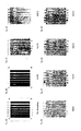
- the above method for forming the electrode in which after the n-electrode and the p-electrode are subjected to the heat treatment, the Au layer is formed again on each electrode and the heat treatment is not performed after that is the most reliable solution, but in this method, the number of steps of forming the electrode is increased, and Au consumption is increased, so that the problem is that the production cost becomes high.
- the present invention was made in view of the above problems, and an object of the present invention is to prevent Au from being alloyed on an n-electrode surface and a p-electrode surface, in a nitride semiconductor element.
- the present invention provides a nitride semiconductor element including a base structure part, an element structure part having at least an n-type AlGaN based semiconductor layer and a p-type AlGaN based semiconductor layer formed on the base structure part, an n-electrode contact part formed on the n-type AlGaN based semiconductor layer, an n-electrode pad part formed on the n-electrode contact part, and a p-electrode formed on the p-type AlGaN based semiconductor layer, in which an AlN mole fraction of the n-type AlGaN based semiconductor layer is 20% or more, the n-electrode contact part includes one or more metal layers, and the p-electrode and the n-electrode pad part have a common laminated structure of two or more layers having an Au layer as an uppermost layer, and an Au diffusion preventing layer composed of conductive metal oxide and formed under the uppermost layer to prevent Au diffusion
- the n-electrode includes the n-electrode contact part and the n-electrode pad part
- the p-electrode has the laminated structure common to the n-electrode pad part, so that the n-electrode and p-electrode can be formed such that after the n-electrode contact part is deposited and patterned on the n-type AlGaN based semiconductor layer, and then annealed, the p-electrode and the n-electrode pad part are deposited and patterned on the p-type AlGaN based semiconductor layer and the n-electrode contact part, respectively at the same time, and then annealed.
- the nitride semiconductor element is the ultraviolet light emitting element, and also it is the rear-face output type light emitting element using flip-chip bonding, the light reflected by the rear-face toward the inside of the element can be reflected again by the n-electrode toward the rear-face side, so that external quantum efficiency of the light emitting element is improved.
- the Au diffusion preventing layer is an ITO layer, in the nitride semiconductor element having the above characteristics.
- the n-electrode contact part does not contain Au, in the nitride semiconductor element having the above characteristics.
- Au consumption required for forming the n-electrode can be reduced.
- a conductive bonding layer is provided between the Au layer as the uppermost layer and the Au diffusion preventing layer in the common laminated structure to bond the Au layer and the Au diffusion preventing layer, and a film thickness of the conductive bonding layer is equal to or less than a half of a film thickness of the Au layer, in the nitride semiconductor element having the above characteristics.
- the Au layer can be prevented from being peeled.
- the film thickness of the conductive bonding layer is equal to or less than a half of the film thickness of the Au layer, so that even when the Au layer is alloyed with the conductive bonding layer to some extent, the Au is prevented from being diffused toward the lower layer of the Au diffusion preventing layer. Consequently, Au erosion does not proceed, and the Au layer on the electrode surface can be kept in the bonding-capable state.
- the present invention provides a method for producing the nitride semiconductor element having the above characteristics, and the method includes a step of forming the base structure part, a step of forming the light emitting element structure part, a step of forming the n-electrode contact part on the n-type AlGaN based semiconductor layer by depositing and patterning a metal layer of the n-electrode contact part, and then performing a first annealing process, and a step of forming the n-electrode pad part on the n-electrode contact part, and the p-electrode on the p-type AlGaN based semiconductor layer at the same time by depositing and patterning a multilayer film of the common laminated structure, and then performing a second annealing process.
- the common laminated structure of the p-electrode and the n-electrode pad part has the Au diffusion preventing layer to prevent the Au diffusion, so that Au can be prevented from being diffused and alloyed at the time of the second annealing process performed when the p-electrode and the n-electrode pad part are formed. That is, compared with the conventional method in which the p-electrode and the n-electrode are separately deposited, patterned, and annealed to be formed, the Au can be prevented from being alloyed without increasing the number of the producing steps.
- the p-electrode can be formed at the same time as the n-electrode pad part in the process for forming the n-electrode, so that compared with the conventional case where the p-electrode and the n-electrode are separately formed, Au can be prevented from being alloyed without increasing the number of the producing steps.
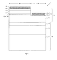
- a light emitting element 1 has a laminated structure in which a substrate is used as a template 5 provided such that an AlN layer 3 and an AlGaN layer 4 are grown on a sapphire substrate 2 (corresponding to a base structure part), and on this template 5, an n-type clad layer 6 composed of n-type AlGaN, an active layer 7, an electron block layer 8 composed of p-type AlGaN having a Al mole fraction higher than the active layer 7, a p-type clad layer 9 composed of p-type AlGaN, and a p-type contact layer 10 composed of p-type GaN are sequentially laminated.
- a p-electrode 12 is formed on a surface of the p-type contact layer 10
- an n-electrode 13 is formed on a part of a surface of a second region R2 other than the first region R1 in the n-type clad layer 6.
- AlN mole fractions of the n-type AlGaN layer and the active layer that is, those of the AlGaN layer 4, the n-type clad layer 6, and the electron block layer 8 are 20% or more and 100% or less, and the AlN mole fraction of the active layer 7 is 0% or more and 80% or less.
- a peak emission wavelength of the light emitting element 1 is 223 nm or more and 365 nm or less.
- the light emitting element is a rear-face output type light emitting element in which light emitted from the well layer 7b is outputted from the sapphire substrate 2, so that the AlN mole fraction of the AlGaN layer 4 needs to be set higher than that of the well layer 7b, and the AlN mole fraction of the AlGaN layer 4 is set to be equal to that of the n-type clad layer 6, as one example.
- the AlN mole fraction of the AlGaN layer 4 may be higher than that of the n-type clad layer 6.
- the n-type clad layer 6 is 2000 nm
- the electron block layer 8 is 2 nm
- the p-type clad layer 9 is 540 nm
- the p-type contact layer 10 is 200 nm in thickness, for example.
- a film thickness of the AlN layer 3 is set to 2200 nm or more and 6600 nm or less, and more preferably 3000 nm or more and 6000 nm or less
- a film thickness of the AlGaN layer 4 is set to 200 nm or more and 300 nm or less.
- the conductivity type of the AlGaN layer 4 may be an n-type layer instead of the undoped layer, so that the AlGaN layer 4 may be integrated with the n-type clad layer 6, and the template 5 may only include the AlN layer 3.
- the n-electrode contact part 13a includes one or more metal layers, and each of the n-electrode pad part 13b and the p-electrode 12 has a bonding Au layer 14 as an uppermost layer, and an Au diffusion preventing layer 15 composed of conductive metal oxide to prevent diffusing of Au, on a lower layer side of the Au layer 14, which is a second characteristic.
- one preferable example of the n-electrode contact part 13a has a three-layer structure in which Ti/Al/Ti having film thicknesses of 10 nm/100 nm/50 nm, respectively are laminated from a lower layer side.
- one preferable example of the n-electrode pad part 13b and the p-electrode 12 has a four-layer structure (common laminated structure) in which Ni/ITO/Ni/Au having film thicknesses of 60 nm/100 nm/10 nm/200 nm, respectively are laminated from a lower layer side.
- ITO indium tin oxide
- the Au diffusion preventing layer 15 may be composed of another conductive metal oxide such as ZnO or NiO instead of ITO.
- a Ni layer 17 formed on the ITO layer 15 functions as a bonding layer to ensure bonding properties between the Au layer 14 and the ITO layer 15, so that several nm is enough for its film thickness, and 10 nm is set in this embodiment.
- the Ni layer 17 as the bonding layer is increased, the Ni layer 17 is alloyed with the Au layer 14, so that the thickness is preferably to be equal to or less than half of a film thickness of the Au layer 14 at most.
- the Ni layer 17 as the bonding layer may be omitted.
- the layers in the template 5 and the light emitting element structure part 11 in the light emitting element 1 are formed by the well-known growing method as described above (steps #1 and #2).
- a first photoresist serving as a reverse pattern of the n-electrode 13 is formed (step #3A), and a Ti/Al/Ti multilayer film serving as the n-electrode contact part 13a is deposited on a whole surface by electron beam evaporation method or the like (step #3B).
- a second photoresist serving as a reverse pattern of the p-electrode 12 and the n-electrode 13 is formed (step #4A), and a Ni/ITO/Ni/Au multilayer film serving as the p-electrode 12 and the n-electrode pad part 13b is deposited on the whole surface by electron beam evaporation or the like (step #4B).
- the electrode surface is subjected to dry cleaning by an ashing process (step #5), and a mounting process such as bonding is performed (step #6).
- the electrode structures of the n-electrode and the p-electrode of the working example 1 used in this experiment is the same as the structures shown in Figs. 6A and 6B , and is formed through the processes shown in Fig. 8 .
- processing temperature is 950°C
- a processing time is 60 seconds
- an atmospheric gas is nitrogen.
- a processing temperature is 450°C
- a processing time is 120 seconds
- an atmospheric gas is air.
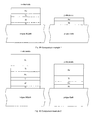
- Fig. 9A shows electrode structures of an n-electrode and a p-electrode in the comparison example 1 used in this experiment
- Fig. 9B shows electrode structures of an n-electrode and a p-electrode in the comparison example 2 used in this experiment.
- the electrode structures are provided such that the n-electrode having a four-layer structure of Ti/Al/Ti/Au and the p-electrode having a two-layer structure of Ni/Au are formed and subjected to the annealing process separately.
- Film thicknesses of the layers of the n-electrode in the comparison example 1 are 10 nm/100 nm/50 nm/100 nm from a lower layer side, and a processing temperature, a processing time, and an atmospheric gas in the annealing process of the n-electrode are the same as those of the first annealing process in the working example 1.
- Film thicknesses of the layers of the p-electrode in the comparison example 1 are 60 nm/50 nm from a lower surface side, and a processing temperature, a processing time, and an atmospheric gas in an annealing process of the p-electrode are the same as those of the second annealing process in the working example 1.
- each of the p-electrode 12 and the n-electrode 13 is not limited to the specific example of the above embodiment, so that the patterning for each of the n-electrode contact part 13a, the p-electrode 12, and the n-electrode pad part 13b is not limited to the liftoff method, and an etching method may be used.
- the etching method the deposition of each multilayer film, the formation of the photoresist, and the etching order are to be conformed to the well-known etching method, and the pattern of the n-electrode contact part 13a may be formed to be larger than the n-electrode 13.
- the nitride semiconductor element according to the present invention is the ultraviolet light emitting element, and furthermore the light emitting diode, but the electrode structure and the method for producing the same described in the above embodiment can be applied to a laser diode, and furthermore can be applied to an ultraviolet light receiving element.
- the nitride semiconductor element according to the present invention can be applied to a light emitting diode or the like in which an AlN mole fraction of an n-type clad layer is 20% or more, and is useful in improving surface texture of each of a p-electrode and an n-electrode.
Landscapes
- Led Devices (AREA)
- Electrodes Of Semiconductors (AREA)
Applications Claiming Priority (1)
| Application Number | Priority Date | Filing Date | Title |
|---|---|---|---|
| PCT/JP2011/072524 WO2013046419A1 (fr) | 2011-09-30 | 2011-09-30 | Élément semi-conducteur nitrure et son procédé de production |
Publications (3)
| Publication Number | Publication Date |
|---|---|
| EP2763192A1 true EP2763192A1 (fr) | 2014-08-06 |
| EP2763192A4 EP2763192A4 (fr) | 2015-06-24 |
| EP2763192B1 EP2763192B1 (fr) | 2019-12-25 |
Family
ID=47994526
Family Applications (1)
| Application Number | Title | Priority Date | Filing Date |
|---|---|---|---|
| EP11873108.2A Active EP2763192B1 (fr) | 2011-09-30 | 2011-09-30 | Élément semi-conducteur nitrure et son procédé de production |
Country Status (7)
| Country | Link |
|---|---|
| US (1) | US9281439B2 (fr) |
| EP (1) | EP2763192B1 (fr) |
| JP (1) | JP5732140B2 (fr) |
| KR (1) | KR101568624B1 (fr) |
| RU (1) | RU2566383C1 (fr) |
| TW (1) | TWI501425B (fr) |
| WO (1) | WO2013046419A1 (fr) |
Families Citing this family (35)
| Publication number | Priority date | Publication date | Assignee | Title |
|---|---|---|---|---|
| US9412911B2 (en) | 2013-07-09 | 2016-08-09 | The Silanna Group Pty Ltd | Optical tuning of light emitting semiconductor junctions |
| EP2881982B1 (fr) * | 2013-12-05 | 2019-09-04 | IMEC vzw | Procédé de fabrication de couches de contact compatibles CMOS dans des dispositifs à semi-conducteurs |
| JP6206159B2 (ja) * | 2013-12-17 | 2017-10-04 | 三菱電機株式会社 | 半導体装置の製造方法 |
| JP6817072B2 (ja) | 2014-05-27 | 2021-01-20 | シランナ・ユー・ブイ・テクノロジーズ・プライベート・リミテッドSilanna Uv Technologies Pte Ltd | 光電子デバイス |
| US11322643B2 (en) | 2014-05-27 | 2022-05-03 | Silanna UV Technologies Pte Ltd | Optoelectronic device |
| KR102318317B1 (ko) | 2014-05-27 | 2021-10-28 | 실라나 유브이 테크놀로지스 피티이 리미티드 | 반도체 구조물과 초격자를 사용하는 진보된 전자 디바이스 구조 |
| KR102427203B1 (ko) | 2014-05-27 | 2022-07-29 | 실라나 유브이 테크놀로지스 피티이 리미티드 | n-형 및 p-형 초격자를 포함하는 전자 디바이스 |
| KR20160025455A (ko) | 2014-08-27 | 2016-03-08 | 서울바이오시스 주식회사 | 발광 소자 및 이의 제조 방법 |
| WO2016032193A1 (fr) * | 2014-08-27 | 2016-03-03 | 서울바이오시스 주식회사 | Diode électroluminescente et son procédé de fabrication |
| JP6330604B2 (ja) * | 2014-09-24 | 2018-05-30 | 日亜化学工業株式会社 | 半導体発光素子 |
| JP5953447B1 (ja) * | 2015-02-05 | 2016-07-20 | Dowaエレクトロニクス株式会社 | Iii族窒化物半導体発光素子およびその製造方法 |
| JP6832620B2 (ja) * | 2015-07-17 | 2021-02-24 | スタンレー電気株式会社 | 窒化物半導体発光素子 |
| US10418517B2 (en) | 2016-02-23 | 2019-09-17 | Silanna UV Technologies Pte Ltd | Resonant optical cavity light emitting device |
| WO2017145026A1 (fr) | 2016-02-23 | 2017-08-31 | Silanna UV Technologies Pte Ltd | Dispositif électroluminescent à cavité optique résonante |
| TWI746596B (zh) * | 2016-08-25 | 2021-11-21 | 晶元光電股份有限公司 | 發光元件 |
| US10804435B2 (en) * | 2016-08-25 | 2020-10-13 | Epistar Corporation | Light-emitting device |
| JP7060508B2 (ja) * | 2016-08-26 | 2022-04-26 | スタンレー電気株式会社 | Iii族窒化物半導体発光素子および該素子構成を含むウエハ |
| JP2018085456A (ja) | 2016-11-24 | 2018-05-31 | 日機装株式会社 | 半導体発光素子の製造方法 |
| JP6404890B2 (ja) * | 2016-11-24 | 2018-10-17 | 日機装株式会社 | 半導体発光素子の製造方法 |
| US10121932B1 (en) * | 2016-11-30 | 2018-11-06 | The United States Of America As Represented By The Secretary Of The Navy | Tunable graphene light-emitting device |
| KR102849643B1 (ko) | 2016-12-23 | 2025-08-25 | 서울바이오시스 주식회사 | 반도체 발광 소자 |
| JP6674394B2 (ja) * | 2017-02-01 | 2020-04-01 | 日機装株式会社 | 半導体発光素子および半導体発光素子の製造方法 |
| RU2719339C1 (ru) * | 2017-02-15 | 2020-04-17 | Соко Кагаку Ко., Лтд. | Способ изготовления нитридного полупроводникового излучающего ультрафиолетовое излучение элемента и нитридный полупроводниковый излучающий ультрафиолетовое излучение элемент |
| JP2018206817A (ja) * | 2017-05-30 | 2018-12-27 | 豊田合成株式会社 | 発光素子 |
| JP2018206818A (ja) * | 2017-05-30 | 2018-12-27 | 豊田合成株式会社 | 発光素子及びその製造方法 |
| JP7000062B2 (ja) * | 2017-07-31 | 2022-01-19 | Dowaホールディングス株式会社 | Iii族窒化物エピタキシャル基板、電子線励起型発光エピタキシャル基板及びそれらの製造方法、並びに電子線励起型発光装置 |
| JP6640815B2 (ja) * | 2017-10-26 | 2020-02-05 | 日機装株式会社 | 半導体発光素子の製造方法 |
| JP6689244B2 (ja) * | 2017-11-10 | 2020-04-28 | 日機装株式会社 | 半導体発光素子の製造方法 |
| JP7049186B2 (ja) * | 2018-05-29 | 2022-04-06 | 日機装株式会社 | 半導体発光素子および半導体発光素子の製造方法 |
| JP2020021798A (ja) * | 2018-07-31 | 2020-02-06 | 日機装株式会社 | 窒化物半導体発光素子及びその製造方法 |
| US10622514B1 (en) | 2018-10-15 | 2020-04-14 | Silanna UV Technologies Pte Ltd | Resonant optical cavity light emitting device |
| US11227978B2 (en) * | 2018-11-12 | 2022-01-18 | Epistar Corporation | Semiconductor device and package structure |
| TWI821302B (zh) * | 2018-11-12 | 2023-11-11 | 晶元光電股份有限公司 | 半導體元件及其封裝結構 |
| CN112599412A (zh) * | 2020-11-24 | 2021-04-02 | 上海工程技术大学 | 一种防击穿的氮化镓基功率器件制备方法 |
| US12439664B2 (en) * | 2022-06-24 | 2025-10-07 | Wolfspeed, Inc. | Methods of forming ohmic contacts on semiconductor devices with trench/mesa structures |
Family Cites Families (15)
| Publication number | Priority date | Publication date | Assignee | Title |
|---|---|---|---|---|
| JPH118410A (ja) * | 1997-06-18 | 1999-01-12 | Nichia Chem Ind Ltd | n型窒化物半導体の電極 |
| JPH1121804A (ja) * | 1997-07-04 | 1999-01-26 | Fujimura Fume Kan Kk | 歩道版及び該歩道版を使用した歩道施工方法並びに遊歩道の施工方法、階段ブロック及び該階段ブロックを使用した階段施工方法 |
| JP3462720B2 (ja) * | 1997-07-16 | 2003-11-05 | 三洋電機株式会社 | n型窒化物半導体の電極及び前記電極を有する半導体素子並びにその製造方法 |
| JPH11307811A (ja) | 1998-04-16 | 1999-11-05 | Furukawa Electric Co Ltd:The | 紫外光発光素子 |
| CN100421266C (zh) * | 2002-08-29 | 2008-09-24 | 首尔半导体股份有限公司 | 具有多个发光元件的发光装置 |
| JP3950801B2 (ja) | 2003-01-31 | 2007-08-01 | 信越半導体株式会社 | 発光素子及び発光素子の製造方法 |
| US20050218414A1 (en) * | 2004-03-30 | 2005-10-06 | Tetsuzo Ueda | 4H-polytype gallium nitride-based semiconductor device on a 4H-polytype substrate |
| JP2005354040A (ja) | 2004-05-11 | 2005-12-22 | Rohm Co Ltd | 半導体発光素子およびその製法 |
| JP2006128527A (ja) * | 2004-11-01 | 2006-05-18 | Osaka Gas Co Ltd | GaN系化合物半導体の製造方法 |
| JPWO2006104063A1 (ja) | 2005-03-28 | 2008-09-04 | 国立大学法人東京工業大学 | 窒化物系深紫外発光素子およびその製造方法 |
| JP2005340860A (ja) * | 2005-08-12 | 2005-12-08 | Toshiba Electronic Engineering Corp | 半導体発光素子 |
| JP4868821B2 (ja) | 2005-10-21 | 2012-02-01 | 京セラ株式会社 | 窒化ガリウム系化合物半導体及び発光素子 |
| JP2007158262A (ja) | 2005-12-08 | 2007-06-21 | Rohm Co Ltd | 半導体発光素子の製造方法 |
| JP5162909B2 (ja) * | 2006-04-03 | 2013-03-13 | 豊田合成株式会社 | 半導体発光素子 |
| CN102484185B (zh) | 2009-09-07 | 2015-01-21 | 首尔伟傲世有限公司 | 半导体发光二极管及其制造方法 |
-
2011
- 2011-09-30 WO PCT/JP2011/072524 patent/WO2013046419A1/fr not_active Ceased
- 2011-09-30 KR KR1020147005511A patent/KR101568624B1/ko active Active
- 2011-09-30 US US14/344,602 patent/US9281439B2/en active Active
- 2011-09-30 RU RU2014116553/28A patent/RU2566383C1/ru active
- 2011-09-30 EP EP11873108.2A patent/EP2763192B1/fr active Active
- 2011-09-30 JP JP2013535762A patent/JP5732140B2/ja active Active
-
2012
- 2012-08-24 TW TW101130845A patent/TWI501425B/zh active
Also Published As
| Publication number | Publication date |
|---|---|
| US9281439B2 (en) | 2016-03-08 |
| KR101568624B1 (ko) | 2015-11-11 |
| TW201314960A (zh) | 2013-04-01 |
| TWI501425B (zh) | 2015-09-21 |
| EP2763192A4 (fr) | 2015-06-24 |
| US20150048304A1 (en) | 2015-02-19 |
| RU2566383C1 (ru) | 2015-10-27 |
| KR20140043163A (ko) | 2014-04-08 |
| WO2013046419A1 (fr) | 2013-04-04 |
| JPWO2013046419A1 (ja) | 2015-03-26 |
| JP5732140B2 (ja) | 2015-06-10 |
| EP2763192B1 (fr) | 2019-12-25 |
Similar Documents
| Publication | Publication Date | Title |
|---|---|---|
| US9281439B2 (en) | Nitride semiconductor element and method for producing same | |
| JP5251121B2 (ja) | 窒化ガリウム系半導体発光素子及びその製造方法 | |
| CN101165928B (zh) | 多重反射层电极以及含有该电极的化合物半导体发光器件 | |
| EP1540744B1 (fr) | Diode electroluminescente a substrat en carbure de silicium | |
| US8884329B2 (en) | Semiconductor light-emitting element, electrode structure and light-emitting device | |
| KR101041843B1 (ko) | 질화물계 화합물 반도체 발광소자 및 그 제조방법 | |
| US20050035354A1 (en) | Light emiting diodes with current spreading layer | |
| US20060138449A1 (en) | Gallium nitride based light-emitting device | |
| WO2005050748A1 (fr) | Dispositif a semi-conducteur et son procede de fabrication | |
| TW200924239A (en) | Light emitting diodes with a p-type surface bonded to a transparent submount to increase light extraction efficiency | |
| KR101161897B1 (ko) | 질화물 반도체 소자 | |
| JP5608589B2 (ja) | 半導体発光素子および半導体発光素子の製造方法 | |
| US7022550B2 (en) | Methods for forming aluminum-containing p-contacts for group III-nitride light emitting diodes | |
| KR20230015861A (ko) | 반도체 소자 | |
| JP2021097148A (ja) | 半導体発光素子 | |
| JP5471485B2 (ja) | 窒化物半導体素子および窒化物半導体素子のパッド電極の製造方法 | |
| JP5130436B2 (ja) | GaN系半導体発光素子及びその製造方法 | |
| JP2007281037A (ja) | 半導体発光素子及びその製造方法 | |
| TWI260099B (en) | Positive electrode structure and gallium nitride-based compound semiconductor light-emitting device | |
| US7700959B2 (en) | Semiconductor light-emitting device, semiconductor light-emitting apparatus, and method of manufacturing semiconductor light-emitting device | |
| JP4980041B2 (ja) | 半導体発光素子 | |
| KR100635159B1 (ko) | 질화물계 반도체 발광소자 및 그 제조방법 | |
| JP2006013475A (ja) | 正極構造及び窒化ガリウム系化合物半導体発光素子 | |
| JP2005150646A (ja) | 発光素子及びその製造方法 | |
| HK1082594B (en) | Light emitting diode with silicon carbide substrate |
Legal Events
| Date | Code | Title | Description |
|---|---|---|---|
| PUAI | Public reference made under article 153(3) epc to a published international application that has entered the european phase |
Free format text: ORIGINAL CODE: 0009012 |
|
| 17P | Request for examination filed |
Effective date: 20140310 |
|
| AK | Designated contracting states |
Kind code of ref document: A1 Designated state(s): AL AT BE BG CH CY CZ DE DK EE ES FI FR GB GR HR HU IE IS IT LI LT LU LV MC MK MT NL NO PL PT RO RS SE SI SK SM TR |
|
| DAX | Request for extension of the european patent (deleted) | ||
| RA4 | Supplementary search report drawn up and despatched (corrected) |
Effective date: 20150528 |
|
| RIC1 | Information provided on ipc code assigned before grant |
Ipc: H01L 33/00 20100101ALI20150521BHEP Ipc: H01L 33/32 20100101ALI20150521BHEP Ipc: H01L 33/38 20100101ALN20150521BHEP Ipc: H01L 29/20 20060101ALN20150521BHEP Ipc: H01L 33/40 20100101AFI20150521BHEP Ipc: H01L 29/45 20060101ALI20150521BHEP |
|
| RIC1 | Information provided on ipc code assigned before grant |
Ipc: H01L 33/40 20100101AFI20150710BHEP Ipc: H01L 33/38 20100101ALN20150710BHEP Ipc: H01L 33/32 20100101ALI20150710BHEP Ipc: H01L 33/00 20100101ALI20150710BHEP Ipc: H01L 29/20 20060101ALN20150710BHEP Ipc: H01L 29/45 20060101ALI20150710BHEP |
|
| RAP1 | Party data changed (applicant data changed or rights of an application transferred) |
Owner name: SOKO KAGAKU CO., LTD. |
|
| RIN1 | Information on inventor provided before grant (corrected) |
Inventor name: INAZU, TETSUHIKO Inventor name: NIWA, NORITAKA |
|
| RIN1 | Information on inventor provided before grant (corrected) |
Inventor name: NIWA, NORITAKA Inventor name: INAZU, TETSUHIKO |
|
| RAP1 | Party data changed (applicant data changed or rights of an application transferred) |
Owner name: SOKO KAGAKU CO., LTD. |
|
| GRAP | Despatch of communication of intention to grant a patent |
Free format text: ORIGINAL CODE: EPIDOSNIGR1 |
|
| STAA | Information on the status of an ep patent application or granted ep patent |
Free format text: STATUS: GRANT OF PATENT IS INTENDED |
|
| INTG | Intention to grant announced |
Effective date: 20190710 |
|
| GRAS | Grant fee paid |
Free format text: ORIGINAL CODE: EPIDOSNIGR3 |
|
| GRAA | (expected) grant |
Free format text: ORIGINAL CODE: 0009210 |
|
| STAA | Information on the status of an ep patent application or granted ep patent |
Free format text: STATUS: THE PATENT HAS BEEN GRANTED |
|
| AK | Designated contracting states |
Kind code of ref document: B1 Designated state(s): AL AT BE BG CH CY CZ DE DK EE ES FI FR GB GR HR HU IE IS IT LI LT LU LV MC MK MT NL NO PL PT RO RS SE SI SK SM TR |
|
| REG | Reference to a national code |
Ref country code: GB Ref legal event code: FG4D |
|
| REG | Reference to a national code |
Ref country code: CH Ref legal event code: EP |
|
| REG | Reference to a national code |
Ref country code: AT Ref legal event code: REF Ref document number: 1218085 Country of ref document: AT Kind code of ref document: T Effective date: 20200115 |
|
| REG | Reference to a national code |
Ref country code: DE Ref legal event code: R096 Ref document number: 602011064298 Country of ref document: DE |
|
| REG | Reference to a national code |
Ref country code: IE Ref legal event code: FG4D |
|
| PG25 | Lapsed in a contracting state [announced via postgrant information from national office to epo] |
Ref country code: FI Free format text: LAPSE BECAUSE OF FAILURE TO SUBMIT A TRANSLATION OF THE DESCRIPTION OR TO PAY THE FEE WITHIN THE PRESCRIBED TIME-LIMIT Effective date: 20191225 Ref country code: LT Free format text: LAPSE BECAUSE OF FAILURE TO SUBMIT A TRANSLATION OF THE DESCRIPTION OR TO PAY THE FEE WITHIN THE PRESCRIBED TIME-LIMIT Effective date: 20191225 Ref country code: GR Free format text: LAPSE BECAUSE OF FAILURE TO SUBMIT A TRANSLATION OF THE DESCRIPTION OR TO PAY THE FEE WITHIN THE PRESCRIBED TIME-LIMIT Effective date: 20200326 Ref country code: NO Free format text: LAPSE BECAUSE OF FAILURE TO SUBMIT A TRANSLATION OF THE DESCRIPTION OR TO PAY THE FEE WITHIN THE PRESCRIBED TIME-LIMIT Effective date: 20200325 Ref country code: SE Free format text: LAPSE BECAUSE OF FAILURE TO SUBMIT A TRANSLATION OF THE DESCRIPTION OR TO PAY THE FEE WITHIN THE PRESCRIBED TIME-LIMIT Effective date: 20191225 Ref country code: LV Free format text: LAPSE BECAUSE OF FAILURE TO SUBMIT A TRANSLATION OF THE DESCRIPTION OR TO PAY THE FEE WITHIN THE PRESCRIBED TIME-LIMIT Effective date: 20191225 Ref country code: BG Free format text: LAPSE BECAUSE OF FAILURE TO SUBMIT A TRANSLATION OF THE DESCRIPTION OR TO PAY THE FEE WITHIN THE PRESCRIBED TIME-LIMIT Effective date: 20200325 |
|
| REG | Reference to a national code |
Ref country code: NL Ref legal event code: FP |
|
| REG | Reference to a national code |
Ref country code: LT Ref legal event code: MG4D |
|
| PG25 | Lapsed in a contracting state [announced via postgrant information from national office to epo] |
Ref country code: RS Free format text: LAPSE BECAUSE OF FAILURE TO SUBMIT A TRANSLATION OF THE DESCRIPTION OR TO PAY THE FEE WITHIN THE PRESCRIBED TIME-LIMIT Effective date: 20191225 Ref country code: HR Free format text: LAPSE BECAUSE OF FAILURE TO SUBMIT A TRANSLATION OF THE DESCRIPTION OR TO PAY THE FEE WITHIN THE PRESCRIBED TIME-LIMIT Effective date: 20191225 |
|
| PG25 | Lapsed in a contracting state [announced via postgrant information from national office to epo] |
Ref country code: AL Free format text: LAPSE BECAUSE OF FAILURE TO SUBMIT A TRANSLATION OF THE DESCRIPTION OR TO PAY THE FEE WITHIN THE PRESCRIBED TIME-LIMIT Effective date: 20191225 |
|
| PG25 | Lapsed in a contracting state [announced via postgrant information from national office to epo] |
Ref country code: EE Free format text: LAPSE BECAUSE OF FAILURE TO SUBMIT A TRANSLATION OF THE DESCRIPTION OR TO PAY THE FEE WITHIN THE PRESCRIBED TIME-LIMIT Effective date: 20191225 Ref country code: RO Free format text: LAPSE BECAUSE OF FAILURE TO SUBMIT A TRANSLATION OF THE DESCRIPTION OR TO PAY THE FEE WITHIN THE PRESCRIBED TIME-LIMIT Effective date: 20191225 Ref country code: CZ Free format text: LAPSE BECAUSE OF FAILURE TO SUBMIT A TRANSLATION OF THE DESCRIPTION OR TO PAY THE FEE WITHIN THE PRESCRIBED TIME-LIMIT Effective date: 20191225 Ref country code: PT Free format text: LAPSE BECAUSE OF FAILURE TO SUBMIT A TRANSLATION OF THE DESCRIPTION OR TO PAY THE FEE WITHIN THE PRESCRIBED TIME-LIMIT Effective date: 20200520 |
|
| PG25 | Lapsed in a contracting state [announced via postgrant information from national office to epo] |
Ref country code: IS Free format text: LAPSE BECAUSE OF FAILURE TO SUBMIT A TRANSLATION OF THE DESCRIPTION OR TO PAY THE FEE WITHIN THE PRESCRIBED TIME-LIMIT Effective date: 20200425 Ref country code: SK Free format text: LAPSE BECAUSE OF FAILURE TO SUBMIT A TRANSLATION OF THE DESCRIPTION OR TO PAY THE FEE WITHIN THE PRESCRIBED TIME-LIMIT Effective date: 20191225 Ref country code: SM Free format text: LAPSE BECAUSE OF FAILURE TO SUBMIT A TRANSLATION OF THE DESCRIPTION OR TO PAY THE FEE WITHIN THE PRESCRIBED TIME-LIMIT Effective date: 20191225 |
|
| REG | Reference to a national code |
Ref country code: DE Ref legal event code: R097 Ref document number: 602011064298 Country of ref document: DE |
|
| PG25 | Lapsed in a contracting state [announced via postgrant information from national office to epo] |
Ref country code: ES Free format text: LAPSE BECAUSE OF FAILURE TO SUBMIT A TRANSLATION OF THE DESCRIPTION OR TO PAY THE FEE WITHIN THE PRESCRIBED TIME-LIMIT Effective date: 20191225 Ref country code: DK Free format text: LAPSE BECAUSE OF FAILURE TO SUBMIT A TRANSLATION OF THE DESCRIPTION OR TO PAY THE FEE WITHIN THE PRESCRIBED TIME-LIMIT Effective date: 20191225 |
|
| PLBE | No opposition filed within time limit |
Free format text: ORIGINAL CODE: 0009261 |
|
| STAA | Information on the status of an ep patent application or granted ep patent |
Free format text: STATUS: NO OPPOSITION FILED WITHIN TIME LIMIT |
|
| REG | Reference to a national code |
Ref country code: AT Ref legal event code: MK05 Ref document number: 1218085 Country of ref document: AT Kind code of ref document: T Effective date: 20191225 |
|
| PG25 | Lapsed in a contracting state [announced via postgrant information from national office to epo] |
Ref country code: SI Free format text: LAPSE BECAUSE OF FAILURE TO SUBMIT A TRANSLATION OF THE DESCRIPTION OR TO PAY THE FEE WITHIN THE PRESCRIBED TIME-LIMIT Effective date: 20191225 |
|
| 26N | No opposition filed |
Effective date: 20200928 |
|
| PG25 | Lapsed in a contracting state [announced via postgrant information from national office to epo] |
Ref country code: IT Free format text: LAPSE BECAUSE OF FAILURE TO SUBMIT A TRANSLATION OF THE DESCRIPTION OR TO PAY THE FEE WITHIN THE PRESCRIBED TIME-LIMIT Effective date: 20191225 Ref country code: AT Free format text: LAPSE BECAUSE OF FAILURE TO SUBMIT A TRANSLATION OF THE DESCRIPTION OR TO PAY THE FEE WITHIN THE PRESCRIBED TIME-LIMIT Effective date: 20191225 |
|
| PG25 | Lapsed in a contracting state [announced via postgrant information from national office to epo] |
Ref country code: PL Free format text: LAPSE BECAUSE OF FAILURE TO SUBMIT A TRANSLATION OF THE DESCRIPTION OR TO PAY THE FEE WITHIN THE PRESCRIBED TIME-LIMIT Effective date: 20191225 |
|
| PG25 | Lapsed in a contracting state [announced via postgrant information from national office to epo] |
Ref country code: MC Free format text: LAPSE BECAUSE OF FAILURE TO SUBMIT A TRANSLATION OF THE DESCRIPTION OR TO PAY THE FEE WITHIN THE PRESCRIBED TIME-LIMIT Effective date: 20191225 |
|
| REG | Reference to a national code |
Ref country code: CH Ref legal event code: PL |
|
| GBPC | Gb: european patent ceased through non-payment of renewal fee |
Effective date: 20200930 |
|
| REG | Reference to a national code |
Ref country code: BE Ref legal event code: MM Effective date: 20200930 |
|
| PG25 | Lapsed in a contracting state [announced via postgrant information from national office to epo] |
Ref country code: LU Free format text: LAPSE BECAUSE OF NON-PAYMENT OF DUE FEES Effective date: 20200930 |
|
| PG25 | Lapsed in a contracting state [announced via postgrant information from national office to epo] |
Ref country code: IE Free format text: LAPSE BECAUSE OF NON-PAYMENT OF DUE FEES Effective date: 20200930 Ref country code: LI Free format text: LAPSE BECAUSE OF NON-PAYMENT OF DUE FEES Effective date: 20200930 Ref country code: GB Free format text: LAPSE BECAUSE OF NON-PAYMENT OF DUE FEES Effective date: 20200930 Ref country code: CH Free format text: LAPSE BECAUSE OF NON-PAYMENT OF DUE FEES Effective date: 20200930 Ref country code: BE Free format text: LAPSE BECAUSE OF NON-PAYMENT OF DUE FEES Effective date: 20200930 |
|
| PG25 | Lapsed in a contracting state [announced via postgrant information from national office to epo] |
Ref country code: TR Free format text: LAPSE BECAUSE OF FAILURE TO SUBMIT A TRANSLATION OF THE DESCRIPTION OR TO PAY THE FEE WITHIN THE PRESCRIBED TIME-LIMIT Effective date: 20191225 Ref country code: MT Free format text: LAPSE BECAUSE OF FAILURE TO SUBMIT A TRANSLATION OF THE DESCRIPTION OR TO PAY THE FEE WITHIN THE PRESCRIBED TIME-LIMIT Effective date: 20191225 Ref country code: CY Free format text: LAPSE BECAUSE OF FAILURE TO SUBMIT A TRANSLATION OF THE DESCRIPTION OR TO PAY THE FEE WITHIN THE PRESCRIBED TIME-LIMIT Effective date: 20191225 |
|
| PG25 | Lapsed in a contracting state [announced via postgrant information from national office to epo] |
Ref country code: MK Free format text: LAPSE BECAUSE OF FAILURE TO SUBMIT A TRANSLATION OF THE DESCRIPTION OR TO PAY THE FEE WITHIN THE PRESCRIBED TIME-LIMIT Effective date: 20191225 |
|
| REG | Reference to a national code |
Ref country code: DE Ref legal event code: R081 Ref document number: 602011064298 Country of ref document: DE Owner name: NIKKISO CO., LTD., JP Free format text: FORMER OWNER: SOKO KAGAKU CO., LTD., HAKUSAN-SHI, ISHIKAWA, JP Ref country code: DE Ref legal event code: R081 Ref document number: 602011064298 Country of ref document: DE Owner name: NIKKISO COMPANY LIMITED, JP Free format text: FORMER OWNER: SOKO KAGAKU CO., LTD., HAKUSAN-SHI, ISHIKAWA, JP Ref country code: DE Ref legal event code: R081 Ref document number: 602011064298 Country of ref document: DE Owner name: SOKO KAGAKU CO., LTD., JP Free format text: FORMER OWNER: SOKO KAGAKU CO., LTD., HAKUSAN-SHI, ISHIKAWA, JP |
|
| REG | Reference to a national code |
Ref country code: DE Ref legal event code: R081 Ref document number: 602011064298 Country of ref document: DE Owner name: NIKKISO CO., LTD., JP Free format text: FORMER OWNER: NIKKISO COMPANY LIMITED, TOKYO, JP Ref country code: DE Ref legal event code: R081 Ref document number: 602011064298 Country of ref document: DE Owner name: SOKO KAGAKU CO., LTD., JP Free format text: FORMER OWNER: NIKKISO COMPANY LIMITED, TOKYO, JP |
|
| REG | Reference to a national code |
Ref country code: NL Ref legal event code: PD Owner name: NIKKISO CO., LTD.; JP Free format text: DETAILS ASSIGNMENT: CHANGE OF OWNER(S), ASSIGNMENT; FORMER OWNER NAME: SOKO KAGAKU CO., LTD. Effective date: 20230524 |
|
| REG | Reference to a national code |
Ref country code: DE Ref legal event code: R079 Ref document number: 602011064298 Country of ref document: DE Free format text: PREVIOUS MAIN CLASS: H01L0033400000 Ipc: H10H0020832000 |
|
| PGFP | Annual fee paid to national office [announced via postgrant information from national office to epo] |
Ref country code: DE Payment date: 20250915 Year of fee payment: 15 |
|
| PGFP | Annual fee paid to national office [announced via postgrant information from national office to epo] |
Ref country code: NL Payment date: 20250922 Year of fee payment: 15 |
|
| PGFP | Annual fee paid to national office [announced via postgrant information from national office to epo] |
Ref country code: FR Payment date: 20250925 Year of fee payment: 15 |
|
| REG | Reference to a national code |
Ref country code: DE Ref legal event code: R081 Ref document number: 602011064298 Country of ref document: DE Owner name: SOKO KAGAKU CO., LTD., JP Free format text: FORMER OWNER: NIKKISO CO., LTD., TOKYO, JP |