EP2763518A1 - Corps de montage de substrat à composant intégré, son procédé de fabrication et substrat à composant intégré - Google Patents
Corps de montage de substrat à composant intégré, son procédé de fabrication et substrat à composant intégré Download PDFInfo
- Publication number
- EP2763518A1 EP2763518A1 EP12835560.9A EP12835560A EP2763518A1 EP 2763518 A1 EP2763518 A1 EP 2763518A1 EP 12835560 A EP12835560 A EP 12835560A EP 2763518 A1 EP2763518 A1 EP 2763518A1
- Authority
- EP
- European Patent Office
- Prior art keywords
- board
- thermal
- built
- wiring
- component built
- Prior art date
- Legal status (The legal status is an assumption and is not a legal conclusion. Google has not performed a legal analysis and makes no representation as to the accuracy of the status listed.)
- Withdrawn
Links
Images


Classifications
-
- H—ELECTRICITY
- H05—ELECTRIC TECHNIQUES NOT OTHERWISE PROVIDED FOR
- H05K—PRINTED CIRCUITS; CASINGS OR CONSTRUCTIONAL DETAILS OF ELECTRIC APPARATUS; MANUFACTURE OF ASSEMBLAGES OF ELECTRICAL COMPONENTS
- H05K1/00—Printed circuits
- H05K1/18—Printed circuits structurally associated with non-printed electric components
- H05K1/182—Printed circuits structurally associated with non-printed electric components associated with components mounted in printed circuit boards [PCB], e.g. insert-mounted components [IMC]
- H05K1/185—Printed circuits structurally associated with non-printed electric components associated with components mounted in printed circuit boards [PCB], e.g. insert-mounted components [IMC] associated with components encapsulated in the insulating substrate of the PCBs; associated with components incorporated in internal layers of multilayer circuit boards
-
- H—ELECTRICITY
- H05—ELECTRIC TECHNIQUES NOT OTHERWISE PROVIDED FOR
- H05K—PRINTED CIRCUITS; CASINGS OR CONSTRUCTIONAL DETAILS OF ELECTRIC APPARATUS; MANUFACTURE OF ASSEMBLAGES OF ELECTRICAL COMPONENTS
- H05K1/00—Printed circuits
- H05K1/02—Details
- H05K1/0201—Thermal arrangements, e.g. for cooling, heating or preventing overheating
- H05K1/0203—Cooling of mounted components
- H05K1/0204—Cooling of mounted components using means for thermal conduction connection in the thickness direction of the substrate
- H05K1/0206—Cooling of mounted components using means for thermal conduction connection in the thickness direction of the substrate by printed thermal vias
-
- H—ELECTRICITY
- H05—ELECTRIC TECHNIQUES NOT OTHERWISE PROVIDED FOR
- H05K—PRINTED CIRCUITS; CASINGS OR CONSTRUCTIONAL DETAILS OF ELECTRIC APPARATUS; MANUFACTURE OF ASSEMBLAGES OF ELECTRICAL COMPONENTS
- H05K1/00—Printed circuits
- H05K1/02—Details
- H05K1/0296—Conductive pattern lay-out details not covered by sub groups H05K1/02 - H05K1/0295
- H05K1/0298—Multilayer circuits
-
- H—ELECTRICITY
- H05—ELECTRIC TECHNIQUES NOT OTHERWISE PROVIDED FOR
- H05K—PRINTED CIRCUITS; CASINGS OR CONSTRUCTIONAL DETAILS OF ELECTRIC APPARATUS; MANUFACTURE OF ASSEMBLAGES OF ELECTRICAL COMPONENTS
- H05K1/00—Printed circuits
- H05K1/18—Printed circuits structurally associated with non-printed electric components
- H05K1/182—Printed circuits structurally associated with non-printed electric components associated with components mounted in printed circuit boards [PCB], e.g. insert-mounted components [IMC]
- H05K1/185—Printed circuits structurally associated with non-printed electric components associated with components mounted in printed circuit boards [PCB], e.g. insert-mounted components [IMC] associated with components encapsulated in the insulating substrate of the PCBs; associated with components incorporated in internal layers of multilayer circuit boards
- H05K1/186—Printed circuits structurally associated with non-printed electric components associated with components mounted in printed circuit boards [PCB], e.g. insert-mounted components [IMC] associated with components encapsulated in the insulating substrate of the PCBs; associated with components incorporated in internal layers of multilayer circuit boards manufactured by mounting on or connecting to patterned circuits before or during embedding
-
- H—ELECTRICITY
- H05—ELECTRIC TECHNIQUES NOT OTHERWISE PROVIDED FOR
- H05K—PRINTED CIRCUITS; CASINGS OR CONSTRUCTIONAL DETAILS OF ELECTRIC APPARATUS; MANUFACTURE OF ASSEMBLAGES OF ELECTRICAL COMPONENTS
- H05K3/00—Apparatus or processes for manufacturing printed circuits
- H05K3/30—Assembling printed circuits with electric components, e.g. with resistors
- H05K3/301—Assembling printed circuits with electric components, e.g. with resistors by means of a mounting structure
-
- H—ELECTRICITY
- H10—SEMICONDUCTOR DEVICES; ELECTRIC SOLID-STATE DEVICES NOT OTHERWISE PROVIDED FOR
- H10W—GENERIC PACKAGES, INTERCONNECTIONS, CONNECTORS OR OTHER CONSTRUCTIONAL DETAILS OF DEVICES COVERED BY CLASS H10
- H10W40/00—Arrangements for thermal protection or thermal control
- H10W40/20—Arrangements for cooling
- H10W40/22—Arrangements for cooling characterised by their shape, e.g. having conical or cylindrical projections
- H10W40/226—Arrangements for cooling characterised by their shape, e.g. having conical or cylindrical projections characterised by projecting parts, e.g. fins to increase surface area
- H10W40/228—Arrangements for cooling characterised by their shape, e.g. having conical or cylindrical projections characterised by projecting parts, e.g. fins to increase surface area the projecting parts being wire-shaped or pin-shaped
-
- H—ELECTRICITY
- H10—SEMICONDUCTOR DEVICES; ELECTRIC SOLID-STATE DEVICES NOT OTHERWISE PROVIDED FOR
- H10W—GENERIC PACKAGES, INTERCONNECTIONS, CONNECTORS OR OTHER CONSTRUCTIONAL DETAILS OF DEVICES COVERED BY CLASS H10
- H10W70/00—Package substrates; Interposers; Redistribution layers [RDL]
- H10W70/60—Insulating or insulated package substrates; Interposers; Redistribution layers
- H10W70/611—Insulating or insulated package substrates; Interposers; Redistribution layers for connecting multiple chips together
- H10W70/614—Insulating or insulated package substrates; Interposers; Redistribution layers for connecting multiple chips together the multiple chips being integrally enclosed
-
- H—ELECTRICITY
- H10—SEMICONDUCTOR DEVICES; ELECTRIC SOLID-STATE DEVICES NOT OTHERWISE PROVIDED FOR
- H10W—GENERIC PACKAGES, INTERCONNECTIONS, CONNECTORS OR OTHER CONSTRUCTIONAL DETAILS OF DEVICES COVERED BY CLASS H10
- H10W74/00—Encapsulations, e.g. protective coatings
- H10W74/10—Encapsulations, e.g. protective coatings characterised by their shape or disposition
- H10W74/111—Encapsulations, e.g. protective coatings characterised by their shape or disposition the semiconductor body being completely enclosed
- H10W74/114—Encapsulations, e.g. protective coatings characterised by their shape or disposition the semiconductor body being completely enclosed by a substrate and the encapsulations
-
- H—ELECTRICITY
- H10—SEMICONDUCTOR DEVICES; ELECTRIC SOLID-STATE DEVICES NOT OTHERWISE PROVIDED FOR
- H10W—GENERIC PACKAGES, INTERCONNECTIONS, CONNECTORS OR OTHER CONSTRUCTIONAL DETAILS OF DEVICES COVERED BY CLASS H10
- H10W90/00—Package configurations
- H10W90/401—Package configurations characterised by multiple insulating or insulated package substrates, interposers or RDLs
-
- H—ELECTRICITY
- H05—ELECTRIC TECHNIQUES NOT OTHERWISE PROVIDED FOR
- H05K—PRINTED CIRCUITS; CASINGS OR CONSTRUCTIONAL DETAILS OF ELECTRIC APPARATUS; MANUFACTURE OF ASSEMBLAGES OF ELECTRICAL COMPONENTS
- H05K2203/00—Indexing scheme relating to apparatus or processes for manufacturing printed circuits covered by H05K3/00
- H05K2203/14—Related to the order of processing steps
- H05K2203/1453—Applying the circuit pattern before another process, e.g. before filling of vias with conductive paste, before making printed resistors
-
- H—ELECTRICITY
- H05—ELECTRIC TECHNIQUES NOT OTHERWISE PROVIDED FOR
- H05K—PRINTED CIRCUITS; CASINGS OR CONSTRUCTIONAL DETAILS OF ELECTRIC APPARATUS; MANUFACTURE OF ASSEMBLAGES OF ELECTRICAL COMPONENTS
- H05K3/00—Apparatus or processes for manufacturing printed circuits
- H05K3/0011—Working of insulating substrates or insulating layers
- H05K3/0017—Etching of the substrate by chemical or physical means
- H05K3/0026—Etching of the substrate by chemical or physical means by laser ablation
-
- H—ELECTRICITY
- H05—ELECTRIC TECHNIQUES NOT OTHERWISE PROVIDED FOR
- H05K—PRINTED CIRCUITS; CASINGS OR CONSTRUCTIONAL DETAILS OF ELECTRIC APPARATUS; MANUFACTURE OF ASSEMBLAGES OF ELECTRICAL COMPONENTS
- H05K3/00—Apparatus or processes for manufacturing printed circuits
- H05K3/40—Forming printed elements for providing electric connections to or between printed circuits
- H05K3/4038—Through-connections; Vertical interconnect access [VIA] connections
-
- H—ELECTRICITY
- H05—ELECTRIC TECHNIQUES NOT OTHERWISE PROVIDED FOR
- H05K—PRINTED CIRCUITS; CASINGS OR CONSTRUCTIONAL DETAILS OF ELECTRIC APPARATUS; MANUFACTURE OF ASSEMBLAGES OF ELECTRICAL COMPONENTS
- H05K3/00—Apparatus or processes for manufacturing printed circuits
- H05K3/40—Forming printed elements for providing electric connections to or between printed circuits
- H05K3/4038—Through-connections; Vertical interconnect access [VIA] connections
- H05K3/4053—Through-connections; Vertical interconnect access [VIA] connections by thick-film techniques
-
- H—ELECTRICITY
- H05—ELECTRIC TECHNIQUES NOT OTHERWISE PROVIDED FOR
- H05K—PRINTED CIRCUITS; CASINGS OR CONSTRUCTIONAL DETAILS OF ELECTRIC APPARATUS; MANUFACTURE OF ASSEMBLAGES OF ELECTRICAL COMPONENTS
- H05K3/00—Apparatus or processes for manufacturing printed circuits
- H05K3/40—Forming printed elements for providing electric connections to or between printed circuits
- H05K3/42—Plated through-holes or plated via connections
- H05K3/429—Plated through-holes specially for multilayer circuits, e.g. having connections to inner circuit layers
-
- H—ELECTRICITY
- H05—ELECTRIC TECHNIQUES NOT OTHERWISE PROVIDED FOR
- H05K—PRINTED CIRCUITS; CASINGS OR CONSTRUCTIONAL DETAILS OF ELECTRIC APPARATUS; MANUFACTURE OF ASSEMBLAGES OF ELECTRICAL COMPONENTS
- H05K3/00—Apparatus or processes for manufacturing printed circuits
- H05K3/46—Manufacturing multilayer circuits
- H05K3/4611—Manufacturing multilayer circuits by laminating two or more circuit boards
- H05K3/4614—Manufacturing multilayer circuits by laminating two or more circuit boards the electrical connections between the circuit boards being made during lamination
-
- H—ELECTRICITY
- H05—ELECTRIC TECHNIQUES NOT OTHERWISE PROVIDED FOR
- H05K—PRINTED CIRCUITS; CASINGS OR CONSTRUCTIONAL DETAILS OF ELECTRIC APPARATUS; MANUFACTURE OF ASSEMBLAGES OF ELECTRICAL COMPONENTS
- H05K3/00—Apparatus or processes for manufacturing printed circuits
- H05K3/46—Manufacturing multilayer circuits
- H05K3/4611—Manufacturing multilayer circuits by laminating two or more circuit boards
- H05K3/4614—Manufacturing multilayer circuits by laminating two or more circuit boards the electrical connections between the circuit boards being made during lamination
- H05K3/4617—Manufacturing multilayer circuits by laminating two or more circuit boards the electrical connections between the circuit boards being made during lamination characterized by laminating only or mainly similar single-sided circuit boards
-
- H—ELECTRICITY
- H05—ELECTRIC TECHNIQUES NOT OTHERWISE PROVIDED FOR
- H05K—PRINTED CIRCUITS; CASINGS OR CONSTRUCTIONAL DETAILS OF ELECTRIC APPARATUS; MANUFACTURE OF ASSEMBLAGES OF ELECTRICAL COMPONENTS
- H05K3/00—Apparatus or processes for manufacturing printed circuits
- H05K3/46—Manufacturing multilayer circuits
- H05K3/4611—Manufacturing multilayer circuits by laminating two or more circuit boards
- H05K3/4614—Manufacturing multilayer circuits by laminating two or more circuit boards the electrical connections between the circuit boards being made during lamination
- H05K3/462—Manufacturing multilayer circuits by laminating two or more circuit boards the electrical connections between the circuit boards being made during lamination characterized by laminating only or mainly similar double-sided circuit boards
-
- H—ELECTRICITY
- H05—ELECTRIC TECHNIQUES NOT OTHERWISE PROVIDED FOR
- H05K—PRINTED CIRCUITS; CASINGS OR CONSTRUCTIONAL DETAILS OF ELECTRIC APPARATUS; MANUFACTURE OF ASSEMBLAGES OF ELECTRICAL COMPONENTS
- H05K3/00—Apparatus or processes for manufacturing printed circuits
- H05K3/46—Manufacturing multilayer circuits
- H05K3/4611—Manufacturing multilayer circuits by laminating two or more circuit boards
- H05K3/4623—Manufacturing multilayer circuits by laminating two or more circuit boards the circuit boards having internal via connections between two or more circuit layers before lamination, e.g. double-sided circuit boards
-
- H—ELECTRICITY
- H10—SEMICONDUCTOR DEVICES; ELECTRIC SOLID-STATE DEVICES NOT OTHERWISE PROVIDED FOR
- H10W—GENERIC PACKAGES, INTERCONNECTIONS, CONNECTORS OR OTHER CONSTRUCTIONAL DETAILS OF DEVICES COVERED BY CLASS H10
- H10W74/00—Encapsulations, e.g. protective coatings
- H10W74/10—Encapsulations, e.g. protective coatings characterised by their shape or disposition
- H10W74/15—Encapsulations, e.g. protective coatings characterised by their shape or disposition on active surfaces of flip-chip devices, e.g. underfills
-
- H—ELECTRICITY
- H10—SEMICONDUCTOR DEVICES; ELECTRIC SOLID-STATE DEVICES NOT OTHERWISE PROVIDED FOR
- H10W—GENERIC PACKAGES, INTERCONNECTIONS, CONNECTORS OR OTHER CONSTRUCTIONAL DETAILS OF DEVICES COVERED BY CLASS H10
- H10W90/00—Package configurations
- H10W90/701—Package configurations characterised by the relative positions of pads or connectors relative to package parts
-
- H—ELECTRICITY
- H10—SEMICONDUCTOR DEVICES; ELECTRIC SOLID-STATE DEVICES NOT OTHERWISE PROVIDED FOR
- H10W—GENERIC PACKAGES, INTERCONNECTIONS, CONNECTORS OR OTHER CONSTRUCTIONAL DETAILS OF DEVICES COVERED BY CLASS H10
- H10W90/00—Package configurations
- H10W90/701—Package configurations characterised by the relative positions of pads or connectors relative to package parts
- H10W90/721—Package configurations characterised by the relative positions of pads or connectors relative to package parts of bump connectors
- H10W90/724—Package configurations characterised by the relative positions of pads or connectors relative to package parts of bump connectors between a chip and a stacked insulating package substrate, interposer or RDL
-
- H—ELECTRICITY
- H10—SEMICONDUCTOR DEVICES; ELECTRIC SOLID-STATE DEVICES NOT OTHERWISE PROVIDED FOR
- H10W—GENERIC PACKAGES, INTERCONNECTIONS, CONNECTORS OR OTHER CONSTRUCTIONAL DETAILS OF DEVICES COVERED BY CLASS H10
- H10W90/00—Package configurations
- H10W90/701—Package configurations characterised by the relative positions of pads or connectors relative to package parts
- H10W90/731—Package configurations characterised by the relative positions of pads or connectors relative to package parts of die-attach connectors
- H10W90/734—Package configurations characterised by the relative positions of pads or connectors relative to package parts of die-attach connectors between a chip and a stacked insulating package substrate, interposer or RDL
-
- Y—GENERAL TAGGING OF NEW TECHNOLOGICAL DEVELOPMENTS; GENERAL TAGGING OF CROSS-SECTIONAL TECHNOLOGIES SPANNING OVER SEVERAL SECTIONS OF THE IPC; TECHNICAL SUBJECTS COVERED BY FORMER USPC CROSS-REFERENCE ART COLLECTIONS [XRACs] AND DIGESTS
- Y10—TECHNICAL SUBJECTS COVERED BY FORMER USPC
- Y10T—TECHNICAL SUBJECTS COVERED BY FORMER US CLASSIFICATION
- Y10T29/00—Metal working
- Y10T29/49—Method of mechanical manufacture
- Y10T29/49002—Electrical device making
- Y10T29/49117—Conductor or circuit manufacturing
- Y10T29/49124—On flat or curved insulated base, e.g., printed circuit, etc.
- Y10T29/4913—Assembling to base an electrical component, e.g., capacitor, etc.
Definitions
- This invention relates to a component built-in board mounting body in which a component built-in board having an electronic component built in thereto is mounted on a mounting board, and a method of manufacturing the same, and to a component built-in board.
- Tj temperature semiconductor element temperature
- the semiconductor element itself is destroyed, hence thermal design is performed such that Tj temperature is inarangeof 80°C to 100°C.
- structural design taking account of heat radiation characteristics is important since a periphery of the built in electronic component (IC chip or passive component) is covered by an insulating resin material (for example, an epoxy resin or polyimide resin whose heat transmission coefficient is approximately 0.2 W/mk).
- the insulating resin material has a heat transmission coefficient which is about one thousandth (1/1000) compared to that of a wiring metal material (for example, copper whose heat transmission coefficient is approximately 370 W/mk).
- a known electronic component built-in type wiring board that takes account of heat radiation characteristics in this way is the electronic component built-in type wiring board disclosed in Patent Document 1 identified below.
- This electronic component built-in type wiring board has a structure in which by forming a thermal via on a surface on an opposite side to an electrode formation surface of the built in electronic component, heat of the electronic component is radiated from this thermal via to external air via a heat radiation board in a surface layer.
- Patent Document 1 Unexamined Japanese Patent Application Publication No. JP 2008-205124 A
- the electronic component built-in type wiring board disclosed in above-described Patent Document 1 has a structure in which heat is radiated via the thermal via and the heat radiation board only to external air. Hence, it cannot say that heat radiation characteristics of the electronic component have been sufficiently improved, and there is room for further improvement in heat radiation characteristics to be achieved.
- overall thickness of the board ends up increasing by an amount of thickness of the heat radiation board. Hence, for example, when mounted on a mounting board, overall height increases and it cannot say that the structure is sufficiently responding to the requirements of miniaturization, and so on.
- the heat radiation board needs to be disposed in a close vicinity of the electronic component. Hence, there is a problem that flexibility of layout of the electronic component is limited.
- An object of the invention is to overcome the above-mentioned problems due to the conventional technology, to provide a component built-in board mounting body, which is capable of miniaturization, has high flexibility of layout of the built in electronic component, and makes itpossibletoachievean improvement in heat radiation characteristics of the electronic component built in to the component built-in board, a method of manufacturing the component built-in board mounting body and a component built-in board.
- a component built-in board mounting body has a component built-in board mounted on a mounting surface of a mounting board, the component built-in board being configured having stacked therein a plurality of printed wiring bases that each have a wiring pattern and a via formed on/in a resin base thereof, and the component built-in board being configured having an electronic component built in thereto, wherein the component built-in board has at least a portion of the plurality of printed wiring bases including thermal wiring in the wiring pattern and including a thermal via in the via, and the component built-in board is mounted on the mounting board via a bump formed on a surface layer of the component built-in board, and a surface on an opposite side to an electrode formation surface of the built in electronic component is connected to the bump via the thermal via and the thermal wiring, and is thermally connected to the mounting board via the bump.
- the surface on the opposite side to the electrode formation surface of the electronic component built in to the component built-in board is connected to the mounting board via the thermal via, the thermal wiring, and the bump formed on the surface layer of the component built-in board. Therefore, heat of the electronic component is transmitted along the thermal via, the thermal wiring, and the bump that act as a heat radiation path, to be radiated efficiently and reliably to the mounting board.
- the mounting board has a sufficiently large surface area compared to the electronic component or the component built-in board, hence is better than a heat radiation board as a heat radiation medium, and there is no need to provide a conventional kind of heat radiation board. As a result, miniaturization is possible, and it is possible to achieve improvement in heat radiation characteristics of the built in electronic component while increasing flexibility of layout of the electronic component.
- the electronic component is disposed between the thermal wiring and the mounting board in a stacking direction of the printed wiring bases.
- the thermal wiring is disposed between the electronic component and the mounting board in the stacking direction of the printed wiring bases.
- a method of manufacturing a component built-in board mounting body comprises the steps of: forming the wiring pattern including thermal wiring and the via including a thermal via in a plurality of the resin bases, and forming in at least one of the plurality of resin bases an opening where the electronic component is built in, thereby forming the plurality of printed wiring bases; collectively stacking the plurality of printed wiring bases by thermal compression bonding such that a surface on an opposite side to an electrode formation surface of the electronic component is connected to the thermal wiring via the thermal via, thereby forming the component built-in board; forming on a surface layer of the component built-in board a bump connected to the thermal wiring; and mounting
- the surface on the opposite side to the electrode formation surface of the electronic component built in to the component built-in board is connected to the thermal wiring via the thermal via, and the bump connected to the thermal wiring is formed on the surface layer of the component built- in board to perform mounting on the mounting board, hence working effects similar to those described above can be displayed.
- a component built-in board is configured having stacked therein a plurality of printed wiring bases each having a wiring pattern and a via formed on/in a resin base thereof, and is configured having an electronic component built in thereto, wherein at least a portion of the plurality of printed wiring bases include thermal wiring in the wiring pattern and include a thermal via in the via, and the component built-in board is mounted on a mounting board via a bump formed on a surface layer of the component built-in board, and a surface on an opposite side to an electrode formation surface of the built in electronic component is connected to the bump via the thermal via and the thermal wiring.
- the surface on the opposite side to the electrode formation surface of the built in electronic component is connected to the bump of the surface layer via the thermal via and the thermal wiring and is therefore thermally connected to the mounting board via this bump, thereby making it possible to achieve improvement in heat radiation characteristics of the built in electronic component.
- a component built-in board mounting body has a component built-in board mounted on a mounting surface of a mounting board, the component built-in board being configured having stacked therein a plurality of printed wiring bases that each have a wiring pattern and a via formed on/in a resin base thereof, and the component built-in board being configured having a first electronic component built in thereto and a second electronic component surface-mounted thereon, wherein the component built-in board has at least a portion of the plurality of printed wiring bases including thermal wiring in the wiring pattern and including a thermal via in the via, the component built-in board is mounted on the mounting board via a first bump formed on one of surface layers of the component built-in board and has the second electronic component surface-mounted thereon via a second bump formed on the other of the surface layers of the component built-inboard, an electrode of the first electronic component is connected to the second bump via the via and the wiring pattern, and a surface on an opposite side to a formation surface of the electrode is connected to the first bump via
- the surface on the opposite side to the formation surface of the electrode of the first electronic component built in to the component built-in board is connected to the mounting board via the thermal via, the thermal wiring, and the first bump formed on one of the surface layers of the component built-in board, and the electrode of the first electronic component is connected to the surface-mounted second electronic component via the via, the wiring pattern, and the second bump formed on the other of the surface layers of the component built-in board. Therefore, heat of the built in first electronic component is transmitted along the thermal via, the thermal wiring, and the first bump that act as a heat radiation path, to be radiated efficiently and reliably to the mounting board.
- heat of the surface-mounted second electronic component is transmitted mainly along the second bump, the wiring pattern, the via, the first electronic component, the thermal via, the thermal wiring, and the first bump that act as a heat radiation path, to be similarly radiated efficiently and reliably to the mounting board.
- the mounting board has a sufficiently large surface area compared to each of the electronic components or the component built-in board, hence is better than a heat radiation board as a heat radiation medium, and there is no need to provide a conventional kind of heat radiation board. Therefore, miniaturization is possible, and it is possible to achieve improvement in heat radiation characteristics of the built in first electronic component and the surface-mounted second electronic component while increasing flexibility of layout of the electronic components.
- a method of manufacturing a component built-in board mounting body comprising the steps of: forming the wiring pattern including thermal wiring and the via including a thermal via in a plurality of the resin bases, and forming in at least one of the plurality of resin bases an opening where the first electronic component is built in, thereby forming the plurality of printed wiring bases ; collectively stacking the plurality of printed wiring bases by thermal compression bonding such that an electrode of the first electronic component built in to the opening is connected to the wiring pattern via the via, and a surface on an opposite side to a formation surface of the electrode is connected to the thermal
- the surface on the opposite side to the formation surface of the electrode of the first electronic component built in to the component built-in board is connected to the thermal wiring and the first bump via the thermal via
- the electrode of the first electronic component is connected to the wiring pattern and the second bump via the via
- the second electronic component surface-mounted on the component built-in board is connected to the second bump, after which the component built-in board is mounted on the mounting board via the first bump, hence working effects similar to those described above can be displayed.
- a component built-in board is configured having stacked therein a plurality of printed wiring bases each having a wiring pattern and a via formed on/in a resin base thereof, and is configured having a first electronic component built in thereto and a second electronic component surface-mounted thereon, wherein at least a portion of the plurality of printed wiring bases include thermal wiring in the wiring pattern and include a thermal via in the via, the component built-in board is mounted on a mounting board via a first bump formed on one of surface layers of the component built-in board and has the second electronic component surface-mounted thereon via a second bump formed on the other of the surface layers of the component built-in board, and an electrode of the first electronic component is connected to the second bump via the via and the wiring pattern, and a surface on an opposite side to a formation surface of the electrode is connected to the first bump via the thermal via and the thermal wiring.
- the surface on the opposite side to the formation surface of the electrode of the built in first electronic component is connected to the first bump of one of the surface layers via the thermal via and the thermal wiring, and the electrode of the first electronic component is connected, via the via and the wiring pattern, to the second bump on which the second electronic component is surface-mounted of the other of the surface layers, and is thermally connected to the mounting board via the first bump, thereby making it possible to achieve improvement in heat radiation characteristics of the built in first electronic component and the surface-mounted second electronic component.
- a component built-in board mounting body has a component built-in board mounted on a mounting surface of amounting board, the component built-in board being configured having stacked therein a plurality of printed wiring bases that each have a wiring pattern and a via formed on/in a resin base thereof, and the component built-in board being configured having an electronic component built in thereto, wherein the component built-in board has at least a portion of the plurality of printed wiring bases including thermal wiring in the wiring pattern and including a thermal via in the via, and the thermal wiring and the thermal via, excluding a portion thereof, are disposed on an outer peripheral side of the electronic component, and the component built-in board is mounted on the mounting board via a bump formed on a surface layer of the component built-in board, and a surface on an opposite side to an electrode formation surface of the built in electronic component is connected to the bump via the thermal via, the thermal wiring, and the thermal wiring and the thermal via disposed on the outer peripheral side of the electronic component, and is thermally connected to the mounting
- the surface on the opposite side to the electrode formation surface of the electronic component built in to the component built-in board is connected to the bump via the thermal via, the thermal wiring, and the thermal wiring and the thermal via disposed on the outer peripheral side of the electronic component, and is thermally connected to the mounting board via this bump. Therefore, heat of the electronic component is transmitted along the thermal via, the thermal wiring, the thermal wiring and the thermal via disposed on the outer peripheral side of the electronic component, and the bump that act as a heat radiation path, to be radiated efficiently and reliably to the mounting board.
- the mounting board has a sufficiently large surface area compared to the electronic component or the component built-in board, hence is better than a heat radiation board as a heat radiation medium, and there is no need to provide a conventional kind of heat radiation board.
- miniaturization is possible, and it is possible to achieve improvement in heat radiation characteristics of the built in electronic component while increasing flexibility of layout of the electronic component.
- the electronic component is disposed between the thermal wiring and the mounting board in a stacking direction of the printed wiring bases.
- a method of manufacturing a component built-in board mounting body comprising the steps of: forming the wiring pattern including thermal wiring and the via including a thermal via in a plurality of the resin bases such that the thermal wiring and the thermal via, excluding a portion thereof , are disposed on an outer peripheral side of the electronic component, and forming in at least one of the plurality of resin bases an opening where the electronic component is built in, thereby forming the plurality of printed wiring bases; collectively stacking the plurality of printed wiring bases by thermal compression bonding such that a surface on an opposite side to an electrode formation surface of the electronic component is connected to the thermal wiring via the thermal via, and is connected
- the surface on the opposite side to the electrode formation surface of the electronic component built in to the component built-in board is connected to the thermal wiring via the thermal via, and is connected to the surface layer of the component built-in board via the thermal wiring and the thermal via disposed on the outer peripheral side of the electronic component, and the bump connected to the thermal wiring is formed on the surface layer of the component built-in board to perform mounting on the mounting board, hence working effects similar to those described above can be displayed.
- a component built-in board is configured having stacked therein a plurality of printed wiring bases each having a wiring pattern and a via formed on/in a resin base thereof, and is conf igured having an electronic component built in thereto, wherein at least a portion of the plurality of printed wiring bases include thermal wiring in the wiring pattern and include a thermal via in the via, and the thermal wiring and the thermal via, excluding a portion thereof, are disposed on an outer peripheral side of the electronic component, and the component built-in board is mounted on a mounting board via a bump formedon a surface layer of the component built-inboard, and a surface on an opposite side to an electrode formation surface of the built in electronic component is connected to the bump via the thermal via, the thermal wiring, and the thermal wiring and the thermal via disposed on the outer peripheral side of the electronic component.
- the surface on the opposite side to the electrode formation surface of the built in electronic component is connected to the bump of the surface layer via the thermal via, the thermal wiring, and the thermal wiring and the thermal via disposed on the outer peripheral side of the electronic component and is therefore thermally connected to the mounting board via this bump, thereby making it possible to achieve improvement in heat radiation characteristics of the built in electronic component.
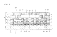
- FIG. 1 is a cross-sectional view showing a structure of a component built-in board mounting body according to a first embodiment of the present invention.
- a component built-in board mounting body 100 according to the first embodiment is configured from a component built-in board 1 and a mounting board 2 on a mounting surface 2a of which the component built-in board 1 is mounted.
- the component built-in board 1 comprises a structure in which a first printed wiring base 10, a second printed wiring base 20, a third printed wiring base 30, and a fourth printed wiring base 40 are stacked collectively by thermal compression bonding. Moreover, the component built-in board 1 comprises an electronic component 90 which is built in to an opening 29 formed in a second resin base 21 of the second printed wiring base 20, in a state of being sandwiched by the first and third printed wiring bases 10 and 30. Furthermore, the component built-in board 1 comprises a bump 49 formed on a mounting surface 2a side of the fourth printed wiring base 40.
- the first through fourth printed wiring bases 10 to 40 respectively comprise: first through fourth resin bases 11, 21, 31, and 41; and signal-dedicated wiring lines 32 and 42, and thermal wiring lines 13, 23, 33, and 43 formed on at least one surface of these first through fourth resin bases.
- the first through fourth printed wiring bases 10 to 40 respectively comprise thermal vias 14, 34, and 44 that are formed by filling inside via holes formed in the first, third, and fourth resin bases 11, 31, and 41, and a thermal via 24 that is formed inside a via hole formed in the second resin base 21 such that both surfaces of the second resin base 21 are electrically continuous, and signal-dedicated vias 35 and 45.
- thermal vias 14, 34, and 44 that are formed by filling inside via holes formed in the first, third, and fourth resin bases 11, 31, and 41
- a thermal via 24 that is formed inside a via hole formed in the second resin base 21 such that both surfaces of the second resin base 21 are electrically continuous, and signal-dedicated vias 35 and 45.
- Employable as these first through fourth printed wiring bases 10 to 40 are, for example, a single-sided copper clad laminated board (single-sided CCL) or a double-sided copper clad laminated board (double-sided CCL), and so on.
- the second printed wiring base 20 is formed based on a double-sided CCL, and the other printed wiring bases are formed based on a single-sided CCL. Therefore, the thermal wiring line 23 of the second printed wiring base 20 is formed on both surfaces of the second resin base 21, and the thermal via 24 provides interlayer connection between the thermal wiring line 23 of both these surfaces.
- the thermal via 24 is configured from a structure in which, for example, a plating is applied inside a through-hole formed from a side of one of the thermal wiring lines 23 without penetrating the other of the thermal wiring lines 23, and is formed by a copper plating. At this time, it is also possible to adopt a structure where the inside of the through-hole is filled with a conductive paste instead of being plated.
- the first through fourth resin bases 11 to 41 are each configured by, for example, a resin film having a thickness of about 25 ⁇ m.
- a resin film configured from the likes of a thermoplastic polyimide, polyolefin, or liquid crystal polymer, or a resin film configured from a thermosetting epoxy resin, and so on.
- the electronic component 90 is the likes of a semiconductor component such as an IC chip, for example, or a passive component, and the electronic component 90 in FIG. 1 indicates a WLP (Wafer Level Package) that has been rewired. Formed on an electrode formation surface 91b of the electronic component 90 are a plurality of rewiring electrodes 91.
- the signal-dedicated wiring lines 32 and 42, and the thermal wiring lines 13 to 43 are configured by pattern-forming a conductive material such as copper foil.
- the signal-dedicated vias 35 and 45, and the thermal vias 14, 34, and 44 are configured from a conductive paste respectively filled into the via holes, and the thermal via 24 is formed by plating.
- the thermal wiring lines and thermal vias, excluding a portion thereof, are formed to be disposed on an outer peripheral side of the electronic component 90.
- the conductive paste includes, for example, at least one kind of metallic particle of low electrical resistance selected from the likes of nickel, gold, silver, zinc, aluminum, iron, and tungsten, and at least one kind of metallic particle of low melting point selected from the likes of bismuth, indium, and lead.
- the conductive paste is configured from a paste that has tin included as a component in these metallic particles, and has mixed into these metallic particles a binder component whose main component is an epoxy, an acrylic, a urethane, and so on.
- the conductive paste configured in this way enables the included tin and the metal of low melting point contained therein to melt and form an alloy at a temperature of 200°C or less, specifically the likes of copper or silver comprise characteristics allowing an intermetallic compound to be formed.
- the conductive paste may also be configured by a nanopaste in which, for example, a filler of the likes of gold, silver, copper, or nickel with a nanolevel particle diameter is mixed into a binder component of the above-described kind.
- the conductive paste may also be configured by a paste having metallic particles of the above-described nickel, and so on, mixed into a binder component of the above-described kind.
- the conductive paste is characterized in that electrical connection is performed by contact between fellow metallic particles.
- Employable as a method of filling the conductive paste into the via holes is, for example, a printing method, a spin coating method, a spray coating method, a dispensing method, a laminating method, a method combining use of these methods, and so on.
- the bump 49 is configured from the likes of solder, and is formed at a portion above the signal-dedicated wiring line 42 and the thermal wiring line 43 formed on the mounting surface 2a side of the fourth resin base 41 of the fourth printed wiring base 40 not covered by a solder resist 48.
- the component built-in board 1 is mounted on the mounting surface 2a of the mounting board 2 via these bumps 49.
- the first through fourth printed wiring bases 10 to 40 are stacked via an adhesive layer 9.
- the adhesive layer 9 is configured from the likes of an epoxy system or acrylic system adhesive agent, or the likes of an organic system adhesive agent including a volatile component.
- the component built-in board mounting body 100 configured in this way leads to a structure in which the electronic component 90 is disposed between the thermal wiring line 13 of the first printed wiring base 10 and the mounting board 2. Heat of the electronic component 90 built in to the component built-in board 1 in this way follows the following heat radiation path to be transmitted to the mounting board 2. That is, heat of the electronic component 90 is transmitted from a back surface 91a on an opposite side to an electrode formation surface 91b of the electronic component 90 to the thermal via 14 of the first printed wiring base 10 connected to this back surface 14.
- Heat transmitted to the thermal via 14 passes from the thermal wiring line 13 of the first printed wiring base 10 through the thermal via 14 formed on the outer peripheral side of the electronic component 90 to be transmitted to the thermal wiring line 23 of the second printed wiring base 20, and is then transmitted to the thermal via 34 of the third printed wiring base 30 via the thermal via 24 and the thermal wiring line 23.
- Heat transmitted to the thermal via 34 passes through the thermal wiring line 33 of the third printed wiring base 30 to be transmitted to the thermal via 44 of the fourth printed wiring base 40 and be transmitted to the bump 49 via the thermal wiring line 43. Heat transmitted to the bump 49 in this way is transmitted via this bump 49 to the mounting board 2 which has an area larger than that of the component built-in board 1, to be radiated from the mounting board 2.
- FIG. 2 is a flowchart showing a manufacturing process of the component built-in board mounting body.
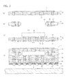
- FIG. 3 is a cross-sectional view showing the component built-in board mounting body on a manufacturing process basis.
- a plurality of resin bases each of which is, for example, a single-sided copper clad laminated board (single-sided CCL), or the like, and that each have a conductor layer formed on one of surfaces thereof, are prepared (step S100), and undergo etching, or the like, to each have a wiring pattern of signal-dedicated wiring lines and thermal wiring lines, and so on, formed therein (step S102).
- an adhesive agent is applied to the resin base to form an adhesive layer (step S104), and a via hole is formed by a laser processing machine (step S106). Then, conductive paste is filled into the via hole to form a signal-dedicated via and a thermal via (step S108).
- a plurality of basic printed wiring bases each having a wiring pattern and vias, of the likes of the first printed wiring base 10 of the kind shown in FIG. 3(a) , the third printed wiring base 30 of the kind shown in FIG. 3 (c) , or the fourth printed wiring base 40, and so on.
- the second resin base 21 which is, for example, a double-sided copper clad laminated board (double-sided CCL), or the like, has a through-hole formed therein, from a side of one of the thermal wiring lines 23 (in particular, a land portion connected to the thermal wiring line 23), so as to not penetrate the other of the thermal wiring lines 23 (in particular, a land portion connected to the thermal wiring line 23), the inside of the through-hole is plated to form the thermal via 24, and then the opening 29 is formed (step S110).
- the first through fourth printed wiring bases 10 to 40 are prepared.
- a rewiring electrode 91 of the electronic component 90 is aligned with the signal-dedicated via 35 of the third printed wiring base 30 by a mounting device for an electronic component, and the electronic component 90 is provisionally adhered by applying heat at a temperature less than or equal to a curing temperature of the adhesive layer 9 of the third printed wiring base 30 and the conductive paste of the signal-dedicated via 35 (step S112).
- the first through fourth printed wiring bases 10 to 40 are each aligned and collectively stacked by, for example, performing thermal compression bonding at a heating temperature of 200°C or less (step S114), thereby producing the component built-in board 1.
- the fourth resin base 41 on a signal-dedicated wiring line 42 and thermal wiring line 43 side of the fourth printed wiring base 40 in the component built-in board 1 has the solder resist 48 pattern-formed thereon (step S116), each of the wiring lines 42 and 43 have the bump 49 formed thereon (step S118), and the component built-in board 1 is mounted on the mounting board 2 (step S120), thereby manufacturing the component built-in board mounting body 100 of the kind shown in FIG. 1 .
- solder resist 48 not illustrated is formed covering the thermal wiring line 13 above the first resin base 11 shown in FIG. 1 .
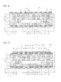
- FIG. 4 is a cross-sectional view showing a structure of a component built-in board mounting body according to a second embodiment of the present invention.
- a component built-in board mounting body 200 according to the second embodiment differs from the component built-in board mounting body 100 according to the first embodiment in having the component built-in board 1 mounted face up (up and down reversed) on the mounting surface 2a of the mounting board 2, and in having a connection mode of the signal-dedicated wiring lines and thermal wiring lines of each of the printed wiring bases 10 to 40 changed due to a pattern of the thermal wiring line 13 of the first printed wiring base 10 being changed.
- solder resist 48 pattern-formed on the first resin base 11 on a thermal wiring line 13 side of the first printed wiring base 10 in the component built-in board 1 is provided, the bump 49 is formed on the signal-dedicated line 12 and the thermal wiring line 13, and the component built-in board 1 is mounted on the mounting board 2 via this bump 49.
- additionally formed in the first and second printed wiring bases 10 and 20 are a signal-dedicated wiring line 22 and signal-dedicated vias 15 and 25.
- the component built-in board mounting body 200 configured in this way has a structure inwhich the thermal wiring line 13 of the first printed wiring base 10 is disposed between the electronic component 90 and the mounting board 2. Therefore, heat of the electronic component 90 built in to the component built-in board 1 is transmitted from the back surface 91a to the thermal via 14 of the first printed wiring base 10, and passes through the thermal wiring line 13 and the bump 49 to be transmitted to the mounting board 2. Due to such a structure, a distance in a mounting direction between the electronic component 90 which is a heat generation source and the mounting board 2 which is a heat radiation body is made closer, hence heat radiation characteristics can be further improved over the component built-in board mounting body 100 according to the first embodiment.
- FIG. 5 is a cross-sectional view showing a structure of a component built-in board mounting body according to a third embodiment of the present invention.
- a component built-in board mounting body 300 according to the third embodiment differs from the component built-in board mounting body 200 according to the second embodiment in having an electronic component 98 (second electronic component) further surface-mounted on the component built-in board mounting body 200 according to the second embodiment having the electronic component 90 (first electronic component) built in thereto.
- a first bump 49 is formed on the signal-dedicated wiring line 12 and the thermal wiring line 13 of the first printed wiring base 10 in the component built-in board 1, and the solder resist 48 pattern-formed on the fourth resin base 41 on a signal-dedicated wiring line 42 side of the fourth printed wiring base 40 is further provided and a second bump 97 is formed on the signal-dedicated wiring line 42.
- an electrode 99 of the electronic component 98 is connected to the signal-dedicated wiring line 42 via the second bump 97, and the electronic component 98 is surface-mounted on the component built-in board 1 via an underfill 96 formed filling in between an electrode formation surface 99b of the electronic component 98 and the solder resist 48.
- the component built-in board 1 is mounted on the mounting surface 2a of the mounting board 2 via the first bump 49.
- a signal transmission path (signal distance) between the rewiring electrode 91 of the electronic component 90 built in to the component built-in board 1 and the electrode 99 of the surface-mounted electronic component 98 can be shortened, whereby signal speed can be improved.
- heat of the electronic components 90 and 98 built in to and surface-mounted on the component built-in board 1 passes through a path of all of the signal-dedicated wiring lines 12, 22, 32, and 42, and the signal-dedicated vias 15, 25, 35, and 45 linked to the first bump, including a path due to the thermal via 14 and the thermal wiring line 13 on the back surface 91a side of the electronic component 90, to be transmitted from the first bump 49 to the mounting board 2.
- a signal distance and a heat radiation path from the electronic components 90 and 98 which are heat generation sources to the mounting board 2 which is a heat radiation body can each be shortened, hence heat radiation characteristics can be further improved while improving signal speed.
- flexibility of wiring design can be improved.
- FIG. 6 is a cross-sectional view showing another structure of the component built-in board mounting body.
- the component built-in board mounting body 300 may be configured such that the component built-in board 1 is mounted on the mounting board 2 in a state where an entirety of a surface mounting side of the electronic component 98 of the fourth printed wiring base 40 of the component built-in board 1 is, for example, covered by a mold resin 95, instead of the underfill 96 provided on a side of the electrode formation surface 99b of the electrode 99 of the electronic component 98.
- FIG. 7 is a view showing an analysis result of heat radiation characteristics of the component built-in board mounting body according to examples of embodiments of the present invention and a component built-in board mounting body of comparative examples.
- the vertical axis of FIG. 7 indicates Tj temperature.
- Both the examples of embodiments and the comparative examples employed a component built-in board mounting body in which the component built-in board of four-layer structure of the above-described kind is mounted on the mounting board.
- Comparative example 1 is a component built-in board mounting body having mounted on the mounting board thereof a component built- in board of a structure in which the electrode of the electronic component is disposed on a mounting board side, without the thermal via being formed on a back surface side of the electronic component.
- comparative example 2 is a component built-in board mounting body having mounted on the mounting board thereof a component built- in board of a structure in which the thermal via is formed on a back surface side of the electronic component, a heat radiation board connected to this thermal via is formed on a surface layer, and the electrode of the electronic component is disposed on a mounting board side.
- Example 1 and example 2 are respectively configured by structures similar to those of the component built-in board mounting bodies 100 and 200.
- Tj temperature employed general-purpose software "ANSYS (Registered Trademark)", with the following boundary conditions of analysis. That is, for comparative examples 1 and 2, and examples 1 and 2, analysis was performed by applying a calorific value of 1 watt (W) to the electronic component built in to the component built-in board, assuming a static state of no convection current of external air on an external air contact surface of the component built-in board mounting body, in an environment of ambient air temperature 25°C with a heat transmission coefficient of 4.5 W/m 2 k.
- W 1 watt
- Tj temperature in both comparative examples 1 and 2 attained in the neighborhood of 115°C
- Tj temperature in example 1 attained in the neighborhood of 97.5°C
- example 2 attained about 94°C.
Landscapes
- Engineering & Computer Science (AREA)
- Microelectronics & Electronic Packaging (AREA)
- Manufacturing & Machinery (AREA)
- Production Of Multi-Layered Print Wiring Board (AREA)
- Structure Of Printed Boards (AREA)
- Cooling Or The Like Of Semiconductors Or Solid State Devices (AREA)
Applications Claiming Priority (2)
| Application Number | Priority Date | Filing Date | Title |
|---|---|---|---|
| JP2011216527A JP5100878B1 (ja) | 2011-09-30 | 2011-09-30 | 部品内蔵基板実装体及びその製造方法並びに部品内蔵基板 |
| PCT/JP2012/074562 WO2013047520A1 (fr) | 2011-09-30 | 2012-09-25 | Corps de montage de substrat à composant intégré, son procédé de fabrication et substrat à composant intégré |
Publications (2)
| Publication Number | Publication Date |
|---|---|
| EP2763518A1 true EP2763518A1 (fr) | 2014-08-06 |
| EP2763518A4 EP2763518A4 (fr) | 2015-07-22 |
Family
ID=47528470
Family Applications (1)
| Application Number | Title | Priority Date | Filing Date |
|---|---|---|---|
| EP12835560.9A Withdrawn EP2763518A4 (fr) | 2011-09-30 | 2012-09-25 | Corps de montage de substrat à composant intégré, son procédé de fabrication et substrat à composant intégré |
Country Status (4)
| Country | Link |
|---|---|
| US (1) | US9635763B2 (fr) |
| EP (1) | EP2763518A4 (fr) |
| JP (1) | JP5100878B1 (fr) |
| WO (1) | WO2013047520A1 (fr) |
Cited By (1)
| Publication number | Priority date | Publication date | Assignee | Title |
|---|---|---|---|---|
| US11355465B2 (en) | 2017-10-11 | 2022-06-07 | Sony Semiconductor Solutions Corporation | Semiconductor device including glass substrate having improved reliability and method of manufacturing the same |
Families Citing this family (15)
| Publication number | Priority date | Publication date | Assignee | Title |
|---|---|---|---|---|
| US9711428B2 (en) * | 2013-09-27 | 2017-07-18 | Intel Corporation | Dual-sided die packages |
| US9826646B2 (en) * | 2014-05-27 | 2017-11-21 | Fujikura Ltd. | Component built-in board and method of manufacturing the same, and mounting body |
| JP5913535B1 (ja) * | 2014-11-19 | 2016-04-27 | 株式会社フジクラ | 部品内蔵基板及びその製造方法 |
| DE102015104641B4 (de) * | 2015-03-26 | 2025-03-13 | At & S Austria Technologie & Systemtechnik Ag | Träger mit passiver Kühlfunktion für ein Halbleiterbauelement |
| CN107615894B (zh) * | 2015-06-03 | 2020-07-17 | 株式会社村田制作所 | 元器件安装基板 |
| WO2017039275A1 (fr) | 2015-08-31 | 2017-03-09 | 한양대학교 산학협력단 | Structure de boîtier de semi-conducteur et son procédé de fabrication |
| KR101923659B1 (ko) * | 2015-08-31 | 2019-02-22 | 삼성전자주식회사 | 반도체 패키지 구조체, 및 그 제조 방법 |
| US20200161206A1 (en) * | 2018-11-20 | 2020-05-21 | Advanced Semiconductor Engineering, Inc. | Semiconductor package structure and semiconductor manufacturing process |
| CN111463190B (zh) * | 2020-04-10 | 2022-02-25 | 青岛歌尔智能传感器有限公司 | 传感器及其制作方法、以及电子设备 |
| US12610451B2 (en) | 2020-04-27 | 2026-04-21 | At&S Austria Technologie & Systemtechnik Aktiengesellschaft | Component carrier with an embedded thermally conductive block and manufacturing method |
| DE102021109974A1 (de) | 2020-04-27 | 2021-10-28 | At & S Austria Technologie & Systemtechnik Aktiengesellschaft | Bauteilträger mit einem eingebetteten wärmeleitfähigen Block und Herstellungsverfahren |
| TW202214065A (zh) * | 2020-08-07 | 2022-04-01 | 日商昭和電工材料股份有限公司 | 零件內建基板之製造方法及零件內建基板 |
| JP7744154B2 (ja) * | 2021-03-30 | 2025-09-25 | 株式会社デンソー | 回路基板内に電気部品を備える半導体装置 |
| EP4095898A1 (fr) * | 2021-05-25 | 2022-11-30 | Mitsubishi Electric R&D Centre Europe B.V. | Carte de circuits imprimés améliorée thermiquement pour puce de puissance connectée par technique via et ensemble utilisant une telle carte de circuits imprimés |
| CN121694066A (zh) * | 2023-07-26 | 2026-03-17 | 长江存储科技有限责任公司 | 芯片封装结构、半导体结构及其制作方法 |
Family Cites Families (22)
| Publication number | Priority date | Publication date | Assignee | Title |
|---|---|---|---|---|
| JPH07226456A (ja) * | 1993-04-23 | 1995-08-22 | Nippon Micron Kk | Icパッケージ及びその製造方法 |
| JP2002198660A (ja) * | 2000-12-27 | 2002-07-12 | Kyocera Corp | 回路基板及びその製造方法 |
| JP2002299775A (ja) * | 2001-03-30 | 2002-10-11 | Kyocera Corp | 電子部品装置 |
| US20020175402A1 (en) * | 2001-05-23 | 2002-11-28 | Mccormack Mark Thomas | Structure and method of embedding components in multi-layer substrates |
| TW550997B (en) * | 2001-10-18 | 2003-09-01 | Matsushita Electric Industrial Co Ltd | Module with built-in components and the manufacturing method thereof |
| JP3937840B2 (ja) * | 2002-01-10 | 2007-06-27 | 株式会社日立製作所 | 高周波モジュール |
| JP2006019441A (ja) * | 2004-06-30 | 2006-01-19 | Shinko Electric Ind Co Ltd | 電子部品内蔵基板の製造方法 |
| JP2006019361A (ja) * | 2004-06-30 | 2006-01-19 | Sanyo Electric Co Ltd | 回路装置およびその製造方法 |
| JP4535801B2 (ja) * | 2004-07-28 | 2010-09-01 | 京セラ株式会社 | セラミック配線基板 |
| JP2006108483A (ja) * | 2004-10-07 | 2006-04-20 | Hitachi Metals Ltd | キャビティを備えた多層セラミック基板およびその製造方法 |
| JP4718889B2 (ja) * | 2005-04-28 | 2011-07-06 | 日本特殊陶業株式会社 | 多層配線基板及びその製造方法、多層配線基板構造体及びその製造方法 |
| DE102005037040A1 (de) * | 2005-08-05 | 2007-02-08 | Epcos Ag | Elektrisches Bauelement |
| US8101868B2 (en) * | 2005-10-14 | 2012-01-24 | Ibiden Co., Ltd. | Multilayered printed circuit board and method for manufacturing the same |
| JP2008098285A (ja) * | 2006-10-10 | 2008-04-24 | Rohm Co Ltd | 半導体装置 |
| JP5326269B2 (ja) * | 2006-12-18 | 2013-10-30 | 大日本印刷株式会社 | 電子部品内蔵配線板、及び電子部品内蔵配線板の放熱方法 |
| JP5075424B2 (ja) | 2007-02-19 | 2012-11-21 | 株式会社フジクラ | 電子部品内蔵型配線基板の製造方法 |
| JP4833192B2 (ja) * | 2007-12-27 | 2011-12-07 | 新光電気工業株式会社 | 電子装置 |
| JP5221228B2 (ja) * | 2008-07-10 | 2013-06-26 | 日本特殊陶業株式会社 | 部品内蔵配線基板及びその製造方法 |
| JP5442236B2 (ja) * | 2008-11-14 | 2014-03-12 | 新光電気工業株式会社 | 電子部品内蔵配線基板の製造方法、電子部品内蔵配線基板及び半導体装置 |
| JP2010123632A (ja) * | 2008-11-17 | 2010-06-03 | Shinko Electric Ind Co Ltd | 電子部品内蔵配線基板の製造方法 |
| JP4973761B2 (ja) * | 2009-05-25 | 2012-07-11 | 株式会社デンソー | 半導体装置 |
| JP5494586B2 (ja) * | 2010-09-30 | 2014-05-14 | 大日本印刷株式会社 | 電圧変換モジュール |
-
2011
- 2011-09-30 JP JP2011216527A patent/JP5100878B1/ja active Active
-
2012
- 2012-09-25 EP EP12835560.9A patent/EP2763518A4/fr not_active Withdrawn
- 2012-09-25 WO PCT/JP2012/074562 patent/WO2013047520A1/fr not_active Ceased
-
2014
- 2014-03-28 US US14/229,425 patent/US9635763B2/en active Active
Cited By (1)
| Publication number | Priority date | Publication date | Assignee | Title |
|---|---|---|---|---|
| US11355465B2 (en) | 2017-10-11 | 2022-06-07 | Sony Semiconductor Solutions Corporation | Semiconductor device including glass substrate having improved reliability and method of manufacturing the same |
Also Published As
| Publication number | Publication date |
|---|---|
| EP2763518A4 (fr) | 2015-07-22 |
| US20140211437A1 (en) | 2014-07-31 |
| US9635763B2 (en) | 2017-04-25 |
| JP2013077691A (ja) | 2013-04-25 |
| WO2013047520A1 (fr) | 2013-04-04 |
| JP5100878B1 (ja) | 2012-12-19 |
Similar Documents
| Publication | Publication Date | Title |
|---|---|---|
| US9635763B2 (en) | Component built-in board mounting body and method of manufacturing the same, and component built-in board | |
| US10128214B2 (en) | Substrate and the method to fabricate thereof | |
| US6373131B1 (en) | TBGA semiconductor package | |
| US9179549B2 (en) | Packaging substrate having embedded passive component and fabrication method thereof | |
| US20100193937A1 (en) | Semiconductor module | |
| US9560770B2 (en) | Component built-in board and method of manufacturing the same, and mounting body | |
| US9269685B2 (en) | Integrated circuit package and packaging methods | |
| TW201804579A (zh) | 功率覆蓋結構及其製造方法 | |
| EP2787799A1 (fr) | Carte à composant incorporé et son procédé de fabrication, et conditionnement avec carte à composant incorporé | |
| US8058723B2 (en) | Package structure in which coreless substrate has direct electrical connections to semiconductor chip and manufacturing method thereof | |
| US11450597B2 (en) | Semiconductor package substrate having heat dissipating metal sheet on solder pads, method for fabricating the same, and electronic package having the same | |
| KR100661946B1 (ko) | 회로 장치 및 그 제조 방법 | |
| US11289412B2 (en) | Package substrate with partially recessed capacitor | |
| KR20190004964A (ko) | 반도체 패키지 | |
| US9425116B2 (en) | Integrated circuit package and a method for manufacturing an integrated circuit package | |
| US9105562B2 (en) | Integrated circuit package and packaging methods | |
| US20110147058A1 (en) | Electronic device and method of manufacturing electronic device | |
| JPH09199823A (ja) | チップオンボードプリント配線板 | |
| CN108807331A (zh) | 电子封装件及其制法 | |
| CN101331605A (zh) | 电子部件内置模块和其制造方法 | |
| US20060108146A1 (en) | Structure of electronic package and method for fabricating the same | |
| CN217983329U (zh) | 半导体封装结构 | |
| CN106158787B (zh) | 封装装置与其制作方法 | |
| JP2014067819A (ja) | 部品内蔵基板実装体及びその製造方法並びに部品内蔵基板 | |
| JP6985599B2 (ja) | 電子装置及び電子装置の製造方法 |
Legal Events
| Date | Code | Title | Description |
|---|---|---|---|
| PUAI | Public reference made under article 153(3) epc to a published international application that has entered the european phase |
Free format text: ORIGINAL CODE: 0009012 |
|
| 17P | Request for examination filed |
Effective date: 20140327 |
|
| AK | Designated contracting states |
Kind code of ref document: A1 Designated state(s): AL AT BE BG CH CY CZ DE DK EE ES FI FR GB GR HR HU IE IS IT LI LT LU LV MC MK MT NL NO PL PT RO RS SE SI SK SM TR |
|
| DAX | Request for extension of the european patent (deleted) | ||
| RA4 | Supplementary search report drawn up and despatched (corrected) |
Effective date: 20150618 |
|
| RIC1 | Information provided on ipc code assigned before grant |
Ipc: H05K 1/02 20060101ALI20150612BHEP Ipc: H05K 3/46 20060101AFI20150612BHEP Ipc: H01L 23/498 20060101ALI20150612BHEP Ipc: H01L 23/367 20060101ALI20150612BHEP Ipc: H01L 23/31 20060101ALI20150612BHEP Ipc: H01L 23/538 20060101ALI20150612BHEP Ipc: H01L 23/36 20060101ALI20150612BHEP Ipc: H01L 23/12 20060101ALI20150612BHEP |
|
| STAA | Information on the status of an ep patent application or granted ep patent |
Free format text: STATUS: THE APPLICATION HAS BEEN WITHDRAWN |
|
| 18W | Application withdrawn |
Effective date: 20190927 |